Table of Contents
Advertisement
Quick Links
SERVICE MANUAL
Main Section
I Specifications
I Preparation for Servicing
I Adjustment Procedures
I Schematic Diagrams
I CBA's
I Exploded Views
I Parts List
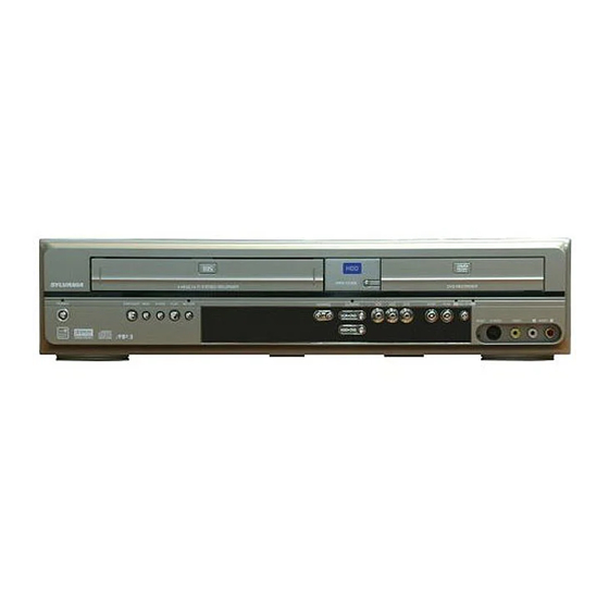
DVD/Video Cassette Recorder
POWER
with HDD
HDRV200F
STOP/EJECT REW
F.FWD
PLAY
REC/OTR
The Part No. of the Deck
Mechanism used in this model is
N2461FL, but when servicing the
deck mechanism, refer to
N2460FL in the MK14 Deck
Mechanism Section.
OPEN / CLOSE
CHANNEL
DUBBING
VCR
HDD
DVD
STOP
PLAY
HDD
REC/OTR
VCR DVD
HDD DVD
DVD
S-VIDEO
VIDEO
L
AUDIO
R
Advertisement
Table of Contents

Related Manuals for Sylvania HDRV200F


Summary of Contents for Sylvania HDRV200F
- Page 1 I Schematic Diagrams deck mechanism, refer to I CBA’s N2460FL in the MK14 Deck I Exploded Views Mechanism Section. I Parts List DVD/Video Cassette Recorder with HDD HDRV200F OPEN / CLOSE POWER STOP/EJECT REW F.FWD PLAY REC/OTR CHANNEL DUBBING STOP...
- Page 2 IMPORTANT SAFETY NOTICE Proper service and repair is important to the safe, reliable operation of all Funai Equipment. The service procedures recommended by Funai and described in this service manual are effective methods of performing service operations. Some of these service special tools should be used when and as recommended.
-
Page 3: Table Of Contents
MAIN SECTION DVD/Video Cassette Recorder with HDD HDRV200F Main Section I Specifications I Preparation for Servicing I Adjustment Procedures I Schematic Diagrams I CBA’s I Exploded Views I Parts List TABLE OF CONTENTS Specifications ................1-1-1 Laser Beam Safety Precautions . -
Page 4: Specifications
SPECIFICATIONS ITEM General Internal 3.5 inch HDD 160 GB Power consumption 44W (standby: 4.6W) Recording Recording format Video Recording Format (DVD-RW only) Video Format (DVD-RW, DVD-R) Recordable discs DVD-ReWritable DVD-Recordable Video recording format Sampling frequency 13.5MHz Compression format MPEG Audio recording format Sampling frequency 48kHz Compression format... -
Page 5: Laser Beam Safety Precautions
LASER BEAM SAFETY PRECAUTIONS This DVD player uses a pickup that emits a laser beam. Do not look directly at the laser beam coming from the pickup or allow it to strike against your skin. The laser beam is emitted from the location shown in the figure. When checking the laser diode, be sure to keep your eyes at least 30 cm away from the pickup lens when the diode is turned on. -
Page 6: Important Safety Precautions
IMPORTANT SAFETY PRECAUTIONS Product Safety Notice Also check areas surrounding repaired locations. J. Be careful that foreign objects (screws, solder Some electrical and mechanical parts have special droplets, etc.) do not remain inside the set. safety-related characteristics which are often not K. - Page 7 Safety Check after Servicing Examine the area surrounding the repaired location for damage or deterioration. Observe that screws, parts, and wires have been returned to their original positions. Afterwards, do the following tests and confirm the specified values to verify compliance with safety standards. 1.
-
Page 8: Standard Notes For Servicing
STANDARD NOTES FOR SERVICING Circuit Board Indications Pb (Lead) Free Solder 1. The output pin of the 3 pin Regulator ICs is When soldering, be sure to use the Pb free solder. indicated as shown. How to Remove / Install Flat Pack-IC Top View Bottom View 1. - Page 9 3. The flat pack-IC on the CBA is affixed with glue, so With Soldering Iron: be careful not to break or damage the foil of each 1. Using desoldering braid, remove the solder from pin or the solder lands under the IC when all pins of the flat pack-IC.
- Page 10 2. Installation With Iron Wire: 1. Using desoldering braid, remove the solder from 1. Using desoldering braid, remove the solder from all pins of the flat pack-IC. When you use solder the foil of each pin of the flat pack-IC on the CBA flux which is applied to all pins of the flat pack-IC, so you can install a replacement flat pack-IC more you can remove it easily.
- Page 11 Instructions for Handling Semi- conductors Electrostatic breakdown of the semi-conductors may occur due to a potential difference caused by electrostatic charge during unpacking or repair work. 1. Ground for Human Body Be sure to wear a grounding band (1 MΩ) that is properly grounded to remove any static electricity that may be charged on the body.
-
Page 12: Handling Precautions For Hdd
HANDLING PRECAUTIONS FOR HDD CAUTION: 4. OTHERS a. Be careful so as not to do the followings. 1. SHOCK Otherwise, HDD might be damaged. a. Exposing HDD to shock may be the biggest - DO NOT disassemble HDD. damaging factor. Please note that HDD is easily - When handling HDD, be sure to hold both sides damaged even if dropped from any height. -
Page 13: Preparation For Servicing
PREPARATION FOR SERVICING How to Enter the Service Mode About Optical Sensors Caution: An optical sensor system is used for the Tape Start and End Sensors on this equipment. Carefully read and follow the instructions below. Otherwise the unit may operate erratically. What to do for preparation Insert a tape into the Deck Mechanism Assembly and press [VCR PLAY] button. -
Page 14: Cabinet Disassembly Instructions
CABINET DISASSEMBLY INSTRUCTIONS 1. Disassembly Flowchart REMOVAL This flowchart indicates the disassembly steps to gain REMOVE/*UNHOOK/ LOC. PART Fig. access to item(s) to be serviced. When reassembling, UNLOCK/RELEASE/ Note follow the steps in reverse order. Bend, route, and UNPLUG/DESOLDER dress the cables as they were originally. Mechanism [1] Top Cover 2(S-5), 2(S-6),... - Page 15 (4): Identification of parts to be removed, unhooked, unlocked, released, unplugged, unclamped, or desoldered. (S-1) [1] Top Cover P=Spring, L=Locking Tab, S=Screw, CN=Connector (S-1) *=Unhook, Unlock, Release, Unplug, or Desolder (S-1) e.g. 6(S-1) = six Screws (S-1), 5(L-1) = five Locking Tabs (L-1) (5): Refer to “Reference Notes.”...
- Page 16 [5] DVD Mechanism & (S-10) (S-11) DVD/HDD Main CBA (S-9) (S-10) [4] HDD Assembly Assembly (S-11) Wire (S-4) (S-6) Sheet (S-4) (S-5) [11] Fan Motor (S-6) CN4001 [10] Fan Holder [12] Rear Panel CN201 CN2203 CN2204 Fig. D5 [14] Open/Close CBA CN2201 Desolder [15] Front Jack CBA...
- Page 17 Cylinder Assembly FE Head ACE Head Assembly SW4512 LD-SW [17] Deck Assembly [19] Power [18] AV CBA SW CBA [17] Deck Assembly Cam Gear Hole (S-18) Shaft [18] AV CBA Desolder (S-19) Hole LD-SW [18] AV CBA Lead with blue stripe From FE Head From...
- Page 18 (S-20) [20] Deck Pedestal (S-20) [21] Front Bracket R [22] Bracket R (S-22) (S-21) Fig. D9 3. How to Eject Manually < Method 1 > Note: When servicing, do not touch white resin part as shown below. When rotating the gear, be careful not to damage the gear. 1.
- Page 19 < Method 2 > Note: When servicing, do not touch white resin part 4. Release the other side of two Locking Tabs, and as shown below. remove the Clamper Assembly. 1. Remove the Top Cover, the Front Assembly and the DVD Mechanism & DVD/HDD Main CBA Clamper Assembly Assembly.
-
Page 20: Electrical Adjustment Instructions
ELECTRICAL ADJUSTMENT INSTRUCTIONS General Note: “CBA” is abbreviation for Head Switching Position “Circuit Board Assembly.” Adjustment NOTE: Purpose: To determine the Head Switching position 1. Electrical adjustments are required after replacing during playback. circuit components and certain mechanical parts. Symptom of Misadjustment: May cause Head It is important to do these adjustments only after Switching noise or vertical jitter in the picture. -
Page 21: How To Self-Check And Initialize The Dvd/Vcr With Hdd
HOW TO SELF-CHECK AND INITIALIZE THE DVD/VCR WITH HDD 1. Turn on the DVD/VCR with HDD recorder. 2. To put the DVD/VCR with HDD recorder into the HDD mode, press [HDD] on the remote control unit. 3. To put the DVD/VCR with HDD recorder into the self-check mode, after pressing [VARIABLE SKIP] button, press the [3], [6], and [9] buttons on the remote control in that order within three seconds. - Page 22 Table 2: Indication of DVD self-check (*7) INDICATION DESCRIPTION Connection of DVD is normal. NOT FOUND DVD drive cannot be found. FFC cable (connecting to CN401) between the DVD drive and the DVD/HDD Main CBA is CABLE ERROR not connected correctly. Table 3: Indication of HDD self-check (*8) INDICATION DESCRIPTION...
-
Page 23: Firmware Renewal Mode
FIRMWARE RENEWAL MODE 1. Update Contents 4. Load the update disc. The TV screen will display Fig. c. Item Status - If the update disc contains only a single file, the update will initiate automatically when the disc is Update B/E FIRMWARE inserted. - Page 24 3. How to Verify the Firmware The status displayed in *2 is as shown below. Version Display Status 1. Turn the power on and remove the disc in the tray. Loading F/W from Update Disc or EXECUTING writing to Flash memory 2.
-
Page 25: Function Indicator Symbols
FUNCTION INDICATOR SYMBOLS < VCR Section > Note: If a mechanical malfunction occurs, the power is turned off. The following symbols will appear on the display. Status Display When reel or capstan mechanism is not functioning correctly When tape loading mechanism is not functioning correctly “W”... - Page 26 < DVD/HDD Section > Note: If an error occurs, a message with the error number appears on the screen. Error message Recording Error Error No. 02-50 Message Error No. Error Description Error Example Renewal error at This code is output when there is a control information writing failure 04-50 ejecting disc due to tray being open during writing or disc loading.
-
Page 27: Block Diagrams
BLOCK DIAGRAMS Servo/System Control Block Diagram 1-12-1 E4380BLS... - Page 28 Sub System Control Block Diagram 1-12-2 E4380BLSS...
- Page 29 Digital Signal Process Block Diagram 1-12-3 E4380BLD...
- Page 30 Video Block Diagram 1-12-4 E4380BLV...
- Page 31 Video Input Select Block Diagram 1-12-5 E4380BLVIS...
- Page 32 Video Output Select Block Diagram 1-12-6 E4380BLVOS...
- Page 33 Audio Block Diagram 1-12-7 E4380BLA...
- Page 34 Audio Input/Output Select Block Diagram 1-12-8 E4380BLAS...
- Page 35 Hi-Fi Audio Block Diagram 1-12-9 E4380BLH...
- Page 36 Power Supply Block Diagram 1-12-10 E4380BLP...
-
Page 37: Schematic Diagrams / Cba's And Test Points
SCHEMATIC DIAGRAMS / CBA’S AND TEST POINTS Standard Notes WARNING Many electrical and mechanical parts in this chassis have special characteristics. These characteristics often pass unnoticed and the protection afforded by them cannot necessarily be obtained by using replacement components rated for higher voltage, wattage, etc. - Page 38 LIST OF CAUTION, NOTES, AND SYMBOLS USED IN THE SCHEMATIC DIAGRAMS ON THE FOLLOWING PAGES: 1. CAUTION: FOR CONTINUED PROTECTION AGAINST FIRE HAZARD, REPLACE ONLY WITH THE SAME TYPE FUSE. ATTENTION: POUR UNE PROTECTION CONTINUE LES RISQES D'INCELE N'UTILISER QUE DES FUSIBLE DE MÊME TYPE. RISK OF FIRE-REPLACE FUSE AS MARKED.
- Page 39 AV 1/8 Schematic Diagram < VCR Section > AV 1/8 Ref No. Position IC4501 TRANSISTORS Q4501 Q4502 Q4506 Q4508 Q4509 Q4510 CONNECTORS CN4501 CN4502 CN4504 VARIABLE RESISTOR VR4501 TEST POINTS TP4508 TP4513 1-13-3 E4380SCAV1...
- Page 40 AV 2/8 & Sensor Schematic Diagram < VCR Section > FL4502 MATRIX CHART TIME P-SCAN SHIFT AV 2/8 TIME P-SCAN Ref No. Position SHIFT IC4571 TRANSISTOR CD R Q4561 TEST POINTS TP4502 TP4506 TP4507 E4380SCAV2 1-13-4...
- Page 41 AV 3/8 Schematic Diagram < VCR Section > AV 3/8 Ref No. Position IC4301 TRANSISTORS Q4301 Q4302 Q4303 Q4421 Q4422 Q4425 Q4426 CONNECTOR CN4253 TEST POINTS TP4301 TP4302 1-13-5 E4380SCAV3...
- Page 42 AV 4/8 Schematic Diagram < VCR Section > AV 4/8 Ref No. Position IC4451 TEST POINT TP4452 1-13-6 E4380SCAV4...
- Page 43 AV 5/8 Schematic Diagram < VCR Section > AV 5/8 Ref No. Position IC4003 IC4005 IC4006 AA-2 IC4007 BB-2 TRANSISTORS Q4004 AA-2 Q4005 AA-1 Q4006 BB-1 Q4025 AA-1 CONNECTORS CN4001 CC-3 CN4002 1-13-7 E4380SCAV5...
- Page 44 AV 6/8 Schematic Diagram < VCR Section > AV 6/8 Ref No. Position IC4008 EE-2 IC4009 FF-4 IC4010 FF-4 IC4011 EE-1 TRANSISTORS Q4013 GG-2 Q4020 FF-1 Q4021 FF-1 Q4022 FF-1 Q4023 GG-1 TEST POINTS JP4015 HH-4 JP4016 HH-4 JP4017 HH-4 1-13-8 E4380SCAV6...
- Page 45 AV 7/8 & Power SW Schematic Diagram < VCR Section > *1 NOTE These components (IC4002, C4174) can be used in any models. However, you cannot mix components under Group A with the ones under Group B. You can choose either Group. The difference between Group A and Group B is shown below.
- Page 46 AV 8/8 Schematic Diagram < VCR Section > AV 8/8 Ref No. Position IC4251 QQ-3 TRANSISTORS Q4251 QQ-3 Q4252 RR-3 Q4256 SS-4 Q4257 RR-2 Q4258 SS-2 Q4264 TT-3 CONNECTOR CN4251 PP-3 1-13-10 E4380SCAV8...
- Page 47 Power Supply Schematic Diagram < VCR Section > CAUTION ! CAUTION ! NOTE: For continued protection against fire hazard, Fixed voltage (or Auto voltage selectable) power supply circuit is used in this unit. The voltage for parts in hot circuit is measured using replace only with the same type fuse.
- Page 48 Front Jack & Open/Close Schematic Diagram < VCR Section > ATA Schematic Diagram < DVD/HDD Section > FRONT JACK Ref No. Position TRANSISTORS Q2501 Q2502 Q2503 Q2504 Q2505 Q2506 CONNECTORS CN2501 CN2502 E4380SCJ E4380SCAT 1-13-12...
- Page 49 DVD/HDD Main 1/6 Schematic Diagram < DVD/HDD Section > DVD/HDD MAIN 1/6 Ref No. Position IC101 IC102 TRANSISTORS Q402 Q403 CONNECTOR CN101 E4380SCM1 1-13-13...
- Page 50 DVD/HDD Main 2/6 Schematic Diagram < DVD/HDD Section > DVD/HDD MAIN 2/6 Ref No. Position IC201 CONNECTOR CN201 1-13-14 E4380SCM2...
- Page 51 DVD/HDD Main 3/6 Schematic Diagram < DVD/HDD Section > DVD/HDD MAIN 3/6 Ref No. Position IC202 IC204 IC401 IC402 IC410 CONNECTORS CN202 CN401 1-13-15 E4380SCM3...
- Page 52 DVD/HDD Main 4/6 Schematic Diagram < DVD/HDD Section > NOTE: 1. The order of pins shown in this diagram is different from that of actual IC601. 2. IC601 is divided into six and shown as IC601 (1/6) ~ IC601 (6/6) in this DVD/HDD Main Schematic Diagram Section. DVD/HDD MAIN 4/6 Ref No.
- Page 53 DVD/HDD Main 5/6 Schematic Diagram < DVD/HDD Section > NOTE: 1. The order of pins shown in this diagram is different from that of actual IC601. 2. IC601 is divided into six and shown as IC601 (1/6) ~ IC601 (6/6) in this DVD/HDD Main Schematic Diagram Section. DVD/HDD MAIN 5/6 Ref No.
- Page 54 DVD/HDD Main 6/6 Schematic Diagram < DVD/HDD Section > NOTE: 1. The order of pins shown in this diagram is different from that of actual IC601. 2. IC601 is divided into six and shown as IC601 (1/6) ~ IC601 (6/6) in this DVD/HDD Main Schematic Diagram Section. DVD/HDD MAIN 6/6 Ref No.
- Page 55 AV CBA Top View Sensor CBA Top View TO SENSOR CBA (END-SENSOR) TP4301 TP4302 TP4513 C-PB RF-SW BHB300F01012A BHB300F01012B JP4017 V-OUT AV CBA Ref No. Position Ref No. Position TRANSISTORS IC4001 Q4303 IC4002 Q4421 IC4003 Q4422 IC4005 Q4425 IC4006 Q4426 IC4007 Q4501 IC4008...
- Page 56 AV CBA Bottom View WF13 PIN 17 OF TU4001 PIN 2 OF IC4008 PIN 3 OF CN4001 PIN 5 OF CN4001 PIN 7 OF CN4001 PIN 9 OF CN4001 PIN 17 OF CN4001 WF10 PIN 1 OF CN4251 1-13-20 BE4340F01045A...
- Page 57 Power Supply CBA Top View CAUTION ! Because a hot chassis ground is present in the power CAUTION ! supply circut, an isolation transformer must be used. For continued protection against fire hazard, Fixed voltage (or Auto voltage selectable) power supply circuit is used in this unit. Also, in order to have the ability to increase the input replace only with the same type fuse.
- Page 58 Power Supply CBA Bottom View CAUTION ! CAUTION ! For continued protection against fire hazard, Because a hot chassis ground is present in the power Fixed voltage (or Auto voltage selectable) power supply circuit is used in this unit. replace only with the same type fuse. supply circut, an isolation transformer must be used.
- Page 59 Power SW CBA Top View Power SW CBA Bottom View Open/Close CBA Top View Open/Close CBA Bottom View BE4340F01045B ATA CBA Top View ATA CBA Bottom View BE4340F01025C BE4340F01032 1-13-23...
- Page 60 Front Jack CBA Top View FRONT JACK Ref No. Position TRANSISTORS Q2501 Q2502 Q2503 Q2504 Q2505 Q2506 CONNECTORS CN2501 CN2502 Front Jack CBA Bottom View BE4340F01025B 1-13-24...
-
Page 61: Waveforms
WAVEFORMS NOTE: Input: COLOR BAR SIGNAL (WITH 1KHz AUDIO SIGNAL) JP4017 Pin 9 of CN4001 Pin 17 of CN4001 V-OUT E-E 0.2V 20µs VIDEO-C 0.2V 20µs AUDIO(L)-OUT 0.5ms JP4017 UPPER Pin 1 of CN4251 Pin 2 of IC4008 TP4302 WF10 LOWER V-OUT 0.5V... - Page 62 WIRING DIAGRAMS Wiring 1/2 Diagram 1-15-1 E4380WI1...
-
Page 63: Wiring Diagram
Wiring 2/2 Diagram 1-15-2 E4380WI2... -
Page 64: System Control Timing Charts
SYSTEM CONTROL TIMING CHARTS < VCR Section > Mode SW: LD-SW LD-SW Position detection A/D Input voltage Limit Symbol (Calculated voltage) 3.76 V ~ 4.50 V (4.12 V) 4.51 V ~ 5.00 V (5.00 V) 0.00 V ~ 0.25 V (0.00 V) 1.06 V ~ 1.50 V (1.21 V) 0.66 V ~ 1.05 V (0.91 V) 1.99 V ~ 2.60 V (2.17 V) - Page 65 Still/Slow Control Frame Advance Timing Chart 1) SP Mode 18 RF-SW The first rise of RF-SW after a rise in F-AD signal F-AD (Internal Signal) "H" "H" "Z" C-DRIVE "L" "L" Stop detection (T2) Acceleration Detection (T1) Slow Tracking Value PB CTL Reversal Limit Value 20ms...
- Page 66 2) LP/SLP Mode 18 RF-SW The first rise of RF-SW after a rise in F-AD signal F-AD (Internal Signal) "H" "H" "Z" C-DRIVE "L" "L" Stop detection (T2) Acceleration Detection (T1) Slow Tracking Value PB CTL Reversal Limit Value 20ms 27 C-F/R 79 H-A-SW 78 C-ROTA...
- Page 67 EJECT ST-S/ END-S "OFF" CASS.LOAD LD-FWD 0.2S LD-REV 0.7S LD-FWD 0.4S LD-FWD 0.2S LD-REV 0.2S LD-FWD 0.5S LD-REV STOP(A) PLAY LD-FWD PLAY LD-FWD LD-REV 0.2S LD-FWD PLAY PLAY PAUSE (SLOW) LD-FWD STILL(SLOW) PLAY LD-REV 0.2S LD-FWD PLAY STOP /EJECT LD-REV STOP(A) Fig.
- Page 68 STOP(A) STOP LD-REV 0.2S LD-FWD STOP /EJECT 1.0S LD-FWD 0.5S LD-REV STOP(A) LD-REV 0.2S LD-FWD STOP /EJECT LD-REV 1.0S LD-FWD 0.5S LD-REV STOP(A) LD-FWD PAUSE LD-FWD 2.5S Short REV LD-REV 0.2S LD-FWD REC PAUSE REC or PAUSE STOP /EJECT LD-FWD 1.5S LD-REV 0.2S...
- Page 69 < DVD/HDD Section > [ Tray Open ] Power on Push Close button is pressed. Tray insertion Case 3 INNER-SW open? [ open ] button is pressed. Is Timer Is slit S5 Case 1 ET3 passed? passed? Rezero 1 Rezero 2 Is Timer Case 4 [ open ] button is pressed.
- Page 70 Parameter S*: Encoder pulse ET*: Error V*: Voltage (HEX) T*: Event timer (HEX) detection timer V0: 2.0 V (00d) S1: 300 (12c) T1: 0.1 s ET1: 5.0 s V1: 4.5 V (022) S2: 3300 (ce4) T2: 3.0 s ET2: 5.0 s V2: 2.2 V (010) S3: 3935 (f5f) T3: 3.0 s...
- Page 71 Tray close Tray ejection direction SLED Tray insersion direction open INNER-SW close Timer Push close Push Close Encoder pulse SLED Tray insersion direction open INNER-SW close Timer 1-16-8 T2N4HTI...
- Page 72 Case 1 SLED Tray insersion direction open INNER-SW close Timer Rezero 1 Case 2 Tray ejection direction SLED Tray insersion direction open INNER-SW close Rezero 2 Case 3 (When [OPEN] button is pressed before the S5 passage.) Encoder pulse Tray ejection direction SLED Timer Case 4 (When [OPEN] button is pressed after the S5 passage.)
- Page 73 Case 5 (Retry.) Tray ejection direction SLED Tray insersion direction open INNER-SW close Start retry. Retry frequency 1st time retry 2nd time retry 3rd time retry 4th time retry 5th time retry 6th time retry 1-16-10 T2N4HTI...
-
Page 74: Ic Pin Function Descriptions
IC PIN FUNCTION DESCRIPTIONS < VCR Section > Signal Function Name IC4501 (MICROCONTROLLER) OUT D-REC-H Delayed Record Signal “H” ≥ 4.5 V, “L” ≤ 1.0 V Hi-Fi-H- Hi-Fi Audio Head Switching Pulse Signal Function Name AUDIO- Audio Mute Control Signal MUTE-H Sub Micro Controller S-CS... - Page 75 Notes: Signal Function Name Abbreviation for Active Level: PWM ----- Pulse Wide Modulation Servo Standard Voltage A/D -------- Analog - Digital Converter Input AVss AVSS (GND) IC4001 (SUB MICROCONTROLLER) CTLA CTL Amp. AC GND AVDD Power Supply Signal Function Name Playback/Record Control CTL (+) Signal (+)
- Page 76 Signal Signal Function Function Name Name 32 OUT LOW-POW Power Consumption Control Power Supply Failure IN SAFETY1 Detection 1 SUB-SDA IIC BUS Control Data Power Supply Failure IN SAFETY2 Detection 2 34 OUT SUB-SCL IIC BUS Control Clock Power Supply Failure Not Used IN SAFETY3 Detection 3...
-
Page 77: Lead Identifications
LEAD IDENTIFICATIONS KIA4558P/P KRA103M-AT/P 2SK3561 2SA1015-GR(TE2 F T) KRC103M-AT/P RC4580IP 2SC2120-Y(TE2 F T) KTA1266-Y-AT/P KTC3203-Y-AT/P KTA1267Y-AT/P KTC3266-Y-AT/P KTA1267-GR-AT/P KTC3198-Y-AT/P KTC3193-Y-AT/P KTC3199-GR-AT/P KTC2026-Y/P S2Y52 G D S E C B E C B E C B MM1636XWRE PQ070XF01SZH B C E PT204-6B-12 PT6313-S-TP(L) PS2561A-1-V(W) -
Page 78: Exploded Views
EXPLODED VIEWS Cabinet L-12 A,B,C,D,E See Electrical Parts List for parts with this mark. D,E,F B-10 Sensor CBA Sensor CBA AV CBA B-15 ATA CBA B-19 L-15 L-15 B-16 L-15 B-22 B-21 B-14 L-11 L-13 B-11 B-17 Power SW CBA B-22 L-10 AC2001... - Page 79 Packing 1-19-2 E4340PEX...
-
Page 80: Mechanical Parts List
MECHANICAL PARTS LIST PRODUCT SAFETY NOTE: Products marked with a Ref. No. Description Part No. # have special characteristics important to safety. L-6A SCREW P-TIGHT M3X8 BIND HEAD+ GBJP3080 Before replacing any of these components, read L-6B SCREW P-TIGHT M3X8 BIND HEAD+ GBJP3080 carefully the product safety notice in this service L-6C... - Page 81 Ref. No. Description Part No. DRY BATTERY R6P/2S XB0M451T0001 RF CABLE DC95M95M001 WPZ0901CAB01 BAG REMOCON N9430UD(90*250) 0VM411198 DVD-R BLANK MEDIA DVD-R (8X)4.7GB KDDZZZZMB001 FFC ATA-MAIN 40P 40PIN/ TL265MM WX1E4370-001 20051207 1-20-2 E4380CA...
-
Page 82: Electrical Parts List
ELECTRICAL PARTS LIST PRODUCT SAFETY NOTE: Products marked with a Ref. No. Description Part No. # have special characteristics important to safety. C4027 CHIP CERAMIC CAP .(1608) B K 0.022µF/50V CHD1JK30B223 Before replacing any of these components, read C4028 ELECTROLYTIC CAP . 2.2µF/50V M CE1JMASDL2R2 carefully the product safety notice in this service C4029... - Page 83 Ref. No. Description Part No. Ref. No. Description Part No. C4113 ELECTROLYTIC CAP . 22µF/16V M CE1CMASDL220 C4312 CHIP CERAMIC CAP .(1608) B K 1µF/10V CHD1AK30B105 C4114 CHIP CERAMIC CAP .(1608) B K 0.01µF/50V CHD1JK30B103 C4313 ELECTROLYTIC CAP . 1µF/50V M H7 CE1JMAVSL1R0 C4115 CHIP CERAMIC CAP .(1608) F Z 0.1µF/50V...
- Page 84 Ref. No. Description Part No. Ref. No. Description Part No. C4472 CHIP CERAMIC CAP .(1608) B K 4700pF/50V CHD1JK30B472 D4266 SWITCHING DIODE 1N4148M NDTZ01N4148M C4473 CHIP CERAMIC CAP .(1608) B K 0.01µF/50V CHD1JK30B103 D4267 PCB JUMPER D0.6-P10.0 JW10.0T C4474 ELECTROLYTIC CAP . 4.7µF/25V M H7 CE1EMAVSL4R7 D4268 RECTIFIER DIODE 1N4005...
- Page 85 Ref. No. Description Part No. Ref. No. Description Part No. CHIP RES. 1/10W F 10k Ω TRANSISTORS R4053 RRXAFR5H1002 CHIP RES. 1/10W F 18k Ω R4054 RRXAFR5H1802 Q4001 TRANSISTOR KRC102M-AT/P NQSZKRC102MP CHIP RES. 1/10W J 470k Ω R4055 RRXAJR5Z0474 Q4002 TRANSISTOR KTA1267Y -AT/P NQSYKTA1267P CHIP RES.
- Page 86 Ref. No. Description Part No. Ref. No. Description Part No. CHIP RES. 1/10W J 4.7k Ω CHIP RES. 1/10W F 100 Ω R4163 RRXAJR5Z0472 R4253 RRXAFR5H1000 CHIP RES. 1/10W J 4.7k Ω CHIP RES. 1/10W F 1.5k Ω R4164 RRXAJR5Z0472 R4254 RRXAFR5H1501 CHIP RES.
- Page 87 Ref. No. Description Part No. Ref. No. Description Part No. CHIP RES. 1/10W J 39k Ω CHIP RES. 1/10W J 10k Ω R4463 RRXAJR5Z0393 R4622 RRXAJR5Z0103 CHIP RES. 1/10W J 24k Ω CHIP RES. 1/10W J 22k Ω R4464 RRXAJR5Z0243 R4623 RRXAJR5Z0223 CHIP RES.
- Page 88 Ref. No. Description Part No. Ref. No. Description Part No. TP4506 PCB JUMPER D0.6-P16.5 JW16.5T C2212 ELECTROLYTIC CAP . 47µF/16V M CE1CMASDL470 TP4507 PCB JUMPER D0.6-P5.0 JW5.0T C2213 ELECTROLYTIC CAP . 470µF/25V M CE1EMASDL471 TP4508 PCB JUMPER D0.6-P9.0 JW9.0T C2214 ELECTROLYTIC CAP .
- Page 89 Ref. No. Description Part No. Ref. No. Description Part No. CARBON RES. 1/4W J 910k Ω D2224 SWITCHING DIODE 1SS400 QD1Z001SS400 R2104 RCX4JATZ0914 CARBON RES. 1/4W J 910k Ω D2225 SWITCHING DIODE 1SS133(T-77) QDTZ001SS133 R2105 RCX4JATZ0914 CARBON RES. 1/4W J 910k Ω D2226 SWITCHING DIODE 1SS133(T-77) QDTZ001SS133...
- Page 90 Ref. No. Description Part No. Ref. No. Description Part No. CHIP RES.(1608) 1/10W 0 Ω CHIP RES. 1/10W J 75 Ω R2341 RRXAJR5Z0000 R2521 RRXAJR5Z0750 CHIP RES. 1/10W J 2.7k Ω CHIP RES. 1/10W J 75 Ω R2401 RRXAJR5Z0272 R2522 RRXAJR5Z0750 CHIP RES.
- Page 91 HDRV200F E4380UD 2005-12-27...