Table of Contents
Advertisement
Quick Links
SPECIFICATIONS
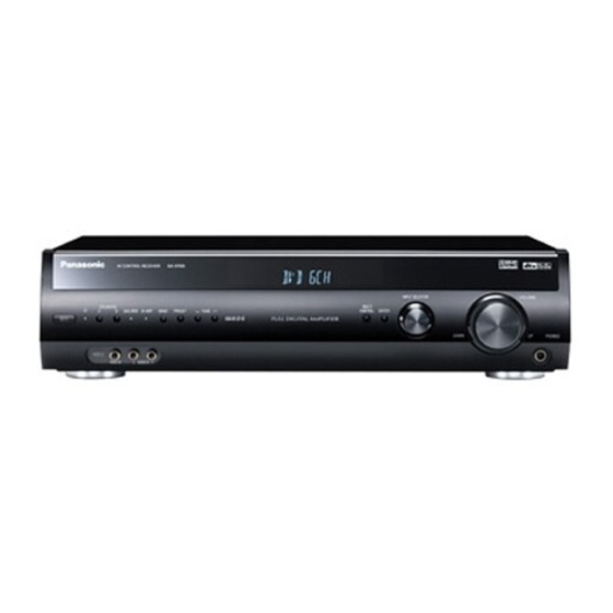
SA-XR55E / SA-XR55EB / SA-XR55EG
AMPLIFIER SECTION
Power output (at AC 230-240 V)
DIN 1 kHz (T.H.D. 1 %)
20 Hz-20 kHz continuous power
output both channels driven
Total harmonic distortion
rated power at 20 Hz-20 kHz
Power bandwidth
both channels driven, -3 dB
Power output each channel driven (at AC 230-240 V)
DIN 1 kHz (T.H.D. 1 %)
Front (L/R)
Center
Surround (L/R)
Surround Back (L/R)
Load impedance
Front (L/R)
A or B
A and B
BI-WIRE
ORDER NO. MD0505214C2
(K)...............Black Type (E/EG only)
Specification
2 x 100 W (6
2 x 80 W (6
4 Hz-88 kHz / (6
AV Control Receiver
(S)...............Silver Type
)
)
0.09 % (6
)
,
0.9 %)
100 W (6
)
100 W (6
)
100 W (6
)
100 W (6
)
6-16
6-16
6-16
Colour
Advertisement
Table of Contents

Related Manuals for Panasonic SA-XR55E


Summary of Contents for Panasonic SA-XR55E
- Page 1 ORDER NO. MD0505214C2 AV Control Receiver SA-XR55E / SA-XR55EB / SA-XR55EG Colour (S)....Silver Type (K)....Black Type (E/EG only) SPECIFICATIONS Specification AMPLIFIER SECTION Power output (at AC 230-240 V) DIN 1 kHz (T.H.D. 1 %) 2 x 100 W (6 20 Hz-20 kHz continuous power...
- Page 2 Center 6-16 Surround (L/R) 6-16 Surround Back (L/R) 6-16 Frequency response CD, TAPE, TV, DVD, DVD 4 Hz-88 kHz, ±3 dB RECORDER, VCR1, VCR2 DVD 6CH 4 Hz-44 kHz, ±3 dB Input sensitivity and impedance CD, TAPE, TV, DVD/DVD 6CH, DVD 200 mV/22 k RECORDER, VCR1, VCR2 S/N at rated power (6...
-
Page 3: Am Tuner Section
Stereo separation 1 kHz 40 dB Carrier leak 19 kHz -30 dB 38 kHz -50 dB Channel balance (250 Hz-6.3 kHz) ±1.5dB Limiting point Bandwidth IF amplifier 180 kHz FM demodulator 1000 kHz Antenna terminal (unbalanced) AM TUNER SECTION Frequency range 522-1611 kHz / (9 kHz step) 530-1620 kHz / (10... -
Page 4: Safety Precautions
2005 Matsushita Electric Industrial Co. Ltd.. All rights reserved. Unauthorized copying and distribution is a violation of law. 1. SAFETY PRECAUTIONS 1.1. GENERAL GUIDELINES 1. When servicing. observe the original lead dress. If a short circuit is found, replace all parts which have been overheated or damaged by the short circuit. -
Page 5: Caution For Ac Mains Lead
1.1.2. LEAKAGE CURRENT HOT CHECK (See Figure 1.) 1. Plug the AC cord directly into the AC outlet. Do not use an isolation transformer for this check. 2. Connect a 1.5k , 10 watts resistor, in parallel with a 0.15 capacitors, between each exposed metallic part on the set and a good earth ground such as a water pipe, as shown in Figure 1. -
Page 6: Before Repair And Adjustment
3. Before Repair and Adjustment Disconnect AC power, discharge Power Supply Capacitors C707, C717, C718 and C924 through a 10 , 10 W resistor to ground. DO NOT SHORT-CIRCUIT DIRECTLY (with a screwdriver blade, for instance), as this may destroy solid state devices. After repairs are completed, restore power gradually using a variac, to avoid overcurrent. -
Page 7: Handling The Lead-Free Solder
- No sound is heard when the power is turned on. - Sound stops during a performance. The function of this circuitry is to prevent circuitry damage if, for example, the positive and negative speaker connection wires are “shorted”, or if speaker systems with an impedance less than the indicated rated impedance of the amplifier are used. - Page 8 AC cord (For EB only) AC cord (For E/EG only) FM indoor antenna AM loop antenna...
-
Page 20: Other Connections
Antenna plug adaptor (For EB only) 7. Operating Instructions 7.1. Main Unit 7.2. Remote Control 7.3. Home Theater Connections 7.3.1. TV and DVD Player 7.3.2. Speakers 7.3.3. AC Power Supply Cord 7.4. Other Connections 8. Disassembly and Main Component Replacement Procedures and Operational Check “ATTENTION SERVICER”... -
Page 21: Disassembly Flow Chart
the respective procedures. / Special reassembly procedures are described only when required. 3. Select items from the following index when checks or replacement are required. - Disassembly of Top Panel - Checking for the DSP P.C.B. (Side A/B) and Main P.C.B. (Side - Disassembly and checking of Main P.C.B. -
Page 22: Disassembly Of Top Cabinet
8.3. Disassembly of Top Cabinet. Step 1 : Remove 4 screws from the top cabinet. Step 2 : Remove 3 screws from the rear panel. Step 3 : Lift up the top cabinet as arrow shown. - Page 23 Step 4 : Remove the top cabinet. 8.4. Checking for the DSP P.C.B. (Side A/B) and Main P.C.B. (Side A). - Follow the (Step 1) - (Step 4) of item 8.3. Step 1 : Check the DSP P.C.B. (Side A).
- Page 24 Step 2 : Remove 1 screw. Step 3 : Release the claws of the P.C.B support then detach the DSP. P.C.B. Step 4 : Flip over the DSP P.C.B. as arrow shown.
- Page 25 Step 5 : Connect the DSP P.C.B. (Side B) and Main P.C.B. / (Side A) by using the extension cable then proceed with the checking. 8.5. Disassembly and Checking of Main P.C.B. (Side B) - Follow the (Step 1) - (Step 4) of item 8.3. - Follow the (Step 1) - (Step 5) of item 8.4.
- Page 26 Step 3 : Detach the 25 pin FFC wire (REE1324) between / connectors P6501B (Main P.C.B.) and P6501A (Input P.C.B.) Step 4 : Flip over the Main P.C.B. as arrow shown. Step 5 : Check the Main P.C.B (Side B) by connecting the extension cable (RFKZ0317-25 pin). 8.6.
-
Page 27: Disassembly And Checking Of Speaker P.c.b
Step 1: Remove 2 screws. Step 2: Remove the tuner pack together with the Tuner Extent P.C.B. from the rear panel as arrow shown. Step 3: Detach the tuner pack from the Tuner Extent P.C.B. as arrow shown. 8.7. Disassembly and Checking of Speaker P.C.B. - Follow the (Step 1) - (Step 4) of item 8.3. - Page 28 Step 1: Remove 5 screws. Step 2: Remove the Speaker P.C.B. from rear panel as arrow shown for checking. 8.8. Disassembly and Checking of Component Video P.C.B. - Follow the (Step 1) - (Step 4) of item 8.3. Step 1: Remove 4 screws. Step 2: Remove the Component Video P.C.B.
- Page 29 Step 3: Flip over the Component Video P.C.B. as arrow shown for checking 8.9. Disassembly and Checking of Video & Optical P.C.B. - Follow the (Step 1) - (Step 4) of item 8.3. - Follow the (Step 1) - (Step 2) of item 8.6. - Follow the (Step 1) - (Step 3) of item 8.8.
-
Page 30: Disassembly Of Rear Panel
Step 2: Remove the Video & Optical P.C.B. from rear panel as arrow shown. Step 3: Flip over the Video & Optical P.C.B. as arrow shown for checking 8.10. Disassembly of Rear Panel - Follow the (Step 1) - (Step 4) of item 8.3. - Follow the (Step 1) of item 8.6. - Page 31 Step 1: Remove 11 screws. Step 2: Be careful of the both side catches when remove the rear panel. Step 3: Remove the rear panel as arrows shown.
- Page 32 8.11. Disassembly and Checking of Input P.C.B. - Follow the (Step 1) - (Step 4) of item 8.3. - Follow the (Step 1) of item 8.6. - Follow the (Step 1) of item 8.7. - Follow the (Step 1) of item 8.8. - Follow the (Step 1) of item 8.9.
-
Page 33: Disassembly Of Front Panel
Step 3: Proceed to check the Input P.C.B. 8.12. Disassembly of Front Panel - Follow the (Step 1) - (Step 4) of item 8.3. Step 1: Disconnect all the connectors (P951B, P902, P402, P303). - Page 34 Step 2: Be careful when remove the wires from the cord holder. Step 3: Remove 3 screws. Step 4: Release the both claws and remove the front panel as arrows shown. 8.13. Disassembly and Checking of Panel P.C.B., Volume P.C.B. and...
- Page 35 Headphone P.C.B. - Follow the (Step 1) - (Step 4) of item 8.3. - Follow the (Step 1) - (Step 4) of item 8.12. Step 1: Remove 5 screws. Step 2: Remove the front shield from the front panel as arrows shown Step 3: Remove 8 screws then remove the Panel P.C.B.
- Page 36 Step 4: Remove the Selector and Volume knobs. Step 5: Remove 3 screws then remove the Volume P.C.B. Step 6: Reconnect all the connectors and checking for Volume P.C.B., Panel P.C.B. and Headphone P.C.B. 8.14. Disassembly and Checking of Power P.C.B. - Follow the (Step 1) - (Step 4) of item 8.3.
- Page 37 - Follow the (Step 1) of item 8.7. - Follow the (Step 1) of item 8.8. - Follow the (Step 1) of item 8.9. - Follow the (Step 1) - (Step 3) of item 8.10. Steps 1 and 2: Remove 9 screws altogether. Step 3: Flip over the Power Supply P.C.B.
-
Page 38: Self Diagnosis Display Function
Step 4: Checking for Power P.C.B. 9. Self Diagnosis Display Function This unit is equipped with the self diagnosis display function, which alarms faulty operation with error code. Use this function during servicing. 9.1. Automatically Displayed Error Codes An error code automatically appears on the display (LCD) when faulty operation is detected. Refer to Fig. -
Page 39: Returning To Normal Display
LCD display Symptom Cause and Remedy OVERLOAD Speaker short, amplifier failure Speaker short and failure in power amplifier, pre-amplifier Humidity protection activated circuits. Check for faulty parts and replace with new parts if necessary. Communication error between Failure sub-micro processor sub micro- processor and its and its peripherals LSI. - Page 40 then press the [POWER] button at the same time. 2. The message, [SERVICE] appears on the display for three seconds, and then disappears. Refer to Fig. 9.2. Fig. 9.2 3. When the [TUNING DOWN] button is pressed, the current program filing number (ex.
- Page 41 The message, “_DOCTOR_” appears on the display for three seconds, and then disappears. Refer to Fig. 9.3. Fig. 9.3 3. Doctor mode function at some remote control codes as below table. Remote Test Mode Function and settings Control Selector Sound Mode other settings Vol/Tone CH 1...
-
Page 42: Voltage Measurement And Waveform Chart
LEVEL DVR/ STEREO Analog -18dB/0dB DVD_REC EFFECT STEREO Digital (COAX 2) -48dB/0dB STEREO Digital (OPT 1) -48dB/0dB SFC AV/ STEREO Digital (COAX 1) -48dB/0dB MOVIE SFC MUSIC DVR/ STEREO Digital (OPT 2) -48dB/0dB DVD_REC TEST No change SURROUND Scan the test noise output channel -18dB/0dB with 500ms intervals STEREO... -
Page 43: Voltage Measurement
10.1. Voltage Measurement 10.1.1. DSP P.C.B. 10.1.2. Main P.C.B. 10.1.3. Input P.C.B. 10.1.4. Panel P.C.B. 10.1.5. Power P.C.B. 10.1.6. Video & Optical P.C.B. 10.1.7. Component Video P.C.B. 10.2. Waveform Chart 11. Block Diagram 12. Notes of Schematic Diagram (All schematic diagrams may be modified at any time with the development of new technology) Note : S901 Power switch... -
Page 44: Schematic Diagram
S910 Enter switch VR901 Volume VR902 Input Selector - The voltage value and waveforms are the reference voltage of this unit measured by DC electronic voltmeter (high impedance) and oscilloscope on the basis of chassis. Accordingly, there may arise some error in voltage values and waveforms depending upon the internal impedance of the tester or the measuring unit. - Page 45 IC507 6(25) 26(5) JK404 C0ABBB000125 DVR IN OP AMP 27(4) JK403 DVD IN L/R Q503 28(3) JK402 TAPE PLAY IN MUTING SWITCH 29(2) JK401 9(22) 24(7) JK405 VCR1 IN 23(8) JK405 TV / STB IN 21(10) TUNER PACK 20(11) 12(19) JK901 VCRIN2_L (VCRIN2_R)
- Page 46 SYSCK SDATA IC508 IC509 IC1011 4(25) AINL+ BCLK C1BB00000672 C0ABBB000102 C0ABBB000102 (AINR+) MULTI-BIT AUDIO OP AMP OP AMP A/D CONVERTER LRCK D1006 OVFL QR1003 5(24) D1005 AINL- (AINR-) SWITCH OVFR OSR0 OSR1 /RST SYSCK SDATA BCLK 4(25) AINL- (AINR-) LRCK D1004 OVFL IC1010...
- Page 47 MCLK_AD DAUX BCLK_AD BCLK BLCK BCLK_AD LRCK_AD IC1008 LB1012 TVDD TVDD C1BB00000692 LRCK LRCK DIGITAL AUDIO DIRINT1 INTERFACE INT1 LRCK_AD OVF_F TRANSCEIVER DIRINT0 INT0 JK409 OPTICAL INPUT 1 QR1001 DVR IN SWITCH JK410 OSC_PW OPTICAL INPUT 2 TV/STB IN IC499 C0JBAB000685 IC1005 JK412...
- Page 48 OSC_PV IOPORT1 OSR0 IOPORT2 OSR1 AU0B SDOBCK IOPORT3 AU1B /AD_RST SDOWDCK IOPORT4 AU2B OVF_F SCOMCK IOPORT5 AU3B OVF_S SDO0 IOPORT6 MCLKB SDO1 BCLKB ADOUT1 SDO2 SDI1 LRCLKB ADOUT2 SDO3 SDI2 IC6671 SDATA C0JBAZ001539 SDI0 LOGIC GATE IC IC1007 MCLK SDIMCK C2HBCK000001 DSP_nMUTE nMUTE...
- Page 49 D6862 /MUT_SW QR6851 QR6852 SWITCH SWITCH D6852 /AF_MUTE D6851 Q6871 QR6861 QR6862 SWITCH SWITCH SWITCH IC6701 D6861 C1BB00000834 6CH PWM PROCESSOR IC6602 C0JBAA000244 STANDARD GATE IC Q6001 (Q6003) HPL_P 4A(2B) 12(5) 45(50) AP_6(AP_5) 4Y(2Y) 11(6) 3(5) SWITCH FILTER VAL_ID_SW 13(4) 4B(2A) MCLKB IC6051...
- Page 50 JK407 SUBWOOFER IC6971 C0DBEKG00004 REGULATOR JK903 IC6972 HEADPHONE C0DBEKG00004 Q6005 REGULATOR (Q6006) L999 (L998) SWITCH IC6001 C0DBEKG00004 REGULATOR D6813 Q6081 Q6810 Q6809 QR6811 D6814 SWITCH SWITCH SWITCH SWITCH Q6807,Q6808 SWITCH QR6805 SWITCH D6474 QR6806 SWITCH Q6451 AMPLIFIER C+ CH JK602 CENTRE SPEAKER C- CH...
- Page 51 49(37) DHS_A (DHS_C) IC6301 IC6601 51(39) C1BB00000835 GHS_A C1BB00000834 (GHS_C) DUAL H-BRIDGE 6CH PWM PROCESSOR DRIVER 52(40) SHS_A (SHS_C) 50(38) BST_A (BST_C) /RST_CD VALID_2 GLS_A 54(42) /RST_AB VALID_1 (GLS_C) 43(31) DHS_B 10(15) 75(70) (DHS_D) AP_1(2) AP(CP) 74(69) 11(16) 45(33) AM_1(2) AM(CM) GHS_B (GHS_D)
- Page 52 RLY606(RLY605) SL+CH(SR+CH) Q6301 (Q6351) JK601 SURROUND BACK SL-CH(SR-CH) SPEAKER L(R) SWITCH QR6301 D6325 (D6375) (QR6351) SWITCH D6324 (D6374) RLY606(RLY605) Q6302 (Q6352) SWITCH QR6302 (QR6352) SWITCH Q884 SWITCH D6224 (D6274) Q6201 (Q6251) AMPLIFIER RLY603 SL+CH(SR+CH) JK602 SURROUND SPEAKER L(R) D6225 (D6275) SL-CH(SR-CH) QR6201 Q6202...
- Page 53 M2S_DT_S REQM_3 IC6904 C0JBAA000244 REQL_5 STANDARD GATE IC M2S_DT_5 TO TUNER PACK NAND MCK_3 S2M_DT_5 IC6903 REQS_5 X201 C0JBAA000175 REQS_3 LOGIC IC MCK_5 nMUTE IC201 C1BB00000987 /MUTE MPXIN IC6801 C2BBGF000669 MAIN MICRO-P 37(33) QR6801 RESET SWITCH Q6802 SWITCH IC6802 C3EBCG000031 EEPROM (NOT SUPPLIED)
- Page 54 QR901, QR903, QR905 FROM POWER FL901 SWITCH TRANSFORMER FL DISPLAY QR902, QR904, QR906 17~39 SWITCH FL3~FL25 D999, QR907, D907, D998, QR911, D906, D997 QR909 D904 2,1,40 FL0, FL26, SEL_DATA SWITCH FL1, FL27, IC901 FL29 C0HBB0000044 SEL_CLK FL DRIVER SEL_STB VCR_REC TAPE_REC_MUTE BEAT_PROOF VR902...
- Page 55 JK302 VCR IN VIDEO JK302 DVD REC IN IC303 C1AB00001931 VIDEO SELECTOR JK901 VCR2 IN JK301 DVD REC OUT JK301 VIDEO DVD IN JK302 TV/STB IN JK301 TV MONITOR JK303 DVD IN IN4 S3 IC301 C1AB00001931 JK304 VIDEO SELECTOR DVD REC IN JK304 TV/STB IN JK303...
- Page 56 SIGNAL LINES : MAIN SIGNAL LINE : FM/AM SIGNAL LINE : VIDEO SIGNAL LINE ) Indicates Pin No. of Right Channel Note : Signal Lines are applicable to the Left Channel only. IC304 C1AB00002029 SW AMP IC JK306 CH1 IN2 DVD IN CH2 IN2 PSave...
- Page 57 C0JBAA000244 (14p) C0JBAF000540(6p) C0JBAB000702 C3BBHC000348(32p) C0ABBB000125(8p) C0JBAR000400(8p) C0JBAB000710 C1BB00000835(56p) C1AB00002029(24p) C1AB00001931(16p) C0JBAA000175(14p) C0ABBA000073(8p) C0JZAS000004(30p) C0JBAZ001539(20p) C1BB00000987(16p) C1BB00000672(28p) C0JBAB000633(8p) C0JBAB000685(6p) C0DBEKG00004 C1BB00000692 (48p) C0EAS0000032 C5HABZZ00125 C1BB00000834(80p) C0HBB0000044(40p) C2CBJG000650(100p) C2BBGF000669 (64p) C2HBCK000001(144p) C0DACZZ00007 B1GACFJN0007 B1GFGCAA0001 C0AABB000129 B1DEGF000004 C0ABBB000102 MIP2C10MPSCF B1ABEC000010 2SD0592AWA B1AAGC000006 B1BACJ000005 B1GDCFJN0001 B1DEGL000008...
- Page 58 DSP P.C.B (REP3890A-T) CN1002 CN1003 R1089 C1090 C1086 C1089 CN1001 C1081 R1059 C1094 R1070 C1039 C1023 C1042 C1049 C1047 R1069 C1022 R1045 C1095 R1067 R1068 R1044 R1066 R1043 R1065 R1042 LB1011 R1064 R1038 R1037 C1036 R1036 R1035 IC1007 C1055 C1054 C1053 X1001 C1024...
- Page 59 DSP P.C.B (REP3890A-T) CN1004 C1078C1079 C1074 C1060 C1070 C1071 C1062 C1063 C1076 C1058 IC1011 IC1010 IC1009 D1005 QR1003 D1006 D1004 D1003 QR1002 C1048 C1015 LB1013 C1020 C1021 R1056 C1019 LB1012 R1054 C1018 R1055 R1014 R1011 R1058 R1026 IC1008 R1010 C1027 R1013 R1009 C1028...
- Page 60 INPUT P.C.B (REP3889B-S) AUDIO JK402 JK401 JK403 JK404 JK407 C418 R418 C445 C426 C417 C425 C421 R402 C401 C436 C420 R423 R410 R409 R411 R414 R413 C434 C428 C424 R416 R412 C427 R415 D402 Q404 R424 C432 R428 C410 R405 Q402 Q401 C412...
- Page 61 JK404 JK405 Q501 C442 C443 C508 R512 R418 R514 C426 C433 C425 C437 C436 R502 C441 C444 R422 R414 R413 R417 R419 R504 C510 C434 W158 C502 C503 C428 C440 R416 R501 R511 C439 C427 R415 R507 C501 W100 C505 R532 C507 R513...
- Page 62 MAIN P.C.B (REP3888B-M) R6858 TH6101 R6857 R6168 R6166 C6170 C6179 R6164 C6158 R6179 C6169 C6168 R6141 C6154 C6177 R6177 IC6101 D6175 C6116 R6114 C6108 C6129 QR6152 C6118 C6112 C6120 R6129 R6112 QR6151 C6119 C6115 C6172 QR6102 QR6101 D6174 C6122 D6124 R6125 D6125 C6266...
- Page 63 IC6971 R6168 D6872 C6179 C6872 R6179 C6169 R6142 R6871 C6141 Q6802 C6168 R6141 QR6801 D6101 X6801 C6177 R6177 IC6101 R6833 R6834 R6816 R6817 R6835 R6815 R6873 R6836 R6814 R6813 R6837 C6129 R6812 C6118 C6112 R6838 R6811 R6810 R6129 C6844 R6839 R6809 IC6801 R6808...
- Page 64 MAIN P.C.B (REP3888B-M) P606 Q6152 C6152 Q6151 Q6102 C6102 C6101 Q6101 P601 Q6252 C6252 C6251 Q6251 Q6202 C6202 C6201 P602 Q6201 Q6352 C6352 C6351 Q6351 C6302 Q6302 C6301 P603 Q6301 C6452 Q6452 C6451 Q6451 P605B (SIDE B)
- Page 65 P6501B Q6152 Q6151 P906 Q6102 15 16 17 18 19 20 21 22 23 24 25 13 12 11 10 Q6101 Q6252 Q6251 Q6202 Q6201 Q6352 Q6351 Q6302 Q6301 Q6452 IC6051 Q6451 P951B...
-
Page 66: Digital-In
VIDEO & OPTICAL P.C.B (REP3889B-S) DIGITAL IN VIDEO JK409 JK410 JK301 JK412 C328 L315 R301 L301 R334 C499 C498 C301 L499 L498 L497 W323 C488 L496 W308 W302 W303 C489 W305 C490 IC303 R498 R499 12 10 R497 R496 C494 C495 C493 C492... - Page 67 VIDEO S-VIDEO JK302 JK301 JK304 JK303 R301 L312 L313 R330 L309 R328 R315 L301 W368 C301 L306 L305 R318 C310 R307 R310 R311 R316 W323 C317 W353 IC303 W354 C313 R320 W318 W360 IC302 IC301 W319 C365 W372 W369 C319 W347 W346 D301...
- Page 68 PANEL P.C.B (REP3889B-S) D909 L908 P951A L904 9 11 13 15 17 10 12 14 16 L903 W205 W206 W202 W203 FL901 JW902A QR901 QR903 QR905 R942 R943 C922 R944 IC901 W244 W245 W246 R912 QR904 QR906 QR902 R913 C929 R939 C927 R941...
- Page 69 JW903 D902 QR911 QR909 QR907 R908 IC901 R913 S901 POWER C927 R941 R914 S903 S908 S907 S904 S906 S902 BAND SPEAKER B TUNE UP TUNE DOWN PRESET SPEAKER A R915 R916 R904 JK901 L914 C933 C905 R907 C903 C904 C935 C901 R903 R901...
- Page 70 230V 50Hz...E/EG POWER P.C.B (REP3891C-P) 230V-240V 50Hz...EB AC IN W214 W322 W323 W223 RY604 W407 P701 W317 W406 RY605 W316 W315 W318 P622 W219 W314 R883 P621 Q882 D885 B C E L701 W218 RY606 B C E JW601 W320 JW401 Q881 JW602...
- Page 71 VOLUME P.C.B (REP3889B-S) JW902B C987 C989 VR902 ZJ992 C985 C986 VR901 INPUT VOLUME SELECTOR SPEAKER P.C.B (REP3891C-P) SPEAKERS 1+SL 3+SR 1+SL 3+SR 8+FL 1+FR 3+FL 6+FR JK601 JK602 JK603 JW622B JW621B JW603...
-
Page 72: Schematic Diagram
SCHEMATIC DIAGRAM - 1 SIDE A SIDE B DSP CIRCUIT : +B SIGNAL LINE :MAIN SIGNAL LINE C1027 100P C1028 100P R1058 C1029 100P C1030 100P +3.3VD C1036 LB1011 16V10 JOJHC0000021 C1051 INT1 LRCK C1031 AVDD MCK01 R1049 DVSS C1032 0.47 VCOM DVDD IC1008... - Page 73 SCHEMATIC DIAGRAM - 2 DSP CIRCUIT : +B SIGNAL LINE :MAIN SIGNAL LINE R1076 R1078 R1071 R1073 C1064 C1072 C1062 R1075 C1070 R1080 470P 470P IC1009 IC1010 C1BB00000672 C1BB00000672 MULTI-BIT AUDIO A/D CONVERTER MULTI-BIT AUDIO A/D CONVERTER C1063 C1071 470P 470P C1073 C1065...
- Page 74 SCHEMATIC DIAGRAM - 3 DSP CIRCUIT : +B SIGNAL LINE :MAIN SIGNAL LINE CN1001 DIG GND 3.3VD DIG GND DIG GND VIDEO & OPTICAL DIG GND CIRCUIT (P302) ON DIG GND SCHEMATIC DIAGRAM-38 DIG GND DIG GND CN1002 AINC+ AINC+ AINC- AINC- AGND...
- Page 75 SCHEMATIC DIAGRAM - 4 DSP CIRCUIT : +B SIGNAL LINE :MAIN SIGNAL LINE LB1007,LB1008 J0JHC0000021 LB1008 LB1007 LB1006 LB1005 J0JHC0000021 J0JHC0000021 C1015 C1017 6V47 C1021 C1020 C1018 C1022 AHVSS VDD2 AHVSSG VDD2 C1024 DVSS DVD0 VDD2 MEMD7 VDD2 MEMD6 MEMD5 MEMD4 C1038 1 VDD1...
- Page 76 SCHEMATIC DIAGRAM - 5 DSP CIRCUIT : +B SIGNAL LINE IC1003 C3BBHC000348 SDRAM IC MA11 /MOE MA10 C1014 6V47 /MCE /CE1 MA13 R1005 C1016 R1006 6V47 /MWE R1007 R1008 R1009 R1010 R1002 MA15 R1011 R1012 IC1003 R1013 /MCE MA16 R1014 /MOE R1015 /MWE...
-
Page 77: Main Circuit
INPUT CIRCUIT SCHEMATIC DIAGRAM -6 (P6501A) ON SCHEMATIC SIDE A SIDE B : + B SIGNAL LINE DIAGRAM-28 MAIN CIRCUIT : MAIN SIGNAL LINE P6501B 15 14 13 12 11 10 SEL_ENCA LB6815 SEL_ENCB LB6814 KEY2 LB6813 KEY1 LB6812 ENC2 ENC2 LB6811 +5VD... - Page 78 SCHEMATIC DIAGRAM -7 :-B SIGNAL LINE MAIN CIRCUIT :+ B SIGNAL LINE : MAIN SIGNAL LINE R6889 R6841 R6890 C6844 0.001 R6849 R6832 F_OE TAPE_REC R6850 R6831 OSD_STB FL/LED_CK R6851 R6830 OSD_DATA FL/LED_DT R6852 R6829 OSD_CLK FL_ST R6828 R6853 FLD_RESET VCR_REC R6827 R6854...
- Page 79 SCHEMATIC DIAGRAM -8 :-B SIGNAL LINE MAIN CIRCUIT :+ B SIGNAL LINE : MAIN SIGNAL LINE R6969 R6970 C6962 R6968 R6967 R6200 R6500 R6946 R6961 /DSP_CS R6945 -DIR_CS /DIR_CS -DIR_RST R6944 /DIR_RESET R6963 ZERO_FLG R6941 IC6901 ZEROFLG R6940 C2CBJG000650 nMUTE R6939 REQS_3 SUB MICRO-P...
- Page 80 SCHEMATIC DIAGRAM -9 :-B SIGNAL LINE MAIN CIRCUIT :+ B SIGNAL LINE : MAIN SIGNAL LINE IC6904 IC6903 C0JBAA000175 C0JBAA000244 LOGIC IC LOGIC IC /DSP_CS C6923 C6922 0.01 0.01 IC6972 IC6971 C0DBEKG00004 C0DBEKG00004 REGULATOR IC REGULATOR IC SCDCLK SDIN SDOUT R6916 F10K R6980...
- Page 81 SCHEMATIC DIAGRAM -10 :-B SIGNAL LINE MAIN CIRCUIT :+ B SIGNAL LINE : MAIN SIGNAL LINE R6895 C6096 6.3V1000P Q6871 C6994 C6995 C6996 Q6871 C6988 B1CBGD000001 SWITCH C6989 C6990 LB6701 J0JGC0000017 C6991 PWM_RST VOLCNT -DSP_RST -DSP_CS ZERO_FLG -DSP_INT DIR_INT1 DIR_INT0 SDIN -DIR_RST SCDCLK...
- Page 82 SCHEMATIC DIAGRAM -11 :-B SIGNAL LINE MAIN CIRCUIT :+ B SIGNAL LINE : MAIN SIGNAL LINE R6089 IC6082 C0AABB000129 C6075 C6076 C6080 R6046 R6045 OP AMP IC 50V2.2 3.3K 3.3K R6048 R6047 3.3K 3.3K R6050 R6049 C6085 3.3K 3.3K R6083 R6055 3.3K C6090...
- Page 83 SCHEMATIC DIAGRAM -12 :-B SIGNAL LINE MAIN CIRCUIT :+ B SIGNAL LINE : MAIN SIGNAL LINE R6042 R6041 C6042 C6046 C6047 C6041 C6045 C6048 R6027 R6028 R6007 R6008 50V2.2 50V2.2 3.3K 3.3K 3.3K 3.3K R6029 R6030 R6009 R6010 3.3K 3.3K 3.3K 3.3K R6087...
- Page 84 SCHEMATIC DIAGRAM -13 :-B SIGNAL LINE MAIN CIRCUIT :+ B SIGNAL LINE : MAIN SIGNAL LINE D+15V DIG2 PVDD DIG2 IC6051 C0AABB000129 Q6005,Q6006 B1GFGCAA0001 OP AMP IC MUTING SWITCH R6069 C6059 R6061 R6063 C6019 16V47 HP_L R6073 C6056 R6071 R6065 R6067 C6055 C6054...
- Page 85 SCHEMATIC DIAGRAM -14 MAIN CIRCUIT :+ B SIGNAL LINE : MAIN SIGNAL LINE R6780 C6779 16V10 R6779 C6760 VREGP_CAP C6759 DVDD_SCL R6703 MCLK_IN DVSS_SCL C6757 ADVV_PLL DVDD_PWM PLL_FLT_OUT DVSS_PWM R6755 SW_P PLL_FLT_DET AP_4 AVSS_PLL AM_4 R6753 VAL ID_SW C6709 VALID_4 VREGA_CAP BM_4 R6751...
- Page 86 SCHEMATIC DIAGRAM -15 MAIN CIRCUIT :+ B SIGNAL LINE : MAIN SIGNAL LINE AP_7 DIG2 DIG2 AM_7 DIG2 VALID_7 C (EXT) CH BM_7 DIG2 BP_7 DIG2 AP_9 DIG2 AM_9 DIG2 C CH VALID_9 DIG2 BM_9 DIG2 DIG2 BP_9 DIG2 AP_1 AM_1 DIG2 VALID_1...
- Page 87 SCHEMATIC DIAGRAM -16 MAIN CIRCUIT : +B SIGNAL LINE : MAIN SIGNAL LINE IC6001 IC6001 C0DBEKG00004 REGULATOR IC R6078 R6079 100K GND OUT LB6001 J0JGC0000017 DIG1 D+15V C6077 C6078 R6077 C6079 25V33 25V33 DIG1 +3.3VPWM R6401 IC6401 C1BB00000835 DIGITAL AMP POWER STORAGE CONTROLLER C6418 GVSS...
- Page 88 SCHEMATIC DIAGRAM -17 : +B SIGNAL LINE MAIN CIRCUIT : MAIN SIGNAL LINE POWER CIRCUIT SPEAKER CIRCUIT (JW606) ON (JW603) ON SCHEMATIC SCHEMATIC DIAGRAM-32 DIAGRAM-31 P606 P603 DIG1 PVDD C6481 C6482 1000P 1000P L6453 C6458 C6457 D6453 0.01 L6451 G0C7R0K00003 R6467 R6457 C6451...
- Page 89 SCHEMATIC DIAGRAM -18 MAIN CIRCUIT : +B SIGNAL LINE : MAIN SIGNAL LINE Q6301,Q6302 B1DEGF000004 AMPLIFIER R6301 IC6301 C1BB00000835 DIGITAL AMP POWER STORAGE CONTROLLER Q6301 GVSS R6318 R6303 GVDD DVDD GLS_A R6305 DVSS SLS_A R6302 C6342 SHS_A R6331 DTC_HS GHS_A C6305 Q6302 R6332...
- Page 90 SCHEMATIC DIAGRAM -19 MAIN CIRCUIT : +B SIGNAL LINE : MAIN SIGNAL LINE L6303, 6304 G0C50NZ00001 D6303, 6304 B0JCMG000016 L6303 C6303 C6304 C6308 1000P 50V1000 C6307 D6303 0.01 L6301 G0C7R0K00002 R6315 R6317 R6307 C6327 330P C6301 R6312 0.47 4.7K C6315 C6317 R6308 R6327...
- Page 91 SCHEMATIC DIAGRAM -20 MAIN CIRCUIT : +B SIGNAL LINE : MAIN SIGNAL LINE Q6201,Q6202 B1DEGF000004 D6203, 6204 B0JCMG000016 AMPLIFIER R6201 L6203 IC6201 G0C50NZ00001 C1BB00000835 DIGITAL AMP POWER STORAGE CONTROLLER Q6201 GVSS R6218 R6203 GVDD DVDD GLS_A R6205 DVSS SLS_A C6242 R6202 SHS_A R6231...
- Page 92 SCHEMATIC DIAGRAM -21 MAIN CIRCUIT : +B SIGNAL LINE : MAIN SIGNAL LINE L6203, 6204 G0C50NZ00001 L6203 QR6301, QR6302, QR6351, QR6352 C6208 B1GBCFQQ0002 C6207 D6203 SWITCH 0.01 L6201 G0C7R0K00003 QR6301 C6323 D6324 R6321 R6217 330P 220K B0ACCK000005 R6207 C6201 R6323 0.47 R6324 C6217...
- Page 93 SCHEMATIC DIAGRAM -22 MAIN CIRCUIT : +B SIGNAL LINE : MAIN SIGNAL LINE Q6101,Q6102 B1DEGF000004 R6101 IC6101 AMPLIFIER C1BB00000835 DIGITAL AMP POWER STORAGE CONTROLLER GVSS R6118 R6103 GVDD Q6101 DVDD GLS_A R6105 DVSS SLS_A R6102 C6142 SHS_A R6131 DTC_HS GHS_A C6105 R6132 0.022...
- Page 94 SCHEMATIC DIAGRAM -23 MAIN CIRCUIT : +B SIGNAL LINE : MAIN SIGNAL LINE L6303, 6304 G0C50NZ00001 D6303, 6304 B0JCMG000016 L6103 C6108 C6107 D6103 0.01 L6101 G0C7R0K00003 R6117 R6107 C6101 0.47 C6117 R6108 POWER CIRCUIT 0.01 QR6101 C6123 (JW601) ON D6124 R6121 330P B0ACCK000005...
-
Page 95: Tuner Pack
SCHEMATIC DIAGRAM -24 : -B SIGNAL LINE : FM/AM SIGNAL LINE INPUT CIRCUIT : +B SIGNAL LINE : MAIN SIGNAL LINE SEL_CLK SEL_CLK SEL_CLK RDS_CLK TU_ST TU_ST TUN_ST RDS_DATA SEL_DATA SEL_DATA SEL_DATA TUNER_L TUNER_L TUN_CE TUN_CE TUN_CE TUNER_R TUNER_R TUNER PACK (RAN0002EM-1) DC_DET_+7V TUN_SD... - Page 96 SCHEMATIC DIAGRAM -25 : -B SIGNAL LINE : FM/AM SIGNAL LINE INPUT CIRCUIT : +B SIGNAL LINE : MAIN SIGNAL LINE L201 J0JBC0000041 C208 10V47 R201 100K R202 100K C205 0.01 C202 R204 +5VD IC201 C1BB00000987 RDS IC C210 C209 C207 16V47 16V10...
- Page 97 SCHEMATIC DIAGRAM -26 : -B SIGNAL LINE INPUT CIRCUIT : +B SIGNAL LINE : MAIN SIGNAL LINE R508 3.3K R502 C504 25V10 DVD_SW Q501 R510 1.8K B1GFGCAA0001 MUTING SWITCH C502 R504 R506 C506 100P 100K IC501 C0ABBB000125 OP AMP IC C505 C501 R503...
- Page 98 SCHEMATIC DIAGRAM -27 : -B SIGNAL LINE INPUT CIRCUIT : +B SIGNAL LINE : MAIN SIGNAL LINE AD_SWIN- C508 R512 R514 R516 R518 25V10 8.2K 4.7K R520 C510 C512 330P 150P AD_SWIN+ C515 C514 R521 C513 25V10 IC502 IC503 C0ABBB000102 C0ABBB000102 OP AMP IC OP AMP IC...
- Page 99 SCHEMATIC DIAGRAM -28 : -B SIGNAL LINE INPUT CIRCUIT : +B SIGNAL LINE : MAIN SIGNAL LINE Q505 B1ABEC000010 SWITCH R576 R577 R578 1.5K BEAT_PROOF Q505 QR502 QR503 B1GDCFJJ0008 UNR211500L P6501A CONTROL SWITCH R579 SWITCH (ATTENUATION) 820K R582 2.2K C559 R581 R583 100K...
- Page 100 SCHEMATIC DIAGRAM -29 : -B SIGNAL LINE PANEL CIRCUIT : +B SIGNAL LINE FL901 A2BB00000139 FL DISPLAY 7 8 9 10 11 12 13 14 15 16 17 18 19 20 21 22 23 24 25 26 27 28 29 30 31 32 33 34 35 36 37 38 39 40 41 42 43 44 48 49...
- Page 101 SCHEMATIC DIAGRAM -30 : -B SIGNAL LINE : MAIN SIGNAL LINE PANEL CIRCUIT : +B SIGNAL LINE : VIDEO SIGNAL LINE QR902,QR904 QR901,QR903 B1GACFGG0004 B1GCCFJJ0008 SWITCH SWITCH R940 JW903 +5.2V QR903 QR901 FL_0V FL_+5V POWER CIRCUIT R910 R909 (P902) ON 100K 100K SCHEMATIC...
-
Page 102: Speaker Circuit
SCHEMATIC DIAGRAM -31 SPEAKER CIRCUIT :MAIN SIGNAL LINE +(SURROUNDBACK_L) SURROUND BACK -(SPEAKER_SBL) SPEAKER LEFT +(SURROUNDBACK_R) SURROUND BACK -(SPEAKER_SBR) SPEAKER RIGHT POWER CIRCUIT (P621) ON JK601 SCHEMATIC DIAGRAM-35 JW621B +(SURROUND_L) SURROUND -(SPEAKER_L) SPEAKER LEFT +(SURROUND_R) SURROUND -(SPEAKER_R) SPEAKER RIGHT +(CENTER) CENTER MAIN CIRCUIT -(SPEAKER_C) SPEAKER... - Page 103 SCHEMATIC DIAGRAM -32 : -B SIGNAL LINE POWER CIRCUIT : +B SIGNAL LINE Q733 B1GBCFJA0002 REGULATOR -15V D735-D736 D737 B0HAJL000001 +5VA B0HAJL000001 R746 R747 Q733 T731 D745 120K C745 ETS28AU2V9AC C744 R800 B0EAKM000122 1000P 1000P FP701 R744 R743 C757 R745 D736 50V4.7 DCDET...
- Page 104 SCHEMATIC DIAGRAM -33 : -B SIGNAL LINE POWER CIRCUIT : +B SIGNAL LINE T721 D721 ETS19AB1X6AG R771 B0HAJL000001 D715 D723 B0EDKT000009 B0JAJG000002 BK+5R7V C725 250V4.7 R775 C730 C727 R773 10V220 470K C729 50V1 IC721 C726 R772 MIP2C10MPSCF 1800P 100K SWITCHING IC D724 D722 MAZ80470ML...
- Page 105 SCHEMATIC DIAGRAM -34 POWER CIRCUIT : +B SIGNAL LINE : MAIN SIGNAL LINE RY601 K6B2AGA00011 Q881 R881 3.3K SP_A D881 Q881, 882 B0ACCK000005 B1AAGC000006 SWITCH RY602 K6B2AGA00011 Q882 R883 3.3K SP_B D882 B0ACCK000005 D884 B0EAKM000122 +15V R888 D728 D701 B0ACCK000005 MDRIVE Q884 B0FFKC000001...
- Page 106 SCHEMATIC DIAGRAM -35 POWER CIRCUIT : +B SIGNAL LINE : MAIN SIGNAL LINE P621 SBL+ SBL- SBR+ SBR- SPEAKER CIRCUIT (JW621B) ON SCHEMATIC DIAGRAM-31 P622 FBL+ FBL- FBR+ FBR- SPEAKER CIRCUIT FAL+ (JW622B) ON FAL- SCHEMATIC DIAGRAM-31 FAR+ FAR- RY605 K6B2CGA00086 RY605 JW601...
- Page 107 SCHEMATIC DIAGRAM -36 : -B SIGNAL LINE : +B SIGNAL LINE : VIDEO SIGNAL LINE VIDEO & OPTICAL CIRCUIT JK304 L310,311 J0JBC0000033 C312 C365 C313 C311 16V47 L311 R319 R317 R365 R320 TV/STB IN GND 03 C310 0.022 L310 R316 R318 IC301 C1AB00001931...
-
Page 108: Panel Circuit
SCHEMATIC DIAGRAM -37 : -B SIGNAL LINE : +B SIGNAL LINE : VIDEO SIGNAL LINE VIDEO & OPTICAL CIRCUIT C315 6V100 VGND C314 R323 D301 INPUT CIRCUIT MA2J11100L R324 (P304A) ON SCHEMATIC R325 DIAGRAM-28 D302 MA2J11100L JW304B C320 6V100 VGND PANEL CIRCUIT VCR2_S_VIDEO_Y (JW904) ON... - Page 109 SCHEMATIC DIAGRAM -38 VIDEO & OPTICAL CIRCUIT : +B SIGNAL LINE : MAIN SIGNAL LINE DIG_GND JK409 R491 OUTPUT 3.3VD OPTICAL INPUT 1 L499 VLQ0855M1R0T (DVR IN) C499 DSP CIRCUIT (CN1001) ON SCHEMATIC JK410 DIAGRAM-3 R492 OUTPUT OPTICAL INPUT 2 (TV/STB IN) C498 P302...
-
Page 110: Input Circuit
SCHEMATIC DIAGRAM -39 : -B SIGNAL LINE COMPONENT VIDEO CIRCUIT : +B SIGNAL LINE : VIDEO SIGNAL LINE JK308 C391 R394 C392 TV/STB R395 C393 R396 C395 C388 JK307 C394 C396 R391 C389 DVD REC C398 R392 6V100 C390 VGND INPUT CIRCUIT R393 (P301) ON... - Page 111 COMPONENT VIDEO P.C.B. IC304 Ref No. MODE CD PLAY -5.1 -5.1 STANDBY IC304 Ref No. MODE CD PLAY STANDBY...
- Page 112 DSP P.C.B. IC1001 Ref No. MODE CD PLAY STANDBY IC1002 Ref No. MODE CD PLAY STANDBY IC1003 Ref No. MODE CD PLAY STANDBY IC1003 Ref No. MODE CD PLAY STANDBY IC1005 Ref No. MODE CD PLAY STANDBY IC1006 Ref No. MODE CD PLAY STANDBY...
- Page 113 IC1008 Ref No. MODE CD PLAY STANDBY IC1008 Ref No. MODE CD PLAY STANDBY IC1008 Ref No. MODE CD PLAY STANDBY IC1009 Ref No. MODE CD PLAY STANDBY IC1009 Ref No. MODE CD PLAY STANDBY IC1010 Ref No. MODE CD PLAY STANDBY IC1010 Ref No.
- Page 114 INPUT P.C.B. IC201 Ref No. MODE CD PLAY STANDBY IC402 Ref No. MODE CD PLAY -14.8 STANDBY -0.2 IC402 Ref No. MODE CD PLAY 15.0 STANDBY IC501 Ref No. MODE CD PLAY -14.8 15.0 STANDBY IC502 Ref No. MODE CD PLAY STANDBY IC503 Ref No.
- Page 115 MAIN P.C.B. IC6001 Ref No. MODE CD PLAY 15.0 15.0 12.0 STANDBY IC6051 Ref No. MODE CD PLAY -15.1 15.0 STANDBY IC6082 Ref No. MODE CD PLAY -15.1 15.0 STANDBY IC6101 Ref No. MODE CD PLAY STANDBY IC6101 Ref No. MODE CD PLAY 12.0...
- Page 116 IC6602 Ref No. MODE CD PLAY STANDBY IC6603 Ref No. MODE CD PLAY STANDBY IC6671 Ref No. MODE CD PLAY STANDBY IC6701 Ref No. MODE CD PLAY STANDBY IC6701 Ref No. MODE CD PLAY STANDBY IC6701 Ref No. MODE CD PLAY STANDBY IC6701 Ref No.
- Page 117 IC6971 Ref No. MODE CD PLAY STANDBY IC6972 Ref No. MODE CD PLAY STANDBY Q6001 Q6002 Q6003 Q6004 Q6148 Ref No. MODE CD PLAY STANDBY Q6005 Q6006 Q6081 Ref No. MODE CD PLAY -6.1 -6.1 -6.1 -6.1 -6.2 -6.2 STANDBY Q6091 Q6092 Q6101...
- Page 118 PANEL P.C.B. IC901 Ref No. MODE CD PLAY -27.8 -27.8 -30.5 5.0 -30.5 -30.5 -30.5 -30.5 -27.5 -24.7 -24.7 STANDBY IC901 Ref No. MODE CD PLAY -30.5 -27.5 -30.5 -24.7 -27.5 -27.5 -27.5 -30.5 -24.7 -30.5 -24.7 -27.5 -27.5 -27.5 -27.5 -27.5 -27.5 -27.5 -27.5 -27.8 STANDBY QR901 QR902...
- Page 119 POWER P.C.B. IC701 Ref No. MODE CD PLAY -1.5 -1.5 -1.2 -1.5 STANDBY -0.1 -0.1 -0.1 IC702 Ref No. MODE CD PLAY STANDBY IC703 Ref No. MODE CD PLAY 15.0 STANDBY IC721 Ref No. MODE CD PLAY -1.5 -1.7 -1.5 -1.8 -1.8 STANDBY...
- Page 120 VIDEO & OPTICAL P.C.B. IC301 Ref No. MODE CD PLAY -5.1 STANDBY IC302 Ref No. MODE CD PLAY -5.1 STANDBY IC303 Ref No. MODE CD PLAY -5.1 STANDBY IC499 Ref No. MODE CD PLAY STANDBY...
- Page 121 P402 PIN 11 P402 PIN 13 P601 PIN 1 P601 PIN 2 CD PLAY CD PLAY CD PLAY CD PLAY 5.48Vp-p (1msec.div) 5.48Vp-p (5msec.div) 5.00Vp-p (5usec.div) 4.48Vp-p (5usec.div) P601 PIN 3 P601 PIN 4 P603 PIN 1 P603 PIN 2 CD PLAY CD PLAY CD PLAY...
- Page 122 P622 PIN 2 P622 PIN 4 P622 PIN 5 P622 PIN 6 CD PLAY CD PLAY CD PLAY CD PLAY 4.96Vp-p (10usec.div) 5.36Vp-p (10usec.div) 5.48Vp-p (10usec.div) 4.68Vp-p (10usec.div) P622 PIN 7 P622 PIN 8 P906 PIN 14 P906 PIN 15 CD PLAY CD PLAY CD PLAY...
- Page 123 SPEAKER P.C.B. COMPONENT VIDEO P.C.B. COMPONENT SPEAKERS VIDEO TV MON ITOR DVD IN DVR IN TV/STB IN JK305 JK306 JK307 JK308 JW301 1..6 JK601 JK602 JK603 SOLDER SIDE JW622B JW621B JW603 1. . .4 1..8 1.
- Page 124 AUDIO DIGITAL IN VIDEO S-VIDEO /DVD 6 CH JK409 JK410 JK304 JK407 JK401 JK402 JK303 JK403 JK404 JK405 JK301 JK302 JK412 P302 14..2 VIDEO & OPTICAL P.C.B. 13..1 INPUT P.C.B. JW101A JW304B P401 1..9 SOLDER SIDE P303 1.
-
Page 125: Component Video Circuit
13.8. Component Video Circuit 14. Printed Circuit Board 14.1. DSP P.C.B. (Side A & B) 14.2. Main P.C.B. (Side A & B) 14.3. Input P.C.B. 14.4. Tuner Extent P.C.B., Panel P.C.B. & Headphone P.C.B. 14.5. Volume P.C.B. & Speaker P.C.B. 14.6. - Page 126 Mark Function F_BUSY I/O BUSY control for ROM Writing F_CK To rewrite P ROM : CLOCK Video Selector Control : A F_DA To rewrite P ROM : DATA Video Selector Control : B REMOTE Remote Control Signal Input CNVSS / 12V supply to rewrite Flash (VPP) RESET...
-
Page 127: Parts Location And Replacement Parts List
for Tuner Control Mark Function TUN_CE O CE Output for tuner SEL/TN/ / I/O Input Selector and Tuner DA_CK Control : Clock SEL/TN/ / Input Selector and Tuner DA_DT Control : Data SEL_ST I/O Input Selector Control : Strobe F_OE O To rewrite P ROM : ENABLE... -
Page 128: Cabinet Parts Location
- The parenthesized indications in the Remarks columns specify the areas or colour. (Refer to the cover page for area or colour) Parts without these indications can be used for all areas. - Capacitor values are in microfarads ( F) unless specified otherwise, P= Pico-farads (pF), F= Farads. - Page 131 18.1.2. Cabinet Parts List...
- Page 132 Ref. No. Part No. Part Name & Description Remarks CABINET AND CHASSIS RAN0002EM-1 TUNER MODULE REE1323 19P FFC WIRE REE1324 25P FFC WIRE REE1325 14P FFC WIRE REE1326 19P FFC WIRE RGK1738-K VCR ORNAMENT [M]K RGK1738-S VCR ORNAMENT [M]S RGK1855-H BUTTON ORNAMENT [M]K RGK1855-W...
-
Page 133: Electrical Parts List
Ref. No. Part No. Part Name & Description Remarks RMQ1462 BARRIER 18.2. Electrical Parts List Ref. No. Part No. Part Name & Description Remarks PRINTED CIRCUIT BOARD REP3890A-T DSP P.C.B. (SIDE A & B) [M](RTL) REP3888B-M MAIN P.C.B. (SIDE A & B) [M](RTL) REP3889B-S INPUT P.C.B. - Page 134 Ref. No. Part No. Part Name & Description Remarks IC6301 C1BB00000835 IC DUAL H-BRIDGE DRIVE IC6401 C1BB00000835 IC DUAL H-BRIDGE DRIVE IC6601 C1BB00000834 IC 6CH PWM PROCESSOR IC6602 C0JBAA000244 IC STANDARD GATE IC6603 C0JBAB000710 IC CHIP GATE IC6671 C0JBAZ001539 IC LOGIC IC6701 C1BB00000834 IC 6CH PWM PROCESSOR...
- Page 135 Ref. No. Part No. Part Name & Description Remarks Q6092 B1ABDB000035 TRANSISTOR Q6101 B1DEGF000004 TRANSISTOR Q6102 B1DEGF000004 TRANSISTOR Q6151 B1DEGF000004 TRANSISTOR Q6152 B1DEGF000004 TRANSISTOR Q6201 B1DEGF000004 TRANSISTOR Q6202 B1DEGF000004 TRANSISTOR Q6251 B1DEGF000004 TRANSISTOR Q6252 B1DEGF000004 TRANSISTOR Q6301 B1DEGF000004 TRANSISTOR Q6302 B1DEGF000004 TRANSISTOR Q6351...
- Page 136 Ref. No. Part No. Part Name & Description Remarks QR6804 B1GDCFJJ0008 DIGITAL TRANSISTOR QR6805 B1GDCFJJ0008 DIGITAL TRANSISTOR QR6806 B1GBCFJJ0007 DIGITAL TRANSISTOR QR6811 B1GBCFQQ0002 DIGITAL TRANSISTOR QR6851 B1GDCFJJ0008 DIGITAL TRANSISTOR QR6852 B1GDCFJJ0008 DIGITAL TRANSISTOR QR6861 B1GDCFJJ0008 DIGITAL TRANSISTOR QR6862 B1GDCFJJ0008 DIGITAL TRANSISTOR DIODES D301 MA2J11100L...
- Page 137 Ref. No. Part No. Part Name & Description Remarks D881 B0ACCK000005 DIODE D882 B0ACCK000005 DIODE D883 B0ACCK000005 DIODE D884 B0EAKM000122 DIODE D885 B0ACCK000005 DIODE D902 MAZ80560ML DIODE D904 MA2J11100L DIODE D906 MA2J11100L DIODE D907 MA2J11100L DIODE D909 MA2J11100L DIODE D997 B3AAA0000487 DIODE D998...
- Page 138 Ref. No. Part No. Part Name & Description Remarks D6801 B0ACCE000003 DIODE D6802 B0ACCE000003 DIODE D6803 B0JCCE000002 DIODE D6804 B0ACCK000005 DIODE D6806 B0ACCK000005 DIODE D6808 B0ACCE000003 DIODE D6811 B0ACCK000005 DIODE D6812 B0ACCK000005 DIODE D6813 B0ACCK000005 DIODE D6814 MAZ80560ML DIODE D6851 B0ACCK000005 DIODE D6852...
-
Page 139: Variable Resistors
Ref. No. Part No. Part Name & Description Remarks LB6814 J0JBC0000014 CHIP COIL LB6815 J0JBC0000014 CHIP COIL LB6909 J0JBC0000014 CHIP COIL LB6910 J0JBC0000014 CHIP COIL LB6911 J0JBC0000014 CHIP COIL VARIABLE RESISTORS VR901 EVEKD2F3024B ROTARY ENCODER VR902 K9AA012A0007 ENCORDER SWITCHES S901 EVQ21405RJ SW POWER S902... - Page 140 Ref. No. Part No. Part Name & Description Remarks L101 G0A200D00002 RF CHOKE COIL L201 J0JBC0000041 CHIP INDUCTOR L202 J0JBC0000041 CHIP INDUCTOR L301 J0JBC0000033 CHIP INDUCTOR L302 J0JBC0000033 CHIP INDUCTOR L303 J0JBC0000033 CHIP INDUCTOR L304 J0JBC0000033 CHIP INDUCTOR L305 J0JBC0000033 CHIP INDUCTOR L306 J0JBC0000033...
- Page 141 Ref. No. Part No. Part Name & Description Remarks L6152 G0C7R0K00003 TROIDAL COIL L6153 G0C50NZ00001 4T COIL L6154 G0C50NZ00001 4T COIL L6201 G0C7R0K00003 TROIDAL COIL L6202 G0C7R0K00003 TROIDAL COIL L6203 G0C50NZ00001 4T COIL L6204 G0C50NZ00001 4T COIL L6251 G0C7R0K00003 TROIDAL COIL L6252 G0C7R0K00003 TROIDAL COIL...
- Page 142 Ref. No. Part No. Part Name & Description Remarks RY605 K6B2CGA00086 SPKR RELAY RY606 K6B2CGA00086 SPKR RELAY RY721 K6B1AEA00003 POWER RELAY OSCILLATORS X201 H0H433400002 CRYSTAL OSCILLATOR X1001 H0J245500068 CRYSTAL OSCILLATOR X1002 H0J240500023 CRYSTAL OSCILLATOR X6801 H2D100500004 CHIP RESONATOR X6901 H2D100500004 CHIP RESONATOR DISPLAY TUBE FL901...
- Page 143 Ref. No. Part No. Part Name & Description Remarks JK903 K2HB103J0069 JK HEADPHONES P701 K2AA2B000009 JK AC INLET CHIP JUMPERS W151 ERJ3GEY0R00V CHIP JUMPER W152 ERJ3GEY0R00V CHIP JUMPER W153 ERJ3GEY0R00V CHIP JUMPER W154 ERJ3GEY0R00V CHIP JUMPER W155 ERJ3GEY0R00V CHIP JUMPER W156 ERJ3GEY0R00V CHIP JUMPER...
- Page 144 Ref. No. Part No. Part Name & Description Remarks R201 D0GB104JA007 100K 1/16W R202 D0GB104JA007 100K 1/16W R203 ERJ3GEYJ102V 1K 1/16W R204 ERJ3GEYJ102V 1K 1/16W R205 ERJ3GEYJ102V 1K 1/16W R206 ERJ3GEYJ102V 1K 1/16W R301 ERJ3GEYJ750V 75 1/16W R302 ERJ3GEYJ750V 75 1/16W R303 ERJ3GEYJ750V 75 1/16W...
- Page 145 Ref. No. Part No. Part Name & Description Remarks R402 ERJ3GEYJ102V 1K 1/16W R403 ERJ3GEYJ102V 1K 1/16W R404 ERJ3GEYJ102V 1K 1/16W R405 ERJ3GEYJ102V 1K 1/16W R406 ERJ3GEYJ102V 1K 1/16W R409 ERJ3GEYJ102V 1K 1/16W R410 ERJ3GEYJ102V 1K 1/16W R411 ERJ3GEYJ102V 1K 1/16W R412 ERJ3GEYJ102V 1K 1/16W...
- Page 146 Ref. No. Part No. Part Name & Description Remarks R514 D0GB472JA041 4.7K 1/16W R515 D0GB472JA041 4.7K 1/16W R516 ERJ3GEYJ103V 10K 1/16W R517 ERJ3GEYJ103V 10K 1/16W R518 ERJ3GEYJ103V 10K 1/16W R519 ERJ3GEYJ103V 10K 1/16W R520 ERJ3GEYJ103V 10K 1/16W R521 ERJ3GEYJ103V 10K 1/16W R522 ERJ3GEYJ102V 1K 1/16W...
- Page 147 Ref. No. Part No. Part Name & Description Remarks R583 D0GB104JA007 100K 1/16W R599 D0GB4R7JA007 4.7 1/16W R600 D0GB4R7JA007 4.7 1/16W R601 ERJ3GEYJ102V 1K 1/16W R602 ERJ3GEYJ102V 1K 1/16W R603 ERJ3GEYJ102V 1K 1/16W R604 ERJ3GEYJ103V 10K 1/16W R605 ERJ3GEYJ103V 10K 1/16W R702 ERG2SJ683P 68K 2W...
- Page 148 Ref. No. Part No. Part Name & Description Remarks R750 D0GB473JA041 47K 1/16W R751 D0AE474JA048 470K 1/4W R752 D0AE474JA048 470K 1/4W R753 ERX2SJR22P 0.22 2W R754 ERX2SJR22P 0.22 2W R755 D0GB221JA041 220 1/16W R756 D0GB392JA007 3.9K 1/16W R757 D0GB472JA041 4.7K 1/16W R761 D0GB333JA007 33K 1/16W...
- Page 149 Ref. No. Part No. Part Name & Description Remarks R945 ERJ3GEY0R00V 0 1/16W R946 ERJ3GEY0R00V 0 1/16W R947 ERJ3GEY0R00V 0 1/16W R1001 ERJ3GEYJ681V 680 1/16W R1002 ERJ3GEYJ103V 10K 1/16W R1003 D0GB105JA007 1M 1/16W R1004 D0GB105JA007 1M 1/16W R1005 D0GB101JA007 100 1/16W R1006 D0GB101JA007 100 1/16W...
- Page 150 Ref. No. Part No. Part Name & Description Remarks R1055 D0GB330JA007 33 1/16W R1056 D0GB330JA007 33 1/16W R1057 D0GB330JA007 33 1/16W R1058 ERJ3GEYJ103V 10K 1/16W R1059 D0GB330JA007 33 1/16W R1060 D0GB330JA007 33 1/16W R1061 D0GB330JA007 33 1/16W R1062 D0GB330JA007 33 1/16W R1063 D0GB330JA007 33 1/16W...
- Page 151 Ref. No. Part No. Part Name & Description Remarks R6012 D0GB332JA007 3.3K 1/16W R6013 D0GB332JA007 3.3K 1/16W R6014 D0GB332JA007 3.3K 1/16W R6015 ERJ3GEYJ102V 1K 1/16W R6016 ERJ3GEYJ102V 1K 1/16W R6017 D0GB472JA041 4.7K 1/16W R6018 D0GB472JA041 4.7K 1/16W R6019 D0GB472JA041 4.7K 1/16W R6020 D0GB472JA041 4.7K 1/16W...
- Page 152 Ref. No. Part No. Part Name & Description Remarks R6066 D0GB151JA007 150 1/16W R6067 D0GB151JA007 150 1/16W R6068 D0GB151JA007 150 1/16W R6069 D0GB151JA007 150 1/16W R6070 D0GB151JA007 150 1/16W R6071 D0GB151JA007 150 1/16W R6072 D0GB151JA007 150 1/16W R6073 ERJ3GEYJ102V 1K 1/16W R6074 ERJ3GEYJ102V 1K 1/16W...
- Page 153 Ref. No. Part No. Part Name & Description Remarks R6124 ERJ3GEYJ103V 10K 1/16W R6125 ERJ3GEYJ103V 10K 1/16W R6127 ERJ6GEYJ5R6V 5.6 1/10W R6129 ERJ6GEYJ5R6V 5.6 1/10W R6131 D0GB3R3JA007 3.3 1/16W R6132 D0GB3R3JA007 3.3 1/16W R6133 D0GB473JA041 47K 1/16W R6134 D0GB223JA041 22K 1/16W R6135 D0GB473JA041 47K 1/16W...
- Page 154 Ref. No. Part No. Part Name & Description Remarks R6222 D0GB224JA007 220K 1/16W R6223 D0GB223JA041 22K 1/16W R6224 ERJ3GEYJ103V 10K 1/16W R6225 ERJ3GEYJ103V 10K 1/16W R6227 ERJ6GEYJ5R6V 5.6 1/10W R6229 ERJ6GEYJ5R6V 5.6 1/10W R6231 D0GB3R3JA007 3.3 1/16W R6232 D0GB3R3JA007 3.3 1/16W R6233 D0GB473JA041 47K 1/16W...
- Page 155 Ref. No. Part No. Part Name & Description Remarks R6321 D0GB224JA007 220K 1/16W R6322 D0GB224JA007 220K 1/16W R6323 D0GB223JA041 22K 1/16W R6324 ERJ3GEYJ103V 10K 1/16W R6325 ERJ3GEYJ103V 10K 1/16W R6327 ERJ6GEYJ5R6V 5.6 1/10W R6329 ERJ6GEYJ5R6V 5.6 1/10W R6331 D0GB3R3JA007 3.3 1/16W R6332 D0GB3R3JA007 3.3 1/16W...
- Page 156 Ref. No. Part No. Part Name & Description Remarks R6451 D0GB1R0JA007 1 1/16W R6452 D0GB1R0JA007 1 1/16W R6453 ERJ6GEYJ3R3V 3.3 1/10W R6454 ERJ6GEYJ3R3V 3.3 1/10W R6455 ERJ6GEYJ3R3V 3.3 1/10W R6456 ERJ6GEYJ3R3V 3.3 1/10W R6457 ERJ8GEYJ2R7V 2.7 1/8W R6458 ERJ8GEYJ2R7V 2.7 1/8W R6459 ERJ8GEYJ2R7V 2.7 1/8W...
- Page 157 Ref. No. Part No. Part Name & Description Remarks R6654 D0GB101JA007 100 1/16W R6655 D0GB101JA007 100 1/16W R6657 D0GB220JA007 22 1/16W R6659 D0GB220JA007 22 1/16W R6661 D0GB101JA007 100 1/16W R6662 D0GB101JA007 100 1/16W R6663 D0GB101JA007 100 1/16W R6664 D0GB101JA007 100 1/16W R6665 D0GB101JA007 100 1/16W...
- Page 158 Ref. No. Part No. Part Name & Description Remarks R6762 D0GB101JA007 100 1/16W R6763 D0GB101JA007 100 1/16W R6764 D0GB101JA007 100 1/16W R6765 D0GB101JA007 100 1/16W R6771 D0GB101JA007 100 1/16W R6772 D0GB101JA007 100 1/16W R6773 D0GB101JA007 100 1/16W R6774 D0GB101JA007 100 1/16W R6775 D0GB101JA007 100 1/16W...
- Page 159 Ref. No. Part No. Part Name & Description Remarks R6835 D0GB101JA007 100 1/16W R6836 D0GB101JA007 100 1/16W R6837 D0GB101JA007 100 1/16W R6838 D0GB101JA007 100 1/16W R6839 D0GB101JA007 100 1/16W R6840 D0GB101JA007 100 1/16W R6841 D0GB333JA007 33K 1/16W R6843 D0GB101JA007 100 1/16W R6844 D0GB101JA007 100 1/16W...
- Page 160 Ref. No. Part No. Part Name & Description Remarks R6898 D0GB474JA041 470K 1/16W R6899 D0GB104JA007 100K 1/16W R6909 ERJ3GEYJ103V 10K 1/16W R6912 D0GB473JA041 47K 1/16W R6913 D0GB331JA007 330 1/16W R6914 ERJ3EKF1801V 18 3W R6915 ERJ3EKF3900V 39 3W R6916 ERJ3EKF1002V 10 3W R6917 ERJ3GEYJ103V 10K 1/16W...
- Page 161 Ref. No. Part No. Part Name & Description Remarks R6984 D0GB470JA008 47 1/16W R6985 D0GB470JA008 47 1/16W R6986 D0GB470JA008 47 1/16W R6988 D0GB470JA008 47 1/16W R6989 D0GB470JA008 47 1/16W R6990 D0GB470JA008 47 1/16W R6991 D0GB470JA008 47 1/16W R6992 D0GB470JA008 47 1/16W R6993 D0GB470JA008 47 1/16W...
- Page 162 Ref. No. Part No. Part Name & Description Remarks C365 F1H1H470A230 47P 50V C385 F1K1C1050005 1 16V C386 F1K1C1050005 1 16V C387 F1K1C1050005 1 16V C388 F1K1C1050005 1 16V C389 F1K1C1050005 1 16V C390 F1K1C1050005 1 16V C391 F1K1C1050005 1 16V C392 F1K1C1050005 1 16V...
- Page 163 Ref. No. Part No. Part Name & Description Remarks C443 F1H1H101A230 100P 50V C444 F1H1H101A230 100P 50V C445 F1H1H331A013 330P 50V C450 F1H1H104A783 0.1 50V C451 F1H1H104A783 0.1 50V C452 ECA1CAK470XB 47 16V C453 ECA1CAK470XB 47 16V C454 F1H1H101A230 100P 50V C455 F1H1H101A230 100P 50V...
- Page 164 Ref. No. Part No. Part Name & Description Remarks C527 ECA1CAK470XB 47 16V C528 ECA1EAK100XB 10 25V C529 F1H1H104A783 0.1 50V C530 F1H1H104A783 0.1 50V C531 F1H1H101A230 100P 50V C532 F1H1H101A230 100P 50V C533 ECA1EAK100XB 10 25V C534 ECA1EAK100XB 10 25V C535 F1H1H104A783 0.1 50V...
- Page 165 Ref. No. Part No. Part Name & Description Remarks C734 ECJ1VC1H471J 470P 50V C735 F1J2A221A007 220P 100V C736 F1H1H102A219 1000P 50V C737 ECJ1VC1H471J 470P 50V C738 ECJ1VB1H472K 4700P 50V C739 F1H1H103A219 0.01 50V C740 F1H1H103A219 0.01 50V C741 F1H1H102A219 1000P 50V C742 F1J2A1020002 1000P 100V...
- Page 166 Ref. No. Part No. Part Name & Description Remarks C904 F1H1H101A230 100P 50V C905 ECA1CAK470XB 47 16V C911 F1H1H331A013 330P 50V C912 F1H1H331A013 330P 50V C913 F1H1H331A013 330P 50V C914 F1H1H331A013 330P 50V C915 F1H1H331A013 330P 50V C916 F1H1H331A013 330P 50V C917 F1H1H331A013 330P 50V...
- Page 167 Ref. No. Part No. Part Name & Description Remarks C1024 F1H0J1050010 1 6.3V C1025 EEE0JA470SR 47P 6.3V C1026 F1H0J1050010 1 6.3V C1027 F1H1H101A230 100P 50V C1028 F1H1H101A230 100P 50V C1029 F1H1H101A230 100P 50V C1030 F1H1H101A230 100P 50V C1031 F1H1C104A041 0.1 16V C1032 ECJ1VB1A474K 0.47 10V...
- Page 168 Ref. No. Part No. Part Name & Description Remarks C1079 ECJ1VC1H471J 470P 50V C1080 F1H0J1050010 1 6.3V C1081 EEE1CA100SR 10P 16V C1082 F1H0J1050010 1 6.3V C1084 ECJ1VC1H100D 10P 50V C1085 ECJ1VC1H100D 10P 50V C1086 ECJ1VC1H100D 10P 50V C1087 ECJ1VC1H100D 10P 50V C1088 ECJ1VC1H100D 10P 50V...
- Page 169 Ref. No. Part No. Part Name & Description Remarks C6084 ECJ1VC1H681J 680P 50V C6085 ECJ1VB1C105K 1 16V C6086 ECJ1VB1C105K 1 16V C6087 F1H1C104A041 0.1 16V C6088 ECJ1VC1H560J 56P 50V C6089 ECJ1VC1H560J 56P 50V C6090 ECJ1VC1H560J 56P 50V C6091 EEE1CA100SR 10P 16V C6092 F1H1H392A013 3900P 50V...
- Page 170 Ref. No. Part No. Part Name & Description Remarks C6160 ECJ2FB1H104K 0.1 50V C6165 ECJ1VC1H681J 680P 50V C6166 ECJ1VC1H681J 680P 50V C6167 ECJ2VB2A103K 0.01 100V C6168 ECJ1VB1C105K 1 16V C6169 EEEFK1C220R 22P 16V C6170 EEEFK1H100P 10P 16V C6171 EEE1CA100SR 10P 16V C6172 F1H1H102A219 1000P 50V...
- Page 171 Ref. No. Part No. Part Name & Description Remarks C6267 ECJ2VB2A103K 0.01 100V C6268 ECJ1VB1C105K 1 16V C6269 EEEFK1C220R 22P 16V C6271 EEE1CA100SR 10P 16V C6272 F1H1H102A219 1000P 50V C6273 ECJ1VC1H330J 33P 50V C6277 ECJ1VB2D331K 330 250V C6279 ECJ1VB2D331K 330 250V C6281 F1H1H102A219 1000P 50V...
- Page 172 Ref. No. Part No. Part Name & Description Remarks C6372 F1H1H102A219 1000P 50V C6373 ECJ1VC1H330J 33P 50V C6377 ECJ1VB2D331K 330 250V C6379 ECJ1VB2D331K 330 250V C6381 F1H1H102A219 1000P 50V C6382 F1H1H102A219 1000P 50V C6405 ECJ1VB1H223K 0.022 50V C6406 ECJ1VB1H223K 0.022 50V C6411 EEE1CA100SR 10P 16V...
- Page 173 Ref. No. Part No. Part Name & Description Remarks C6680 F1H1C104A041 0.1 16V C6681 F1H1H102A219 1000P 50V C6682 F1H1H102A219 1000P 50V C6686 EEE1HA2R2SR 2.2P 50V C6705 ECJ1VB1H472K 4700P 50V C6706 ECJ1VB1C473K 0.047 16V C6709 F1H1C104A041 0.1 16V C6720 F1H1C104A041 0.1 16V C6722 F1H1C104A041 0.1 16V...
-
Page 174: Packing Materials & Accessories Parts List
Ref. No. Part No. Part Name & Description Remarks C6956 F1H1C104A041 0.1 16V C6962 ECJ1VB1C105K 1 16V C6971 ECJ1VC1H220K 22P 50V C6972 ECJ1VC1H220K 22P 50V C6973 ECJ1VC1H220K 22P 50V C6974 ECJ1VC1H220K 22P 50V C6976 ECJ1VC1H220K 22P 50V C6977 ECJ1VC1H220K 22P 50V C6978 EEE1AA330SR 33P 10V... - Page 175 Ref. No. Part No. Part Name & Description Remarks RSA0007-L FM ANTENNA WIRE RSA0037 AM LOOP ANTENNA K1YZ02000013 ANT ADAPTER [M]EB 18.4. Packaging FLE0505 P/J/E/A/M/S...