Table of Contents
Advertisement
Quick Links
Specifications
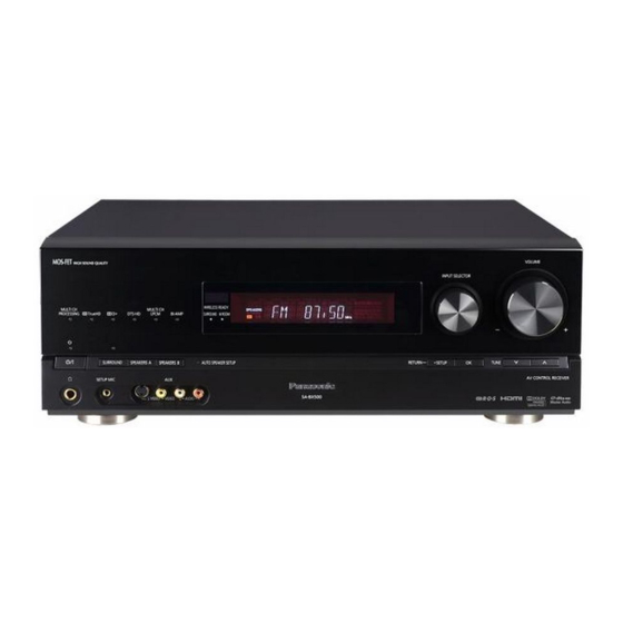
Main unit SA-BX500PP
GENERAL
Power supply:
Power consumption:
Power consumption in standby mode:
Power consumption in HDMI off mode:
Dimensions (W×H×D):
Mass:
Operating temperature range:
Operating humidity range:
AMPLIFIER SECTION
Rated minimum sine wave RMS power output
20 Hz-20 kHz both channels
driven (with AES17 filter)
0.7 % total harmonic distortion
Total harmonic distortion
AC 120V, 60 Hz
150 W
approx. 0.7 W
approx. 0.4 W
430 mm × 158.5 mm × 339
mm
(16-15/16" x 6-1/4" x 13-11/32")
Approx. 5 kg (11 lb.)
0 °C to 40 °C
20% to 80% RH
(no condensation)
130 W per channel (6 Ω)
AV Control Receiver
SA-BX500PP
Colour
(K).......................Black Type
Rated power at 20 Hz-20 kHz
Power output each channel driven at 20 Hz-20 kHz
(with AES17 filter)
Front (L/R):
Center:
Surround (L/R):
Surround Back (L/R):
Total Harmonic distortion:
Load impedance
Front (L/R)
A or B:
A and B:
BI-WIRE:
© 2008 Matsushita Electric Industrial Co. Ltd.. All
rights
reserved.
distribution is a violation of law.
ORDER NO. MD0808003CE
0.7% (6 Ω)
130 W per channel (6 Ω)
130 W per channel (6 Ω)
130 W per channel (6 Ω)
130 W per channel (6 Ω)
0.7% W
4 to 8 Ω
6 to 8 Ω
Unauthorized
copying
and
A1
Advertisement
Table of Contents

Related Manuals for Panasonic SA-BX500PP


Summary of Contents for Panasonic SA-BX500PP
-
Page 1: Specifications
ORDER NO. MD0808003CE AV Control Receiver SA-BX500PP Colour (K).......Black Type Specifications Main unit SA-BX500PP Rated power at 20 Hz-20 kHz 0.7% (6 Ω) GENERAL Power supply: AC 120V, 60 Hz Power output each channel driven at 20 Hz-20 kHz Power consumption:... - Page 2 SA-BX500PP 4 to 8 Ω An exclusive terminal for SH-PD10 (option) Center: 6 to 8 Ω VIDEO SECTION Surround (L/R): Output voltage at 1 V input (unbalanced) 6 to 8 Ω 1 ± 0.1 Vp-p Surround Back (L/R): Maximum input voltage 6 to 8 Ω...
-
Page 3: Table Of Contents
SA-BX500PP CONTENTS Page Page 1 Safety Precautions 7.14. Disassembly and checking of D-Amp A (4CH) P.C.B. 1.1. GENERAL GUIDELINES 7.15. Replacement of Digital Amp IC (IC5000) of D-Amp A 1.2. Before Repair and Adjustment (4CH) P.C.B. 1.3. Protection Circuitry 7.16. Disassembly and checking of HDMI side (A) and side (B) 1.4. - Page 4 SA-BX500PP 13 Schematic Diagram 14.4. D-Port, Panel, S-Video P.C.B. 13.1. HDMI Circuit 14.5. Headphone, Speaker, Digital, Video, Volume P.C.B. 13.2. DSP Circuit 14.6. Wireless Adapter, Fan, AC Inlet P.C.B. 13.3. Main Circuit 14.7. D-Amp A (4CH) P.C.B. 13.4. Panel Circuit 14.8.
-
Page 5: Safety Precautions
SA-BX500PP 1 Safety Precautions 1.1. GENERAL GUIDELINES 1. When servicing, observe the original lead dress. If a short circuit is found, replace all parts which have been overheated or damaged by the short circuit. 2. After servicing, see to it that all the protective devices such as insulation barriers, insulation papers shields are properly installed. -
Page 6: Safety Parts Information
SA-BX500PP “shorted”, or if speaker systems with an impedance less than the indicated rated impedance of the amplifier are used. If this occurs, follow the procedure outlines below: 1. Turn off the power. 2. Determine the cause of the problem and correct it. -
Page 7: Prevention Of Electrostatic Discharge (Esd) To
SA-BX500PP 2 Prevention of Electrostatic Discharge (ESD) to Electrostatically Sensitive (ES) Devices Some semiconductor (solid state) devices can be damaged easily by static electricity. Such components commonly are called Electrostatically Sensitive (ES) Devices. Examples of typical ES devices are integrated circuits and some field-effect transistors and semiconductor “chip”... -
Page 8: About Lead Free Solder (Pbf)
SA-BX500PP 3 About Lead Free Solder (PbF) 3.1. Service caution based on legal restrictions 3.1.1. General description about Lead Free Solder (PbF) The lead free solder has been used in the mounting process of all electrical components on the printed circuit boards used for this equipment in considering the globally environmental conservation. -
Page 9: Accessories
SA-BX500PP 4 Accessories • • • • Note: Refer to “Replacement Parts List” (Section 25) for the part number. AM loop antenna Remote control AC cord Setup microphone Front terminal cover FM indoor antenna... -
Page 10: Operation Procedures
SA-BX500PP 5 Operation Procedures 5.1. Remote Control Key Buttons Operations Remote control For switching an input Batteries source on and off/ Source switching/ Press on the tab to open. Switching remote control modes SYSTEM RECORDER Power button INPUT SELECTOR FM/AM... -
Page 11: Main Unit Key Buttons Operations
SA-BX500PP 5.2. Main Unit Key Buttons Operations This unit Lights on when BI-AMP is on Lights on when playing a disc using multi-channel LPCM format For switching the surround playback on Lights on when playing a disc using and off (The indicator lights up when the high definition audio format such as surround playback is on.) -
Page 12: Using The Viera Link "Hdavi Control
HDMI CEC cannot be guaranteed. This unit suppor ts "HDAVI Control 1" function. This standard is compatible with Panasonic’s conventional HDAVI equipment. Please refer to individual manuals for other manufacturers’ equipment supporting VIERA Link function. What you can do with VIERA Link "HDAVI Control"... -
Page 13: Main Unit Connections
SA-BX500PP 5.4. Main Unit Connections 5.4.1. Video & Audio Terminals Basic connections Connecting cables to video and audio terminals (Connecting equipment without HDMI terminal) Connection cab Video cable Audio cable Video connection cable (not included) Optical fiber cable (not included) -
Page 14: Basic Connections
RP-CDHG50 (5.0 m/16.4 ft), etc. HDMI cable notes It is recommended that you use Panasonic s HDMI cable. This unit incorporates HDMI (V .1.3 with Deep Color) technology. Please use High Speed HDMI Cables that have the HDMI logo (as shown on the cover). - Page 15 SA-BX500PP 5.4.3. S Video and audio Terminals Connecting cables to S video and audio terminals Connection cable Video cable S VIDEO connection cab le (not included) Audio cable Optical fibre cable (not included) Stereo connection cable (not included) White (L)
- Page 16 SA-BX500PP 5.4.4. Component and audio terminals Connecting cables to component and audio terminals The component video terminals can produce more accurate colours than the S video terminals. Connection cable Video cable Audio cable Video connection cable (not included) Optical fibre cable (not included)
-
Page 17: Other Connections
SA-BX500PP 5.4.5. Other connections Other connections Connection cable Video cable Video connection cable (not included) S VIDEO connection cab le (not included) Audio cable Coaxial cable (not included) Stereo phono cab le (not included) White (L) To enjoy analogue sounds... - Page 18 SA-BX500PP Other connections To connect the unit for audio or picture recording You can record audio or pictures to the equipment connected to DVD recorder output terminal (AUDIO, VIDEO, S VIDEO). Rear panel BACK (DVD RECORDER) (BD/DVD PLAYER) (CABLE/SAT) HDMI 2...
- Page 19 SA-BX500PP 5.4.6. For speakers Connecting other speakers To connect bi-wire speakers Make sure to select YES in Making bi-wire setting when you connect the unit to bi-wire speakers. The speakers do not produce adequate sounds unless you make this setting.
-
Page 20: Connecting Antennas
SA-BX500PP To enjoy wireless audio with SH-FX67 You can connect left and right surround speakers wirelessly by using Panasonic SH-FX67 (a set consisted of a digital transmitter and a wireless system sold separately) with the unit. To use these options, insert the digital transmitter into the unit s digital transmitter terminal and connect surround speakers to SH-FX67’s wireless system. -
Page 21: Self-Diagnosis And Display Function
SA-BX500PP 6 Self-Diagnosis and Display Function This unit is equipped with the self diagnosis display function, which alarms faulty operation with error code. Use this function during servicing. 6.1. Automatically Displayed Error Codes An error code automatically appears on the display (FL Display) when faulty operation is detected. Refer to Fig. 6.1. -
Page 22: Overload/Shutdown Detection Internal Condition
SA-BX500PP Message Cause/countermeasure NO LS/RS SPEAKERS Surround speakers are set as absent. Change their setting to present. LS/RS SBL/SBR Surround and surround back speakers are set as SPEAKERS absent. Change their setting to present. NO SBL/SBR SPEAKERS Surround back speakers are set as absent. -
Page 23: Returning To Normal Display
SA-BX500PP Fig 6.2 3. When the [SPEAKER A] button is pressed, the current program filing number [M45_XXXX] appears. The XXXX digit indicates the ROM checksum used for ROM collection, and if the unit is not loaded with ROM, “NO” appears. -
Page 24: Wireless Link
SA-BX500PP Fig 6.3 3. Doctor mode function at some remote control codes as below table. Remote Control Test Mode Function and settings Selector Surround Other settings Vol/Tone CH 1 TUNER Frequency: FM min. -48dB/0dB CH 2 TUNER Frequency: FM max. - Page 25 SA-BX500PP is not function. (Volume adjustment or Mute also unfunction) <FX67 Common frequency fixed method> Preparation: Beforehand, press remote control [FM/AM], remote control side, will appear FM/AM code stage. Below is operation of wireless frequency fixed method. Function Button Condition...
-
Page 26: Assembling And Disassembling
SA-BX500PP 7 Assembling and Disassembling “ATTENTION SERVICER” Be careful when disassembling and servicing. Some chassis components may have sharp edges. Special Note: 1. This section describes the disassembly procedures for all the major printed circuit boards and main components. 2. Before the disassembly process was carried out, do take special note that all safety precautions are to be carried out. -
Page 27: Disassembly Flow Chart
SA-BX500PP 7.1. Disassembly Flow Chart 7.3. Top Cabinet 7.4. DSP (Side A/B) 7.5. Speaker P.C.B. 716. HDMI (A/B) P.C.B. 7.20. Front Panel P.C.B. 7.6. D-Amp B (3CH) 7.17. S-Video & Video 7.21. Panel, Headphone & P.C.B. P.C.B. Volume P.C.B. 7.18. Wireless Adapter, Digital &... -
Page 28: Main Components And P.c.b. Locations
SA-BX500PP 7.2. Main Components and P.C.B. Locations... -
Page 29: Disassembly Of Top Cabinet
SA-BX500PP 7.3. Disassembly of Top Cabinet Step 1 Remove 4 screws at the sides of the top cabinet. Step 2 Remove 5 screws at the rear of the top cabinet. Step 3 Lift up the top cabinet as arrow shown. -
Page 30: Disassembly And Checking Of Speaker P.c.b
SA-BX500PP Step 4 Flip the DSP P.C.B. as arrow shown. Step 3 Proceed to check the Speaker P.C.B. Step 5 Proceed to check Side B of DSP P.C.B.. Caution: Insulate Speaker P.C.B. from other parts by insulating material (e.g.: plastic). - Page 31 SA-BX500PP Step 8 Remove 2 P.C.B. bracket on D-Amp B (3CH) P.C.B. Step 9 Flip D-Amp B (3CH) and Fan P.C.B. as arrow shown. Step 4 Cut 3 tie wraps. Step 10 Move Speaker P.C.B. as arrow shown. Note: During assembling it is necessary to use tie wraps.
-
Page 32: Replacement Of Digital Amp Ic (Ic5000) Of D-Amp B
SA-BX500PP P.C.B. Step 4 Remove the D-Amp B (3CH) P.C.B. as arrow shown. Caution: Insulate Speaker P.C.B. from other parts insulating Step 5 Desolder pins of the digital amp IC (IC5000) on the back material (e.g.: plastic). side of D-Amp P.C.B. -
Page 33: Disassembly And Checking Of Smps & Ac Inlet
SA-BX500PP Step 6 Move up the support bar as arrow shown and beware of the catches. Special Note: For replacement of IC5200, IC5300, repeat the (Step 1) to (Step 8). Refer to the diagrams of D-Amp B (3CH) P.C.B. (Item 14.8) for location of the parts. -
Page 34: Replacement Of Switch Regulator Ic (Ic5701)
SA-BX500PP Step 8 Connect extension cable REXX0651 (8P cable from Special Note: During reassembling procedures, ensure the H5801 to CN5500). P.C.B. is seated properly at the locators. Step 9 Remove AC Inlet shield plate unit. Step 10 Remove P.C.B. bracket. -
Page 35: Replacement Of Switch Regulator Diode (D5702)
SA-BX500PP Step 3 Solder pins of the switch regulator IC (IC5701) on the Step 2 Remove 1 screw from the switch regulator IC (IC5701). reverse side of SMPS P.C.B. Step 3 Remove the switch regulator IC (IC5701) from the heatsink unit B. - Page 36 SA-BX500PP heatsink unit B. Special Note: Ensure the switch regulator diode (D5702) is tightly screwed to the heatsink unit B. Step 3 Fix the heatsink unit B on SMPS P.C.B. in the direction of arrows. Step 4 Fix and screw the switch regulator IC (IC5701) to the heatsink unit B Step 3 Remove 1 screw from the switch regulator IC (IC5701).
-
Page 37: Replacement Of Regulator Diode (D5801)
SA-BX500PP screwed to the heatsink unit C. 7.11. Replacement of Regulator Diode (D5801) • • • • Follow (Step 1) to (Step 4) of Item 7.3. • • • • Follow (Step 1) to (Step 3) of Item 7.5. • • • • Follow (Step 1) to (Step 10) of Item 7.6. -
Page 38: Replacement Of Regulator Diode (D5803)
SA-BX500PP Step 2 Remove 1 screw from the regulator diode (D5802). Step 3 Remove the regulator diode (D5802) from the heatsink unit C. Step 3 Solder pins of the regulator diode (D5802) on the reverse side of SMPS P.C.B. Caution: Handle the heatsink unit C with caution due to its high temperature after prolonged use. -
Page 39: Disassembly And Checking Of D-Amp A (4Ch) P.c.b
SA-BX500PP Step 2 Remove 1 screw from the regulator diode (D5803). Step 3 Solder pins of the regulator diode (D5803) on the Step 3 Remove the regulator diode (D5803) from the heatsink reverse side of SMPS P.C.B. unit C. Caution: Handle the heatsink unit C with caution due to its high temperature after prolonged use. -
Page 40: Replacement Of Digital Amp Ic (Ic5000) Of D-Amp A
SA-BX500PP Caution: Lay an Insulated material to support the D-Amp A (4CH) P.C.B. Step 2 Remove 2 screws on D-Amp (4CH) P.C.B.. Step 3 Attach original cable with extension cable REXX0651 (8P cable from H5801 to CN5500). Step 4 Connect extension cable REEX0815 (17P cable from CN2802 to CN5050). -
Page 41: Disassembly And Checking Of Hdmi Side (A) And Side (B)
SA-BX500PP (CN5501) on D-Amp A (4CH) P.C.B. injuries. Step 4 Detach 12P cable at the connector (JW4602) on Speaker P.C.B. Step 5 Remove the D-Amp A (4CH) P.C.B. as arrow shown. Special Note: For replacement of IC5200, IC5300 & IC5400, repeat the (Step 1) to (Step 8). -
Page 42: Disassembly And Checking Of S-Video & Video P.c.b
SA-BX500PP Step 3 Proceed to check S-Video and Video P.C.B.. Step 4 Proceed to check side (B) of HDMI P.C.B. 7.17. Disassembly and Checking of S-Video & Video P.C.B. • • • • Follow (Step 1) to (Step 4) of Item 7.3. - Page 43 SA-BX500PP Step 3 Remove 7 screws on the rear panel. Step 9 Detach 11P FFC cable at the connector (PB4401) on Digital P.C.B. Step 10 Remove Digital P.C.B. as arrow shown. Step 4 Release 2 catches at the rear panel.
-
Page 44: Disassembly And Checking Of Main (Side A/B) P.c.b
SA-BX500PP Step 4 Position the P.C.B as diagram show. Step 5 Connect Wireless Adapter, Digital & D-Port P.C.B.. Step 12 Position D-Port P.C.B. as Diagram shown. Step 6 Proceed to check Side A of Main P.C.B. Step 13 Connect 22P FFC Cable at the connector (CN6301) on Wireless Adapter P.C.B.. -
Page 45: Disassembly Of Front Panel
SA-BX500PP Step 3 Detach 30P FFC cable at the connector (PB501) on Main P.C.B.. Step 4 Detach 7P cable at the connector (PB502) on Main P.C.B. Step 5 Detach 5P cable at the connector (PB1002) on Main P.C.B. Step 10 Proceed to check Side B of Main P.C.B. -
Page 46: Disassembly And Checking Of Panel, Headphone, Volume
SA-BX500PP Step 8 Remove 4 screws. Step 3 Remove 6 screws at front panel shield plate. Step 9 Slightly move up 2 support bars and DSP P.C.B. to Step 4 Remove the front panel shield plate. release the catches. Step 10 Release 2 tabs. - Page 47 SA-BX500PP Caution: Keep the VCR Earth Angle in safe place. Avoid denting it. Place it back during assembling. Step 8 Connect Panel, Volume, Headphone P.C.B. Step 9 Proceed to check Panel, Volume, Headphone P.C.B.
-
Page 48: Voltage And Waveform Chart
SA-BX500PP 8 Voltage and Waveform Chart 8.1. HDMI P.C.B. REF NO. IC2001 MODE CD PLAY STANDBY IC2002 REF NO. MODE CD PLAY STANDBY IC2002 REF NO. MODE CD PLAY STANDBY REF NO. IC2002 MODE CD PLAY STANDBY REF NO. IC2002... - Page 49 STANDBY Q2231 Q2232 Q2233 REF NO. MODE CD PLAY -0.2 STANDBY -0.2 REF NO. Q2234 Q2235 Q2236 MODE CD PLAY -0.2 -0.2 -0.2 STANDBY -0.2 -0.2 -0.2 QR2001 QR2002 QR2231 QR2232 REF NO. MODE CD PLAY STANDBY SA-BX500PP HDMI P.C.B.
-
Page 50: Dsp P.c.b
SA-BX500PP 8.2. DSP P.C.B. REF NO. IC3001 MODE CD PLAY STANDBY IC3001 REF NO. MODE CD PLAY STANDBY IC3001 REF NO. MODE CD PLAY STANDBY REF NO. IC3001 MODE CD PLAY STANDBY IC3001 REF NO. MODE CD PLAY STANDBY IC3001 REF NO. - Page 51 SA-BX500PP IC3101 REF NO. MODE CD PLAY STANDBY REF NO. IC3101 MODE CD PLAY STANDBY IC3101 REF NO. MODE CD PLAY STANDBY REF NO. IC3101 MODE CD PLAY STANDBY REF NO. IC3101 MODE CD PLAY STANDBY IC3101 REF NO. MODE...
- Page 52 STANDBY REF NO. IC3551 MODE CD PLAY STANDBY REF NO. IC3601 MODE CD PLAY STANDBY IC3602 REF NO. MODE CD PLAY STANDBY Q3601 REF NO. MODE CD PLAY STANDBY REF NO. QR3401 QR3601 MODE CD PLAY STANDBY SA-BX500PP DSP P.C.B.
-
Page 53: D-Amp A (4Ch) P.c.b
REF NO. IC5500 MODE CD PLAY STANDBY REF NO. IC5501 MODE CD PLAY STANDBY REF NO. Q5101 Q5102 Q5601 Q5602 Q5603 MODE CD PLAY STANDBY REF NO. Q5604 Q5640 Q5641 Q5642 Q5644 MODE CD PLAY STANDBY SA-BX500PP D-AMP A (4CH) P.C.B. -
Page 54: D-Amp B (3Ch) P.c.b
REF NO. IC5500 MODE CD PLAY STANDBY REF NO. IC5501 MODE CD PLAY STANDBY REF NO. Q5101 Q5102 Q5601 Q5602 Q5603 MODE CD PLAY STANDBY Q5604 Q5640 Q5642 Q5644 REF NO. MODE CD PLAY STANDBY SA-BX500PP D-AMP B (3CH) P.C.B. -
Page 55: Main P.c.b
SA-BX500PP 8.5. Main P.C.B. REF NO. IC101 MODE CD PLAY STANDBY IC1001 REF NO. MODE CD PLAY STANDBY REF NO. IC1102 MODE CD PLAY -7.5 STANDBY -7.5 IC4001 REF NO. MODE CD PLAY -7.5 STANDBY -7.5 REF NO. IC4001 MODE... - Page 56 SA-BX500PP REF NO. IC4261 MODE CD PLAY STANDBY REF NO. IC4301 MODE CD PLAY -7.6 STANDBY -7.6 IC4303 REF NO. MODE CD PLAY -6.2 -7.6 -6.2 STANDBY -6.2 -7.6 -6.2 REF NO. IC4304 MODE CD PLAY -6.2 -7.6 -6.2 STANDBY -6.2...
- Page 57 CD PLAY -7.2 -7.2 -7.2 STANDBY -7.2 -7.2 -7.2 QR4306 QR4401 QR4402 QR4403 QR7001 REF NO. MODE CD PLAY STANDBY QR7105 QR7106 QR7109 QR8011 QR8012 REF NO. MODE CD PLAY STANDBY QR8017 REF NO. MODE CD PLAY STANDBY SA-BX500PP MAIN P.C.B.
-
Page 58: Panel P.c.b
QR508 QR509 QR510 MODE CD PLAY STANDBY QR511 QR512 QR513 REF NO. MODE CD PLAY STANDBY SA-BX500PP PANEL P.C.B. 8.7. Digital, Speaker & Fan P.C.B. IC4401 REF NO. MODE CD PLAY STANDBY SA-BX500PP DIGITAL P.C.B. Q4601 Q4602 Q4603 Q4604 REF NO. -
Page 59: Video P.c.b
CD PLAY STANDBY Q1001 Q1002 Q1003 REF NO. MODE CD PLAY -4.9 -7.5 -5.5 STANDBY -4.9 -7.5 -5.5 SA-BX500PP VIDEO P.C.B. 8.9. S-Video P.C.B. REF NO. IC1051 MODE CD PLAY -4.9 STANDBY -4.9 REF NO. IC1052 MODE CD PLAY -4.9 STANDBY -4.9... -
Page 60: Waveform Chart
SA-BX500PP 8.11. Waveform Chart 8.11.1. Waveform 1 1.5Vp-p(2usec/div) 2.6Vp-p(20usec/div) 1.0Vp-p(20usec/div) 0.9Vp-p(2msec/div) 6Vp-p(500nsec/div) 4Vp-p(1usec/div) 3.4Vp-p(500nsec/div) 3.4Vp-p(500nsec/div) 5.6Vp-p(1usec/div) 0.3Vp-p(200usec/div) 3Vp-p(200usec/div) 5.6Vp-p(200usec/div) 5.6Vp-p(1usec/div) 0.84Vp-p(200usec/div) 80Vp-p(1usec/div) 0.84Vp-p(200usec/div) 0.84Vp-p(200usec/div) 80Vp-p(1usec/div) 0.84Vp-p(200usec/div) 5.6Vp-p(1usec/div) 0.84Vp-p(200usec/div) 0.84Vp-p(200usec/div) 80Vp-p(1usec/div) 5.6Vp-p(1usec/div) - Page 61 SA-BX500PP 8.11.2. Waveform 2 0.84Vp-p(200usec/div) 80Vp-p(1usec/div) 0.84Vp-p(200usec/div) 7.2Vp-p(500nsec/div) 5.6Vp-p(500usec/div) 400Vp-p(2usec/div) 2Vp-p(5usec/div) 2Vp-p(5usec/div) 240Vp-p(50usec/div) 9.6Vp-p(5usec/div)
-
Page 62: Illustration Of Ic's, Transistors And Diodes
SA-BX500PP 9 Illustration of IC’s, Transistors and Diodes C0JBAB000685 C2CBJH000147 (100p) C0ABBB000189 (8p) C0FBAK000026 (16p) C1AB00001486 C0JBAZ002811 (20p) C0DBZYY00018 (8p) C1AB00001931 (16p) C1AB00002951 C0ABBB000038 (8p) C0JBAZ001466 (20p) C0DBZYE00002 (8p) C1AB00002029 (24p) No.1 C0DBAKG00007 (8p) C0JBAZ002843 (30p) C0JBAB000902 (14p) C0FBBK000044 (30p) -
Page 63: Wiring Connection Diagram
SURROUND 8CH) PB3002 BACK VIDEO P.C.B. HDMI 1 IN SUBWOOFER/ (SOLDER SIDE) (DVD RECORDER) PB2004 CN3005 CENTER PB3005 PA1001 JWA1501* PA1002 CN2004 JK2101 PB603 (CD) IN CN8004 CN8003 JK4001 HDMI OUT CN3001 CN2003 * FOR INDICATION ONLY SA-BX500PP WIRING CONNECTION... - Page 64 SA-BX500PP...
-
Page 65: Block Diagram
VIDEO (COMPOSITE VIDEO) QR8011,QR8012 HDMIMUTE DIS nHDMI MUTE TO AUDIO CN3005 PB3005 SPI DI SPIDI CN3005 PB3005 SYNC SPIDO FROM/TO CN3005 PB3005 SPICLK SPICLK PB2004 CN2004 CN3005 PB3005 HDMI MUTE FSHIFT HDMI MUTE FROM HDMI FSHIFT SA-BX500PP SYSTEM CONTROL BLOCK DIAGRAM... -
Page 66: Hdmi
Q2232 LEVEL SWITCHING SHIFTER TO DSP Q2235 I2S 1 D CN2003 CN3001 LEVEL SHIFTER Q2233 Q2234 I2S 2 D CN2003 CN3001 LEVEL SWITCHING SHIFTER Q2236 LEVEL I2S 3 D CN2003 CN3001 SHIFTER IEC958 D CN2003 CN3001 SA-BX500PP HDMI BLOCK DIAGRAM... -
Page 67: Ic Terminal (Hdmi) Chart
IC2201 / HDMI RECEIVER SIGNAL NAME Port Name Pin No Pin No Port Name TMDS D0- R2X0- R2X0- TMDS D0+ R2X0+ R2X0+ TMDS D1- R2X1- R2X1- TMDS D1+ R2X1+ R2X1+ TMDS D2- R2X2- R2X2- TMDS D2+ R2X2+ R2X2+ SA-BX500PP IC TERMINAL (HDMI) CHART... -
Page 68: Dsp
34 CKE PB3005 CN3005 DAZFLAG DAC DZF DAZFLAG DZF2 DZFR 17 RAS DZF1 DZFL 16 CAS PB3005 CN3005 DACE DAC CS DACE 18 CS 14 LDQM 36 UDQM CN3005 PB3005 FROM DAC RST SYSTEM CONTROL SA-BX500PP DSP (SECTION 1/2) BLOCK DIAGRAM... - Page 69 SDRAM DSP1 TDI CN8002 CN8005 CN3006 JTAG TMS PB3002 CN3002 LOUT4 TC - 6 A1_2 - A10_2, A17_2 A0 - A9, BA PB3002 CN3002 ROUT4 TC - 7 D16_2 - D31_2 D0 - D15 SA-BX500PP DSP (SECTION 2/2) BLOCK DIAGRAM...
-
Page 70: Ic Terminal (Dsp) Chart
DATA18 D19_1 DATA19 D20_1 DATA20 D21_1 DATA21 D22_1 DATA22 D23_1 DATA23 D24_1 DATA24 D25_1 DATA25 D26_1 DATA26 DQ10 D27_1 DATA27 DQ11 D28_1 DATA28 DQ12 D29_1 DATA29 DQ13 D30_1 DATA30 DQ14 D31_1 DATA31 DQ15 SA-BX500PP IC TERMINAL (DSP) (SECTION 1/2) CHART... - Page 71 DATA18 D19_2 DATA19 D20_2 DATA20 D21_2 DATA21 D22_2 DATA22 D23_2 DATA23 D24_2 DATA24 D25_2 DATA25 D26_2 DATA26 DQ10 D27_2 DATA27 DQ11 D28_2 DATA28 DQ12 D29_2 DATA29 DQ13 D30_2 DATA30 DQ14 D31_2 DATA31 DQ15 SA-BX500PP IC TERMINAL (DSP) (SECTION 2/2) CHART...
-
Page 72: Audio
SETUP MIC PC501 PB1002 A+7.5V DGND QR4012 VOL DA Q4008 VOL DA MUTING MIC MUTE MUTING FROM CONTROL SYSTEM CONTROL VOL CL BK+3.3V VOL CL FROM SYSTEM CONTROL QR4009 MUTING +6DB CONTROL SECTION (2/2) BK+3.3V SA-BX500PP AUDIO (SECTION 1/2) BLOCK DIAGRAM... - Page 73 CONTROL CONTROL QR4306 IC4261 C0ABBB000038 BK+3.3V BK+3.3V MUTING nHDMI MUTE nHDMI MUTE OP-AMP(SURR. OUT 2CH) CONTROL SOUT L PB3002 CN3002 SOUT 2CHL SOUT 2CHL TO DSP SOUT R SOUT 2CHR SOUT 2CHR PB3002 CN3002 SA-BX500PP AUDIO (SECTION 2/2) BLOCK DIAGRAM...
-
Page 74: Digital Audio Amp (4Ch)
DC DET Q5640, Q5642, Q5644 CN5501 JW5993 CN5991 FAN DC OUT H5801 CN5500 FAN MOTOR FAN DC FROM POWER DRIVE CN5501 JW5993 CN5991 FAN GND DIGITAL AUDIO OSC2 CN8003 CN5050 OSC2 AMP (3CH) SA-BX500PP DIGITAL AUDIO AMP (4CH) BLOCK DIAGRAM... -
Page 75: Digital Audio Amp (3Ch)
CN5050 DC DET DC DETECT FROM DIGITAL AUDIO OSC2 CN8004 CN5050 OSC2 AMP (4CH) Q5640, Q5642, Q5644 FAN DC OUT CN5501 H5802 CN5500 FAN DC FAN MOTOR FROM POWER DRIVE FAN GND CN5501 SA-BX500PP DIGITAL AUDIO AMP (3CH) BLOCK DIAGRAM... -
Page 76: Speaker Channel
JK4603 FRONT B (HF) R JK4603 CN5550 JW4602 SBR- FROM CN5550 JW4602 SBL- SBL- RY4604 DIGITAL AUDIO AMP (4CH) JK4603 FRONT A (LF) L JK4603 JK4603 CN5550 JW4602 FRONT A (LF) R JK4603 CN5550 JW4602 SA-BX500PP SPEAKER CHANNEL BLOCK DIAGRAM... -
Page 77: Video (Component & Composite Video)
V SEL JK1002 (BD/DVD PLAYER) 75Ohm JK1002 DRIVER JK1001 (MONITOR) (DVD RECORDER) 75Ohm JK1001 DRIVER (VCR) (DVD RECORDER) JK1003 IC1003 75Ohm DRIVER C1AB00001486 VIDEO SWITCH (GAME) BUF. (CABLE/SAT) JK503 PC501 PA1002 (VIDEO) PANEL P.C.B. SA-BX500PP VIDEO (COMPONENT/COMPOSITE VIDEO) BLOCK DIAGRAM... -
Page 78: Video (S-Video)
MON OUT C REC IN C AUX S-VIDEO C 75Ohm DRIVER PC501 PA1051 AUX S-VIDEO Y VCR IN C REC OUT C JK501 (S-VIDEO) C IN 75Ohm PC501 PA1051 AUX S-VIDEO C DRIVER PANEL P.C.B. SA-BX500PP VIDEO (S-VIDEO) BLOCK DIAGRAM... -
Page 79: Power
POWER CONTROL Q7004 D5804 CN5802 CN7001 A-7.5V A-7.5V - 13V A-7.5V REGULATOR IC5801 C0DABFC00002 SHUNT REGULATOR Q5802, D5806 Q5803 PC5720 FROM AMBP CN5802 CN7001 SWITCHING FEED BACK FEED BACK CIRCUIT SYSTEM CONTROL SECTION (2/2) SA-BX500PP POWER (SECTION 1/2) BLOCK DIAGRAM... - Page 80 VIDEO P.C.B. S-VIDEO P.C.B. Q1001 A+7.5V PB1001 PA1001 REGULATOR QR4014 ADJUST JWA1501 JWB1501 Q1003 CONTROL DCDET PB1001 PA1001 DCDET IC4050 DETECT C0ABBB000038 JWA1501 JWB1501 OP-AMP(BUFFER) Q1002 VOUT PB1001 PA1001 A-7.5V REGULATOR Q69831 POWER -VCC SUPPLY SA-BX500PP POWER (SECTION 2/2) BLOCK DIAGRAM...
-
Page 81: Schematic Diagram Notes
SA-BX500PP : Mic signal line 12 Schematic Diagram Notes • • • • This schematic diagram may be modified at any time with the development of new technology. Notes: S501: Power switch ( S502: Speaker A switch. S503: Surround switch. - Page 82 SA-BX500PP...
-
Page 83: Schematic Diagram
Q2105 B1ABCF000079 C2102 B1ABCF000079 DIODE 330P R2059 C2124 BUFFER R2108 R2060 Q2102 100K CEC_OUT LB2105 - LB2108 B1ABCF000079 LB2109 R2061 J0JHC0000021 J0JHC0000021 SWITCHING LB2110 Q2104 J0JHC0000021 B1ABCF000079 BUFFER BK5V TO HDMI SECTION (2/4) SA-BX500PP HDMI CIRCUIT TO HDMI SECTION (3/4) - Page 84 SA-BX500PP SCHEMATIC DIAGRAM - 2 HDMI CIRCUIT : +B SIGNAL LINE : MAIN SIGNAL LINE : VIDEO SIGNAL LINE : AUDIO SIGNAL LINE CN2004 QR2002 R2041 B1GBCFJJ0007 CEC_LED R2035 CN2003 CEC_LED DC DETECT D2001 MA2J72800L H_LED R2057 R2036 MCLK_BACK HDMI_LED...
- Page 85 VA2214 VA2218 D0 GND R0PWR5V TMDS D0+ DSCL0 TMDS D1- DSDA0 VA2215 VA2219 TO HDMI D1 GND SECTION (4/4) TMDS D1+ D2201 B0ACCK000005 TMDS D2- VA2216 VA2220 D2202 B0ACCK000005 D2 GND TMDS D2+ VA2213 - VA2220 EZAEG2A50AX SA-BX500PP HDMI CIRCUIT...
- Page 86 SA-BX500PP SCHEMATIC DIAGRAM - 4 HDMI CIRCUIT : +B SIGNAL LINE : MAIN SIGNAL LINE : VIDEO SIGNAL LINE : AUDIO SIGNAL LINE IC2233 R2231 TO HDMI C0CBCAG00015 SECTION (2/4) +1.8V REGULATOR HDMI POWER LB2231 LB2235 BK2.5V HOT PLUG J0JHC0000021...
-
Page 87: Dsp Circuit
A2_1 R3021 ADDR2 A0_1 R3022 R3080 D30_1 ADDR0 DATA30 C3015 R3081 D31_1 VDDEXT DATA31 R3082 D29_1 C3004 C3060 C3017 C3025 C3026 C3030 C3033 C3034 C3040 C3041 C3045 C3048 LB3002 J0JGC0000020 C3091 1000P TO DSP SECTION (4/6) GND1 SA-BX500PP DSP CIRCUIT... - Page 88 A0_2 R3122 C3157 R3175 D30_2 ADDR0 DATA30 R3176 D31_2 VDDEXT DATA31 C3115 R3177 D29_2 TO DSP SECTION (3/6) C3104 C3160 C3117 C3125 C3126 C3130 C3133 C3134 C3140 C3141 C3145 C3119 C3148 SA-BX500PP DSP CIRCUIT C3191 TO DSP SECTION (5/6) GND2...
- Page 89 R3754 DC_DET DGND R3755 OPT IN DGND CN3004 DGND DGND R3731 DGND R3732 DIGITAL CIRCUIT DGND R3733 (PB4401) IN SCHEMATIC DGND R3734 DIAGRAM - 24 DGND R3735 D3.3V D3.3V SA-BX500PP DSP CIRCUIT TO DSP SECTION (6/6) TO DSP SECTION (2/6)
- Page 90 SECTION (5/6) D3603 QR3601 MAZ802400L B1GBCFJJ0001 L3602 LB3602 DC DETECT G1A220G00006 J0JHC0000032 D1.2V R3603 0.047 LB3601 C3616 6.3V1000 J0JHC0000032 V5/PWON VREF/SS R3602 C3604 IC3601 C0DBAKG00007 DC-DC CONVERTER IC3602 C0DBZYY00018 D+3.3V REGULATOR D3602 B0ECKM000016 D3.3V R3601 C3611 470P CONT SA-BX500PP DSP CIRCUIT...
- Page 91 DIGITAL AUDIO LB3408 NC(AVSS) COUT TRANSCEIVER J0JGC0000020 C3418 LB3401 BOUT J0JGC0000020 TEST1 [47] NC(AVSS) [13] TVDD [48] RX3 [14] NC(DVSS) R3407 C3426 IC3402 OUT_Y LB3407 C0JBAB000661 J0JGC0000020 IN_A INVERTER TO DSP R3403 C3433 SECTION (6/6) X3402 H0J245500091 SA-BX500PP DSP CIRCUIT...
- Page 92 DSP_TMS DSP_EMU DSP2_TDO C3506 0.01 AGND C3502 C3504 6.3V47 R3501 LB3501 J0JBC0000041 6.3V100 D3506 MA2J11100L DAC_DZF D3501 MA2J11100L C3501 C3503 IC3501 C0FBBK000044 D/A CONVERTER C3507 C3505 DGND C3508 16V22 R3507 LB3502 J0JBC0000041 TO DSP SECTION (5/6) R3902 SA-BX500PP DSP CIRCUIT...
-
Page 93: Main Circuit
SA-BX500PP 13.3. Main Circuit SCHEMATIC DIAGRAM - 11 MAIN(AUDIO) CIRCUIT : +B SIGNAL LINE : -B SIGNAL LINE : MAIN SIGNAL LINE : IPOD AUDIO SIGNAL LINE : AM/FM SIGNAL LINE : MIC SIGNAL LINE : AUDIO SIGNAL LINE JK4007... - Page 94 SA-BX500PP SCHEMATIC DIAGRAM - 12 MAIN(AUDIO) CIRCUIT : +B SIGNAL LINE : -B SIGNAL LINE : MAIN SIGNAL LINE : IPOD AUDIO SIGNAL LINE : AM/FM SIGNAL LINE : MIC SIGNAL LINE : AUDIO SIGNAL LINE BK+3R3V BK+3R3V IC4051 DSP_A+5V...
- Page 95 PB1002 2.2K MIC_OUT C4166 R4170 R4174 C4174 R4182 R4164 C4164 R4176 C4172 MIC_OUT 1.5K 330P 25V10 3.9K 1.5K 330P 25V10 3.9K PANEL CIRCUIT MIC_GND FVCR2IN_R (PC501*) FVCR2IN_R AGND AGND IN SCHEMATIC AGND DIAGRAM - 19 FVCR2IN_L FVCR2IN_L SA-BX500PP MAIN(AUDIO) CIRCUIT...
- Page 96 AU: MAIN(AUDIO): SCHEMATIC DIAGRAM 11 - 14 CP: MAIN(CPU): SCHEMATIC DIAGRAM 15 - 18 IC4014 IC4015 C0ABBB000125 C0ABBB000125 OP-AMP (SUBWOOFER OP-AMP (WIRELESS OUT/CENTER BUFFER) Q4014 FRONT BUFFER) B1GFGCAA0001 MUTING A+7R5V R4190 R4194 C4188 25V10 R4198 VOUT_SW 4.7K R4192 C4186 330P VOUT_FR SA-BX500PP MAIN(AUDIO) CIRCUIT...
- Page 97 C8047 4700P NPMUTE DGND JTAG_TDO MIC_MUTE MUTEF JTAG_EMU ADC_RST CLR# DAC_RST EXTIOSTB R8039 STB# SURR_LED EXTIOCL 100K SETUP_LED EXTIODO R8159 DATA D+5V 220K D+3R3V R8134 PWBPF C121 R8135 K8002 DGND QR8017 B1GBCFJJ0007 INVERTER SA-BX500PP MAIN(CPU) CIRCUIT TO MAIN(CPU) SECTION (3/4)
- Page 98 IPOD OUT DRIVE R1107 QR1102 AU: MAIN(AUDIO): SCHEMATIC DIAGRAM 11 - 14 B1GBCFJJ0007 CP: MAIN(CPU): SCHEMATIC DIAGRAM 15 - 18 IPOD IN CONTROL IC1001 QR1101 C0DBZYE00002 B1GBCFJJ0007 USB HIGH SPEED SWITCH IPOD OUT CONTROL SA-BX500PP MAIN(CPU) CIRCUIT TO MAIN(CPU) SECTION (4/4)
- Page 99 INVERTER AGND IC4405 VOUT_C.BUF IC4404 C0JBAS000008 WL_AGND C0ABBB000125 QUADRUPPLE ANALOG SWITCH OP-AMP (WIRELESS FRONT) QR4402 R4428 Q4404 B1GDCFNN0007 B1GFGCAA0001 INVERTER MUTING A+7.5V R4432 C4432 C4436 C4438 1000P 100P VOUT_FR.BUF WL_MR.SR R4442 C4440 WL_SROUT R4436 R4438 2.2K 25V10 SA-BX500PP MAIN(CPU) CIRCUIT...
- Page 100 SEL_ENC2 B1ADCF000001 LB8520 SEL ENC2 POWER CONTROL LB8521 J0JBC0000014 VOL_ENC1 C7052 VOL ENC1 1000P LB8522 J0JBC0000014 VOL_ENC2 VOL ENC2 SURR_LED LB8523 J0JBC0000014 SURROUND LED LB8524 J0JBC0000014 WL_MR_LED A-7.5V WL M.Room LED R8506 Q7004 DGND SA-BX500PP MAIN(CPU) CIRCUIT 2SB0621AHA A-7.5V REGULATOR...
-
Page 101: Panel Circuit
POWER LED CIRCUIT SYS6V MIC_GND (PB1002) AUX_R F_AUXIN_R IN SCHEMATIC AGND DIAGRAM - 13 AUX_L F_AUXIN_L VIDEO CIRCUIT VGND AUX_V (PA1002) F_AUX_VIDEO IN SCHEMATIC DIAGRAM - 23 F_S_Video_C SA-BX500PP PANEL CIRCUIT S-VIDEO CIRCUIT VGND (PA1051) F_S_Video_Y IN SCHEMATIC DIAGRAM - 21... - Page 102 VOL ENC1 LB523 C561 C560 VOL ENC2 100P 100P SURR_LED LB524 SURROUND LED WL_MR LB525 WL_M.Room LED DGND C563 JWA503* VOL ENC1 C562 16V10 VOL ENC2 VOLUME CIRCUIT (JWB503*) DGND KEY_GND IN SCHEMATIC KEY_GND DIAGRAM - 24 KEY2_ENT SA-BX500PP PANEL CIRCUIT...
-
Page 103: S-Video Circuit
D1051 MA2J11100L LB1058 R1078 C1082 J0JBC0000033 0.022 REC_OUT_C D1052 JK1052 MA2J11100L F_AUX_VIDEO_C C1078 LB1052 16V47 J0JBC0000033 PLA_IN_Y V_SEL (BD/DVD PLAYER) LB1051 C1070 J0JBC0000033 0.022 PLA_IN_C LB1054 R1072 J0JBC0000033 MON_OUT_Y SA-BX500PP S-VIDEO CIRCUIT (TV MONITOR) LB1053 R1071 C1081 J0JBC0000033 0.022 MON_OUT_C... -
Page 104: Speaker Circuit
RELAY CONTROL MAIN(CPU) 3.3K A_SP CIRCUIT B_SP (PB603) SP_RELAY_+B IN SCHEMATIC SPGND Q4602 DIAGRAM - 18 B1ABGC000001 R4602 RELAY CONTROL 3.3K L4609 G0B9R5K00003 D4602 B0ACCK000005 Q4604 B1ABGC000001 R4604 3.3K RELAY CONTROL Q4603 B1ABGC000001 R4603 3.3K RELAY CONTROL SA-BX500PP SPEAKER CIRCUIT... -
Page 105: Video Circuit
VIDEO AMP Q1002 DVR_PB PB (BLUE) 2SB0621AHA (DVD RECORDER) -5V REGULATOR C1013 DVR_Y DVR_PR PR (RED) C1017 R1014 STB_Y DVR_PB R1018 DVD_Y Y (GREEN) MON_Y STB_PB R1019 DVD_PB MON_PB PB (BLUE) (TV MONITOR) SA-BX500PP VIDEO CIRCUIT R1020 MON_PR PR (RED) -
Page 106: Fan Circuit
IN SCHEMATIC DGND R4401 FAN LOCK DETECT DIAGRAM - 7 RX1(COAX) R5991 C5991 OUTPUT DGND OPTICAL 2 DGND (BD/DVD PLAYER) JK4402 R4402 OUTPUT SA-BX500PP D-PORT / HEADPHONE / DIGITAL / VOLUME / WIRELESS ADAPTER / FAN CIRCUIT OPTICAL 1 (DVD RECORDER) -
Page 107: D-Amp A(4Ch) Circuit
FAN LOCK DETECT R5609 Q5642 1.8K R5606 R5670 MUTE_SB Q5602 R5656 B1ABCF000176 SWITCH AGND C5696 FAN_GND 25V22 K5255 R5660 K5252 Q5644 2SC584500L TO D-AMP A(4CH) FAN MOTOR DRIVE SECTION (2/2) C5697 D5643 50V1 MA2J11100L SIGNAL D5644 MA2J11100L SA-BX500PP D-AMP A(4CH) CIRCUIT... - Page 108 MUTE_F 5.6K MUTE FL,FR (MODE 2) R5200 FHOP FHOP OSC2/FAN C5205 C5203 C5234 L5200 DC_DET 220P 220P 1000P G0A150L00003 DC_DET MOD_DA MOD_DA VDDP SBR_- K5202 VSSP B0HCMM000019 D5202 D5204 B0HCMM000019 R5211 VSSA2 D5201 B0HCMM000019 D5203 B0HCMM000019 SA-BX500PP D-AMP A(4CH) CIRCUIT...
-
Page 109: D-Amp B(3Ch) Circuit
D-TYPE FLIP-FLOP R5609 Q5642 1.8K R5606 R5670 MUTE_C Q5602 R5656 B1ABCF000176 SWITCH AGND C5696 FAN_GND 25V22 K5255 R5660 K5253 Q5644 2SC584500L TO D-AMP B(3CH) FAN MOTOR DRIVE SECTION (2/2) C5697 D5643 50V1 MA2J11100L SIGNAL D5644 MA2J11100L SA-BX500PP D-AMP B(3CH) CIRCUIT... - Page 110 0.47 MUTE_S 5.6K MUTE SL,SR (MODE 2) R5200 FHOP FHOP OSC2/FAN C5205 C5203 C5234 L5200 DC_DET 220P 1000P 220P G0A150L00003 DC_DET MOD_DA MOD_DA VDDP K5202 VSSP D5202 B0HCMM000019 D5204 B0HCMM000019 R5211 VSSA2 D5201 B0HCMM000019 B0HCMM000019 D5203 SA-BX500PP D-AMP B(3CH) CIRCUIT...
-
Page 111: Smps Circuit
D5725 B0BC6R100010 PC5720 B3PBA0000402 R5809 R5807 +30V_SENSE C5728 1000P C5727 3300P IC5801 R5726 0.82 C0DABFC00002 R5727 FEED BACK SHUNT REGULATOR Q5802 PC5701 B1ABCF000176 B3PBA0000402 FEED BACK CONTROL -30V_SENSE D5806 MAZ80750ML SYS6V FEED BACK QR5810 PCONT B1GBCFLL0037 SA-BX500PP SMPS CIRCUIT INVERTER... - Page 112 TH5701 D4CAA2R20001 ETS19AB281AG BACKUP TRANSFORMER R5798 D5798 B0EAMM000057 C5798 50V56 SYS6V D5896 B0EAMM000057 D5797 MA2J72800L R5786 R5795 200K IC5899 C0DAEMZ00001 C5794 C5790 SHUNT REGULATOR 2200P R5796 D5793 2.2K B0HAMP000094 R5797 4.7K C5791 50V2.2 IC5799 MIP4110MSSCF SWITCHING REGULATOR SA-BX500PP SMPS CIRCUIT...
-
Page 113: Ac Inlet Circuit
SCHEMATIC DIAGRAM - 31 AC INLET CIRCUIT L5703 L5702 L5701 ELF22V035E ELF22V035E ELF15N035AN P5701 8A 125V C5701 SMPS CIRCUIT ZA5702 ZA5701 AC IN ECQU2A104MLC IN SCHEMATIC 120V 60Hz DIAGRAM - 30 C5702 DZ5701 ECQU2A104MLC ERZV10V511CS C5704 F1BAF1020020 1000P ZJ5701 SA-BX500PP AC INLET CIRCUIT... - Page 114 SA-BX500PP...
-
Page 115: Printed Circuit Board
SA-BX500PP 14 Printed Circuit Board 14.1. HDMI P.C.B. HDMI P.C.B. (REP4392A-T) CN2002 CN2001 (FOR EEPROM C2013 (FOR ON BOARD PROGRAMMING) PROGRAMMING) D2005 R2062 R2043 R2058 R2044 D2007 C2015 IC2003 C2001 CN2005 (NOT SUPPLIED) D2008 R2045 LB2008 IC2005 C2002 LB2007 C2011... -
Page 116: Dsp
SA-BX500PP 14.2. DSP P.C.B. DSP P.C.B. (REP4369B) R3556 C3551 LB3006 R3558 R3552 R3557 IC3551 C3091 R3560 R3559 CN3006 R3554 R3561 R3094 R3358 R3082 C3059 C3053 C3052 C3060 C3057 C3050 R3075 C3055 R3074 C3046 IC3004 R3073 C3044 R3069 R3090 R3067 R3066... -
Page 117: Main P.c.b
SA-BX500PP 14.3. Main P.C.B. MAIN P.C.B. (REP4337B-M) Z101 (TUNER PACK) C7068 QR7106 C102 R102 R4392 C7082 L7014 R4391 D7027 QR7105 L7027 IC7022 C7006 C7004 R4302 IP7001 R1115 IC101 LB7002 PB8005 IC1102 R8404 R1118 D7005 C1113 C7782 R4304 R8403 R7001 R1117... -
Page 118: D-Port, Panel, S-Video P.c.b
SA-BX500PP 14.4. D-Port, Panel, S-Video P.C.B. D-PORT P.C.B. (REP4337B-M) S-VIDEO P.C.B. (REP4338B-S) OPTION V.1 CNA610 TL602 CN611 TL601 R5100 R5101 3293A-1 3293A-1 3293A-1 3293A-1 JK1052 JK1053 JK1051 10-C 10-C 10-C 16-C 15-Y C1070 LB1051 (SIDE A) (SIDE B) R1067 R1068... -
Page 119: Headphone, Speaker, Digital, Video, Volume
SA-BX500PP 14.5. Headphone, Speaker, Digital, Video, Volume P.C.B. HEADPHONE P.C.B. (REP4338B-S) DIGITAL P.C.B. (REP4338B-S) VIDEO P.C.B. (REP4338B-S) DIGITAL COMPONENT HEADPHONE VIDEO VIDEO JK601 ZJ601* L601 C601 L603 C603 L602 JWB502* 3294A-1 3294A-1 JK1004 JK1005 JK1001 JK1003 JK1002 1-GND 5-GND 1-GND... -
Page 120: Wireless Adapter, Fan, Ac Inlet
SA-BX500PP 14.6. Wireless Adapter, Fan, AC Inlet P.C.B. WIRELESS ADAPTER P.C.B. (REP4338B-S) AC INLET P.C.B. (REPX0622Q) ZA5701 ZA5702 CN6302 LB6302 L5702 L5703 L5701 LB6303 LB6301 LB6304 CN6301 LB6305 W5780 8A 125V LB6306 LB6307 LB6308 DIGITAL LB6309 AC IN W5781 LB6310... -
Page 121: D-Amp A (4Ch)
SA-BX500PP 14.7. D-Amp A (4CH) P.C.B. D-AMP A (4CH) P.C.B. (REPX0621J) CN5501 W5049 R5655 D5501 R5659 R5506 C5553 X5501 W5048 X5500 R5504 IC5500 K5779 R5640 C5557 R5023 C5551 C5552 R5639 Q5640 C5550 Q5644 Q5642 W5071 D5503 IC5501 W5780 W5007 W5033... -
Page 122: D-Amp B (3Ch)
SA-BX500PP 14.8. D-Amp B (3CH) P.C.B. D-AMP B (3CH) P.C.B. (REPX0621K) CN5501 W5049 R5655 D5501 R5659 R5506 C5553 W5048 R5504 IC5500 K5779 R5640 C5557 R5023 C5551 C5552 R5639 Q5640 C5550 Q5644 Q5642 W5071 D5503 IC5501 W5780 W5007 W5033 K5301 K5202... -
Page 123: Smps P.c.b
SA-BX500PP 14.9. SMPS P.C.B. SMPS P.C.B. (REPX0622Q) R5809 R5807 R5820 R5821 W5803 0562N 0562N W5806 PC5720 R5730 D5725 Q5862 QR5810 Q5860 W5804 R5728 R5862 Q5861 R5824 W5801 C5816 R5825 CN5802 CAUTION R5863 R5864 PC5701 Q5803 RISK OF ELECTRIC SHOCK AC VOLTAGE LINE. - Page 124 SA-BX500PP...
-
Page 125: Basic Troubleshooting Guide
SA-BX500PP 15 Basic Troubleshooting Guide 15.1. Troubleshooting Guide for F61 and/or F76 This section illustrates the checking procedures when upon detecting the error of “F61” and/or “F76” after power up of the unit. It is for purpose of troubleshooting and checking in SMPS, D-Amp & Power Supply P.C.B. - Page 126 SA-BX500PP 15.1.2. Troubleshooting Guide Symptom Checking Items Repair Items Remarks Check the soldering of the SMPS Tou ch-up the solder crack area/ FL display blinking with SMPS P. C.B. Change the defective parts. abnormal segment when P. C.B. · ·...
- Page 127 SA-BX500PP 15.1.3. Part Location 15.1.3.1. SMPS P.C.B. Temperature Detect Feedback circuit: Q5862, Q5860, Q5861 PC5720 & PC5701 Transistor: QR5801 & QR5802 (– 30V Detect) +18V FAN : D5805 Thermistor: TH5860 (Temperature Detect) Feedback circuit: PC5702 & PC5799 SMPS P.C.B. Fig. 1 SMPS P.C.B.
- Page 128 SA-BX500PP 15.1.3.2. D-Amp A (4CH) P.C.B. Transistor: Q5640, Q5642, Q5644 (Fan circuit) IC 5400 IC 5000 IC 5200 IC 5300 D-AMP IC D-AMP IC D-AMP IC D-AMP IC Muting Circuit D-Amp A (4CH) P.C.B. Fig. 2 D-Amp P.C.B...
- Page 129 SA-BX500PP CN5501 Fig. 3 Fan Connector...
- Page 130 SA-BX500PP 15.1.3.3. D-Amp B (3CH) P.C.B. Transistor: Q5640, Q5642, Q5644 (Fan circuit) IC 5000 IC 5200 IC 5300 D-AMP IC D-AMP IC D-AMP IC Muting Circuit D-Amp B (3CH) P.C.B.
- Page 131 SA-BX500PP 15.1.3.4. D-Amp IC Configuration of D-Amp A (4CH) P.C.B. BX500PP Pin (10) Sub-Woofer + IC5300 Pin (14) Sub-Woofer - Pin (10) Center + IC5200 Center - Pin (14) Pin (10) Front Right IC5000 Pin (14) Front Left Surround Pin (10)
- Page 132 SA-BX500PP 15.1.3.5. D-Amp IC Configuration of D-Amp B (3CH) P.C.B. BX500PP Pin (10) Sub-Woofer + IC5300 Pin (14) Sub-Woofer - Pin (10) Center + IC5200 Center - Pin (14) Pin (10) Front Right IC5000 Pin (14) Front Left Table 1...
-
Page 133: Overall Simplified Block For Bx500
SA-BX500PP 16 Overall Simplified Block for BX500 Audio Siganal Control Signal MAIN P.C.B. HDMI P.C.B. FRONT PANEL P.C.B. MIC (mono) FL Driver MIC (mono) PT6315 FL Display F.VCR2L D-AMP P.C.B. F.VCR2R iPodL FL(A) DSP P.C.B. iPodR FL(B) SPDIF (Coaxial) SPDIF (Coax/Opt) SPDIF (Optial) VIDEO P.C.B. - Page 134 SA-BX500PP...
-
Page 135: Terminal Function Of Ic's
SA-BX500PP 17 Terminal Function of IC’s 17.1. IC8001 (RFXWBX500EBK): Micro-processor Not available at the moment. 17.2. IC501 (C0HBB0000057): IC FL Driver Terminal Name Function LED1 O Led Drive Output LED2 O Led Drive Output LED3 O Led Drive Output LED4... - Page 136 SA-BX500PP...
-
Page 137: Exploded Views
SA-BX500PP 18 Exploded Views 18.1. Cabinet Parts Location... - Page 138 SA-BX500PP...
- Page 139 SA-BX500PP...
-
Page 140: Packaging
SA-BX500PP 18.2. Packaging... -
Page 141: Replacement Parts List
SA-BX500PP 19 Replacement Parts List Notes: • • • • Important safety notice: Components identified by mark have special characteristics important for safety purpose. Furthermore, special parts which have purposes of fire-retardant (resistors), high-quality sound (capacitors), low-noise (resistors), etc. are used. - Page 142 SA-BX500PP Ref. Part No. Part Name & Description Remarks Ref. Part No. Part Name & Description Remarks N2QAKB000069 REMOTE CONTROL IC3102 RFKWFDE002AA IC FLASH ROM A1-1 RKK-NC9GCS R/C BATTERY COVER IC3103 C3ABMG000238 IC SDRAM K2CB2CB00021 AC CORD IC3104 C3ABMG000238 IC SDRAM...
- Page 143 SA-BX500PP Ref. Part No. Part Name & Description Remarks Ref. Part No. Part Name & Description Remarks Q2232 B1CFGD000002 TRANSISTOR QR4014 B1GBCFJJ0007 TRANSISTOR Q2233 B1HBCFA00003 TRANSISTOR QR4304 B1GDCFJJ0008 TRANSISTOR Q2234 B1CFGD000002 TRANSISTOR QR4305 B1GDCFJJ0008 TRANSISTOR Q2235 B1CFGD000002 TRANSISTOR QR4306 B1GBCFJJ0007...
- Page 144 SA-BX500PP Ref. Part No. Part Name & Description Remarks Ref. Part No. Part Name & Description Remarks D5003 B0HCMM000019 DIODE D8012 B0ACCK000005 DIODE D5004 B0HCMM000019 DIODE D8013 B0ACCK000005 DIODE D5201 B0HCMM000019 DIODE D8014 B0ACCK000005 DIODE D5202 B0HCMM000019 DIODE DZ5701 ERZV10V511CS...
- Page 145 SA-BX500PP Ref. Part No. Part Name & Description Remarks Ref. Part No. Part Name & Description Remarks CONNECTORS L3602 G1A220G00006 COIL L4403 G1C1R0MA0061 INDUCTOR CN611 K1FY124DA001 OPTION PORT CONNECTOR L4404 G1C1R0MA0061 INDUCTOR CN2001 K1MN10BA0147 10P CONNECTOR L4601 G0B9R5K00003 LINE FILTER...
- Page 146 SA-BX500PP Ref. Part No. Part Name & Description Remarks Ref. Part No. Part Name & Description Remarks LB2211 J0JHC0000021 INDUCTOR LB8535 J0JBC0000014 INDUCTOR LB2231 J0JCC0000119 INDUCTOR LB8536 J0JBC0000014 INDUCTOR LB2232 J0JCC0000119 INDUCTOR LB2233 J0JCC0000119 INDUCTOR TRANSFORMERS LB2234 J0JCC0000119 INDUCTOR LB2235...
- Page 147 SA-BX500PP Ref. Part No. Part Name & Description Remarks Ref. Part No. Part Name & Description Remarks JK1003 K2HA2YYB0009 JK VID (GAME IN) / (CABLE/SAT LB6304 ERJ3GEY0R00V 0 1/10W LB6305 ERJ3GEY0R00V 0 1/10W JK1004 K2HA608B0012 JK COM VID (TV MON OUT) / (1...
- Page 148 SA-BX500PP Ref. Part No. Part Name & Description Remarks Ref. Part No. Part Name & Description Remarks R540 ERJ3GEYJ103V 10K 1/10W R1078 ERJ3GEYJ750V 75 1/10W R542 ERJ3GEYJ181V 180 1/10W R1079 ERJ3GEYJ750V 75 1/10W R543 ERJ3GEYJ271V 270 1/10W R1080 ERJ3GEYJ473V 47K 1/10W...
- Page 149 SA-BX500PP Ref. Part No. Part Name & Description Remarks Ref. Part No. Part Name & Description Remarks R2053 ERJ3GEY0R00V 0 1/10W R2238 ERJ3GEYJ223V 22K 1/10W R2054 ERJ3GEY0R00V 0 1/10W R2239 ERJ3GEYJ223V 22K 1/10W R2055 ERJ3GEY0R00V 0 1/10W R2240 ERJ3GEYJ103V 10K 1/10W...
- Page 150 SA-BX500PP Ref. Part No. Part Name & Description Remarks Ref. Part No. Part Name & Description Remarks R3034 ERJ3GEYJ220V 22 1/10W R3120 ERJ3GEYJ220V 22 1/10W R3035 ERJ3GEYJ220V 22 1/10W R3121 ERJ3GEYJ220V 22 1/10W R3036 ERJ3GEYJ220V 22 1/10W R3122 ERJ3GEYJ220V 22 1/10W...
- Page 151 SA-BX500PP Ref. Part No. Part Name & Description Remarks Ref. Part No. Part Name & Description Remarks R3201 ERJ3GEYJ101V 100 1/10W R3708 ERJ3GEYJ221V 220 1/10W R3205 ERJ3GEYJ101V 100 1/10W R3709 ERJ3GEYJ221V 220 1/10W R3209 ERJ3GEYJ103V 10K 1/10W R3714 ERJ3GEYJ101V 100 1/10W...
- Page 152 SA-BX500PP Ref. Part No. Part Name & Description Remarks Ref. Part No. Part Name & Description Remarks R4058 ERJ3GEYJ473V 47K 1/10W R4152 ERJ3GEYJ473V 47K 1/10W R4059 ERJ3GEYJ473V 47K 1/10W R4153 ERJ3GEYJ473V 47K 1/10W R4060 ERJ3GEYJ473V 47K 1/10W R4154 ERJ3GEYJ473V 47K 1/10W...
- Page 153 SA-BX500PP Ref. Part No. Part Name & Description Remarks Ref. Part No. Part Name & Description Remarks R4248 ERJ3GEYJ102V 1K 1/10W R4360 ERJ3GEYJ473V 47K 1/10W R4250 ERJ3GEYJ562V 5.6K 1/10W R4361 ERJ3GEYJ222V 2.2K 1/10W R4251 ERJ3GEYJ103V 10K 1/10W R4362 ERJ3GEYJ222V 2.2K 1/10W...
- Page 154 SA-BX500PP Ref. Part No. Part Name & Description Remarks Ref. Part No. Part Name & Description Remarks R5033 ERJ3GEYJ562V 5.6K 1/10W R5660 ERJ3GEYJ103V 10K 1/10W R5034 ERJ3GEYJ562V 5.6K 1/10W R5670 ERJ3GEY0R00V 0 1/10W R5035 ERJ3GEYJ562V 5.6K 1/10W R5701 ERDS1TJ475B 4.7M 1/2W...
- Page 155 SA-BX500PP Ref. Part No. Part Name & Description Remarks Ref. Part No. Part Name & Description Remarks R7007 ERJ6GEYJ152V 1.5K 1/8W R8057 ERJ3GEYJ101V 100 1/10W R7009 ERJ3GEYJ272V 2.7K 1/10W R8058 ERJ3GEYJ101V 100 1/10W R7010 ERJ3GEYJ471V 470 1/10W R8059 ERJ3GEYJ101V 100 1/10W...
- Page 156 SA-BX500PP Ref. Part No. Part Name & Description Remarks Ref. Part No. Part Name & Description Remarks R8415 ERJ3GEYJ104V 100K 1/10W C554 ECA1CAK470XB 47uF 16V R8416 ERJ3GEYJ104V 100K 1/10W C555 ECJ1VC1H101J 100pF 50V R8417 ERJ3GEYJ104V 100K 1/10W C556 ECJ1VC1H101J 100pF 50V...
- Page 157 SA-BX500PP Ref. Part No. Part Name & Description Remarks Ref. Part No. Part Name & Description Remarks C1065 ECJ1VB1H104K 0.1uF 50V C2124 F1J1A106A043 10uF 10V C1066 ECA0JAK101XB 100uF 6.3V C2125 ECJ1VB1C104K 0.1uF 16V C1067 ECJ1VB1E223K 0.022uF 25V C2126 ECJ1VB1C104K 0.1uF 16V...
- Page 158 SA-BX500PP Ref. Part No. Part Name & Description Remarks Ref. Part No. Part Name & Description Remarks C2275 ECJ1VB1C104K 0.1uF 16V C3105 ECJ1VB1C104K 0.1uF 16V C3001 EEEFK1C220R 22uF 16V C3106 ECJ1VB1C104K 0.1uF 16V C3002 ECJ1VB1H103K 0.01uF 50V C3107 ECJ1VB1C104K 0.1uF 16V...
- Page 159 SA-BX500PP Ref. Part No. Part Name & Description Remarks Ref. Part No. Part Name & Description Remarks C3237 ECJ2FB0J106K 10uF 6.3V C4021 ECJ1VC1H101J 100pF 50V C3241 ECJ1VB1C104K 0.1uF 16V C4022 ECJ1VC1H101J 100pF 50V C3401 ECJ1VB1C104K 0.1uF 16V C4023 ECJ1VC1H101J 100pF 50V...
- Page 160 SA-BX500PP Ref. Part No. Part Name & Description Remarks Ref. Part No. Part Name & Description Remarks C4104 ECA1CAK100XB 10uF 16V C4187 ECA1EAK100XB 10uF 25V C4105 ECJ1VB1H331K 330pF 50V C4188 ECA1EAK100XB 10uF 25V C4106 ECJ1VB1H331K 330pF 50V C4189 ECJ1VB1H104K 0.1uF 50V...
- Page 161 SA-BX500PP Ref. Part No. Part Name & Description Remarks Ref. Part No. Part Name & Description Remarks C4372 ECJ1VC1H220J 22pF 50V C5028 ECJ1VB1H104K 0.1uF 50V C4373 ECJ1VB1H104K 0.1uF 50V C5030 ECJ1VC1H221J 220pF 50V C4374 ECJ1VB1C105K 1uF 16V C5031 ECJ1VB1C224K 0.22uF 16V...
- Page 162 SA-BX500PP Ref. Part No. Part Name & Description Remarks Ref. Part No. Part Name & Description Remarks C5326 F1H2A221A009 220pF 100V C5697 ECA1HAK010XB 1uF 50V C5327 ECJ1VB1H104K 0.1uF 50V C5700 F1BAF1020020 1000pF C5328 F0C1H8240001 0.82uF 50V C5701 ECQU2A104MLC 0.1uF C5331...
- Page 163 SA-BX500PP Ref. Part No. Part Name & Description Remarks C7021 F2A1A101A206 100uF 10V C7028 F1K1E106A078 10uF 25V C7033 F2A1C471A537 470uF 16V C7034 F2A1C471A537 470uF 16V C7051 ECJ1VB1H102K 1000pF 50V C7052 ECJ1VB1H102K 1000pF 50V C7057 ECJ1VB1H104K 0.1uF 50V C7059 F1H1E105A116 1uF 25V...