Yamaha MW10 Service Manual
Usb mixing studio
Hide thumbs
Also See for MW10:
- Service manual (71 pages) ,
- Mode d'emploi (36 pages) ,
- Owner's manual (36 pages)
Table of Contents
Advertisement
Quick Links
PA
011816
20060225- オープンプライス
All manuals and user guides at all-guides.com
CONTENTS( ( ( ( ( 目 目 目 目 目 次 次 次 次 次 ) ) ) ) )
SPECIFICATIONS(総合仕様) .............................................. 3/5
DIMENSIONS(寸法図) ........................................................... 7
CIRCUIT BOARD LAYOUT(ユニットレイアウト) ................. 7
WIRING(結線図) ..................................................................... 8
PANEL LAYOUT(パネルレイアウト)..................................... 9
DISASSEMBLY PROCEDURE(分解手順)........................... 12
LSI PIN DESCRIPTION(LSI 端子機能表) ............................. 16
IC BLOCK DIAGRAM (IC ブロック図) ................................. 16
CIRCUIT BOARDS(シート基板図)...................................... 17
INSPECTIONS(検査) ...................................................... 26/37
BLOCK DIAGRAM & LEVEL DIAGRAM
(ブロック&レベルダイアグラム)
OVERALL CIRCUIT DIAGRAM(総回路図)
PARTS LIST
SERVICE MANUAL
Copyright (c) Yamaha Corporation. All rights reserved. PDF
HAMAMATSU, JAPAN
'06.02
Advertisement
Table of Contents

Related Manuals for Yamaha MW10


Summary of Contents for Yamaha MW10
-
Page 1: Table Of Contents
LSI PIN DESCRIPTION(LSI 端子機能表) ......16 IC BLOCK DIAGRAM (IC ブロック図) ......... 16 CIRCUIT BOARDS(シート基板図)........17 INSPECTIONS(検査) ............26/37 BLOCK DIAGRAM & LEVEL DIAGRAM (ブロック&レベルダイアグラム) OVERALL CIRCUIT DIAGRAM(総回路図) PARTS LIST 011816 HAMAMATSU, JAPAN 20060225- オープンプライス Copyright (c) Yamaha Corporation. All rights reserved. PDF ’06.02... - Page 2 IMPORTANT NOTICE This manual has been provided for the use of authorized Yamaha Retailers and their service personnel. It has been assumed that basic service procedures inherent to the industry, and more specifically Yamaha Products, are already known and understood by the users, and have therefore not been restated.
-
Page 3: Specifications(総合仕様
All manuals and user guides at all-guides.com MW10 ■ SPECIFICATIONS ■ Electrical Characteristics Conditions UNIT Total Harmonic Distortion (THD+N) 20 Hz - 20 kHz @ +14 dBu 10k ohms, GAIN (MIC to ST OUT) controls at minimum level, all level controls at nominal level... - Page 4 All manuals and user guides at all-guides.com MW10 ■ Analog Input Specifications Input Connector Gain Input Appropriate Sensitivity* Nominal Max. Before Connector Impedance Impedance Level Clipping Specifications -72 dBu -60 dBu -40 dBu MIC INPUT 3 k ohms 50-600 ohms mic (0.195 mV)
- Page 5 All manuals and user guides at all-guides.com MW10 ■ 総合仕様 ■ 電気的特性 条件 最小 標準 最大 単位 全高調波歪率 (THD+N) 20 Hz - 20 kHz @ +14 dBu 10k ohms、 (MIC → ST OUT) GAIN コントロール= 最小レベル、 0.1 % すべてのレベルコントロール=ノミナルレベル 周波数特性 20 Hz 〜 20 kHz、ノミナル出力レベル@1kHz、10 k ohms、 (CH INPUT 1〜9/10、RETURN、2TR IN→ ST OUT、 GAIN コントロール= 最小レベル(CH INPUT 1 〜 5/6)、 -3.0 0 1.0 dB AUX SEND、C-R OUT、REC OUT) すべてのレベルコントロール=ノミナルレベル ...
- Page 6 All manuals and user guides at all-guides.com MW10 ■ アナログ入力仕様 入力端子名称 ゲイン 入力 適合 感度*1 ノミナル 最大ノンクリップ 端子仕様 インピーダンス インピーダンス レベル レベル -60 -72 dBu -60 dBu -40 dBu MIC INPUT 3 k ohms 50-600 ohms ...
-
Page 7: Dimensions(寸法図
All manuals and user guides at all-guides.com MW10 ■ DIMENSIONS(寸法図) Unit: mm (単位: mm) ■ CIRCUIT BOARD LAYOUT(ユニットレイアウト) MAIN... -
Page 8: Wiring(結線図
All manuals and user guides at all-guides.com MW10 ■ WIRING(結線図) 1. Processing method of Wiring Assy AC8 (WD350000) 束線AC8(WD350000)の処理 (a): Top Cover (a): Wirng Assy AC8 (a). Twist Wiring Assy AC8 three times, and fix to a top cover. 束線AC8を3回捻り、トップカバーに固定します。... -
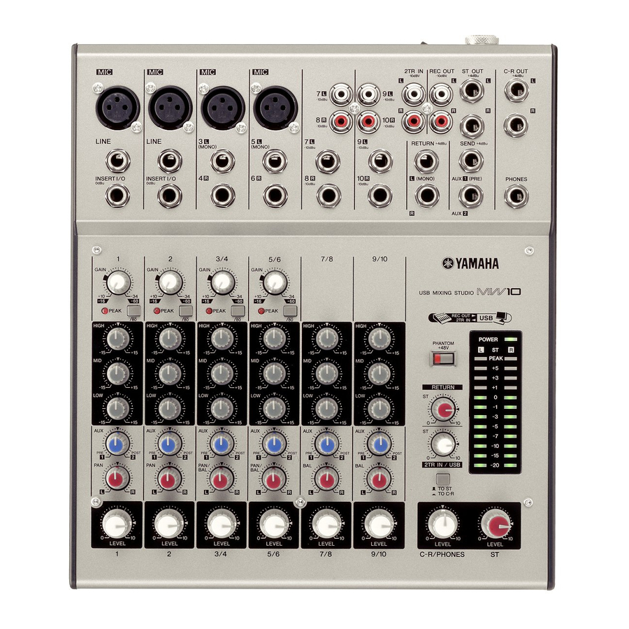
Page 9: Panel Layout(パネルレイアウト
All manuals and user guides at all-guides.com MW10 ■ PANEL LAYOUT(パネルレイアウト) ■ Channel Control Section(チャンネルコントロール部) Channels Channels Channels 1 and 2 3/4 and 5/6 (Monaural) (Stereo) (Stereo) [GAIN] Control [PEAK] Indicator ] Switch (High Pass Filter) Equalizer ([HIGH], [MID], and [LOW]) - Page 10 All manuals and user guides at all-guides.com MW10 ■ Input/Output Section(入出力部) !0 !0 Channel Input Jacks (CHs 1, 2, 3/4, 5/6) チャンネル INPUT 端子(CH 1、2、3/4、5/6) [MIC] jacks [MIC]端子 [LINE] jacks [LINE]端子 w [INSERT I/O]端子(CH 1、2) [INSERT I/O] Jacks (CHs 1 and 2) Channel Input Jacks (CHs 7/8, 9/10) チャンネル...
- Page 11 All manuals and user guides at all-guides.com MW10 Connector Polarities INPUT OUTPUT Pin 1: Ground MIC INPUT Pin 2: Hot (+) Pin 3: Cold (-) LINE INPUT (monaural channels), Tip: Hot (+) ST OUT, C-R OUT Ring: Cold (-) AUX1, AUX2 *...
-
Page 12: Disassembly Procedure(分解手順
All manuals and user guides at all-guides.com MW10 ■ DISASSEMBLY PROCEDURE(分解手順) Bottom Case ボトムケース (Time required: About 1 minute) (所要時間:約1分) Remove the two (2) screws marked [260]. (Fig.1) [260] のネジ2本を外します。 (Fig.1) Remove the five (5) screws marked [265] using a [265]... - Page 13 All manuals and user guides at all-guides.com MW10 MAIN Circuit Board MAINシート (Time required: About 14 minutes) (所要時間:約14分) Remove the bottom case. (See procedure 1.) ボ ト ムケース を外します。 ( 1項参照) Remove USB circuit board. (See procedure 2.) USBシー ト を外します。 ( 2項参照)...
- Page 14 All manuals and user guides at all-guides.com MW10 ト ッ プカバーを上に持ち上げ、 MAINシー ト (ノ ブ、 ボ タ ン、 ウ イ Lift up the top cover to remove the MAIN circuit board ン ド ウ METER付) を外 し ます。 ( Fig.2) (with knobs, button and Meter cover). (Fig.2) [265]...
- Page 15 All manuals and user guides at all-guides.com MW10 Power Switch and AC Connector 電源スイッチとACコネクター (Time required: About 4 minutes) (所要時間:約4分) Remove the bottom case. (See procedure 1.) ボ ト ムケース を外します。 ( 1項参照) Remove the one (1) screw marked [263], and pull out the [263]...
-
Page 16: Lsi Pin Description(Lsi 端子機能表
All manuals and user guides at all-guides.com MW10 ■ LSI PIN DESCRIPTION(LSI 端子機能表) PCM2900E/2K (X7143A00) USB PROTOCOL CONROLLER USB: IC101 NAME FUNCTION NAME FUNCTION USB differential input/output plus DAC analog output for R-channel USB differential input/output minus DAC analog output for L-channel... -
Page 17: Circuit Boards(シート基板図
All manuals and user guides at all-guides.com MW10 ■ CIRCUIT BOARDS(シート基板図) CONTENTS USB Circuit Board (X7196C0) ..................17 MAIN Circuit Board (X6347D0) .................. 18-21 MAIN Circuit Board (X6347E0) .................. 22-25 USB Circuit Board ● to MAIN-CN801 Component Side(部品側) Pattern Side(パターン側)... - Page 18 All manuals and user guides at all-guides.com MW10 MAIN Circuit Board (X6347D0) ● Apply sillicon grease to the shaded area. PHONES PHONES PHONES PHONES PHONES 斜線部にシリコングリスを塗る事。 C-R OUT C-R OUT C-R OUT C-R OUT C-R OUT C-R OUT C-R OUT...
- Page 19 All manuals and user guides at all-guides.com MW10 PEAK SCALE : 90/100 to USB-CN101 ONES ONES ONES ONES ONES PHANTOM PHANTOM RETURN RETURN 2TR IN/USB 2TR IN/USB +48V +48V C-R / PHONES TO ST TO ST TO C-R TO C-R...
- Page 20 All manuals and user guides at all-guides.com MW10 MAIN Circuit Board (X6347D0) ● Note: See parts list for details of circuit board component parts. 注:シートの部品詳細はパーツリストをご参照ください。...
- Page 21 All manuals and user guides at all-guides.com MW10 BROWN to AC ADAPTOR IN WD35000 Wiring Ass'y AC8 ON/STANDBY BLACK SCALE : 90/100 Pattern Side(パターン側) Note: See parts list for details of circuit board component parts. 2NA-WG23970 1 注:シートの部品詳細はパーツリストをご参照ください。...
- Page 22 All manuals and user guides at all-guides.com MW10 MAIN Circuit Board (X6347E0) ● Apply sillicon grease to the shaded area. PHONES 斜線部にシリコングリスを塗る事。 C-R OUT C-R OUT SEND ST OUT ST OUT RETURN RETURN L(MONO) The Electritic in he PWB silk shaded area is a thing fixed to he PWB with adhesives.
- Page 23 All manuals and user guides at all-guides.com MW10 PEAK SCALE : 90/100 to USB-CN101 ONES PHANTOM RETURN 2TR IN/USB +48V C-R / PHONES TO ST TO C-R 9/10 PAN/BAL PEAK PAN/BAL PEAK PEAK PEAK GAIN HIGH LEVEL Pattern Side(パターン側) Note: See parts list for details of circuit board component parts.
- Page 24 All manuals and user guides at all-guides.com MW10 MAIN Circuit Board (X6347E0) ● Note: See parts list for details of circuit board component parts. 注:シートの部品詳細はパーツリストをご参照ください。...
- Page 25 All manuals and user guides at all-guides.com MW10 BROWN to AC ADAPTOR IN WD35000 Wiring Ass'y AC8 ON/STANDBY BLACK SCALE : 90/100 Pattern Side(パターン側) Note: See parts list for details of circuit board component parts. 2NA-WG23970 1 注:シートの部品詳細はパーツリストをご参照ください。...
-
Page 26: Inspections(検査
All manuals and user guides at all-guides.com MW10 ■ INSPECTIONS Scope This inspection specification is applied to the mixer MW10. Power Supply The voltage is within +/-10%. AC Adaptor shall be used. Destination Voltage AC Adaptor 100V WC703400 120V WC703500... - Page 27 All manuals and user guides at all-guides.com MW10 MASTER control ● RETURN to ST level control : MAX 2TR IN/USB level control : MIN 2TR IN/USB switch : OFF (TO ST) C-R/PHONES level control : MAX ST Master VR : MAX Others ●...
- Page 28 All manuals and user guides at all-guides.com MW10 Table 3.3-5 Input Terminal RETURN L,R [dBu] INPUT INPUT Level ST L OUT ST R OUT L/MONO +4 +/-2 +4 +/-2 +4 +/-2 Table 3.3-6 Input Terminal 2TR IN L,R [dBu] INPUT...
- Page 29 All manuals and user guides at all-guides.com MW10 Channel Equalizer Characteristics In the state checked in 3.1 above, check the output level obtained at ST L OUT in the case of CH INPUT and ST CH INPUT L and at ST R OUT in the case of ST CH INPUT R when LO, HI and MID of INPUT are moved respectively.
- Page 30 All manuals and user guides at all-guides.com MW10 3.12 Maximum Output In the state 3.1, the distortion factor shall be less than 1% when the output level is +20dBu at ST L OUT, ST R OUT, AUX1 OUT, AUX2 OUT and C-R OUT.
- Page 31 All manuals and user guides at all-guides.com MW10 Inspections for USB Assembly Scope This inspection specification is appled to the USB assembly (WG644500). Power Source Measure by using Regulated DC Power Supply with two outputs of “+15V 0.1A or more” and “-15V 0.1A or more”.
- Page 32 MW10 power on or off, or connecting or disconnecting the USB cable. • Wait at least 6 seconds between turning the MW10 on or off, and between connecting or disconnecting the USB cable. When connecting or disconnecting the USB cable be sure to turn the 2TR IN/USB control all the way down.
- Page 33 All manuals and user guides at all-guides.com MW10 Launch Cubase LE Click [Control Panel] in the Device Setup window. The ASIO Multimedia Setup Click [Start] → [All Programs] → [Steinberg Cubase LE] → [Cubase LE] to launch the program. If the dialog window will appear.
- Page 34 All manuals and user guides at all-guides.com MW10 Select [VST Inputs] in the [Devices] menu. An empty 24-audio-track project window will appear. The VST Inputs window will open. Engage the Port [USB Audio CODEC] Active button ), and close the VST Inputs window.
- Page 35 [Show Inspector] button [Stereo Switch] button [Note] • The MW10 ST master fader does not affect the output level sent to the computer. • The Cubase LE channel strip fader only affects the playback output level from Cubase LE.(Make it to default(0) at the inspection.)
- Page 36 All manuals and user guides at all-guides.com MW10 Recording and Playback [Note] When a pair of headphones are plugged into the MW10 Click the Transport panel [Record] button PHONES jack, you can adjust the headphone listening to begin recording. level via the MW10 C-R/PHONES control and the 2TR IN/ When recording is started the project cursor will USB control.
- Page 37 All manuals and user guides at all-guides.com MW10 ■ 検査 適用範囲 ミキサーMW10について規定します。 電源 仕向地電源電圧の+/-10%以内 ACアダプターを使用します。 仕向 電圧 AC Adaptor 100V WC703400 120V WC703500 220V WC711000 220V WC703800 230V WC703700 230V WC703600 240V WC703900 本体の検査 準備 *USB AUDIOのアプリケーションソフト 以下の設定が可能なソフトウェアを使用して下さい。 (Cubase LE、TWEなど。Cubase LE Windows版での例は43ページを参照して下さい。) Sampling rate----48KHz or 44.1KHz Resolution--------16 bits...
- Page 38 All manuals and user guides at all-guides.com MW10 MASTER control ● RETURN to ST level control : MAX 2TR IN/USB level control : MIN 2TR IN/USB switch : OFF (TO ST) C-R/PHONES level control : MAX ST Master VR : MAX Others ●...
- Page 39 All manuals and user guides at all-guides.com MW10 Table 3.3-5 Input Terminal RETURN L,R [dBu] INPUT INPUT Level ST L OUT ST R OUT L/MONO +4 +/-2 +4 +/-2 +4 +/-2 Table 3.3-6 Input Terminal 2TR IN L,R [dBu] INPUT...
- Page 40 All manuals and user guides at all-guides.com MW10 チャンネルEQ変化特性 3.1の状態で、INPUT のLO、MID、HIをそれぞれ動かした時、CH INPUT及びST CH INPUT LはST L OUTに、ST CH INPUT RはST R OUTに得られる各周波数における出力レベルはEQ gain controlセンタークリック位置の出力レベルを 基準として[Table 3.7-1]の範囲内であることを確認します。 指定周波数において範囲内の出力レベルが得られない場合は、印加周波数を指定周波数の±20%の範囲で変化させ、 [Table 3.7-1]の変化幅が得られることを確認します。 Table 3.7-1 [dB] EQ control EQ GAIN Applied frequency Variation width 10kHz +12 +/-2 -12 +/-2 2.5kHz +15 +/-2 -15 +/-2 100Hz +12 +/-2 -12 +/-2 チャンネルセパレーション...
- Page 41 All manuals and user guides at all-guides.com MW10 3.12 最大出力 3.1の状態でST L OUT、ST R OUT、AUX1 OUT、AUX2 OUT、C-R OUTに+20dBu歪率1%以下の出力が得られること を確認します。 PHONES(L、R)に+7.5dBu歪1%以下の出力が得られることを確認します。 ST L OUT、ST R OUT測定時はPAN またはPAN/BAL、BAL controlをそれぞれL、Rに回しきって下さい。 C-R OUT、PHONE測定時はC-R/PHONE controlをMAXにして下さい。 3.13 入力換算雑音 3.1の状態で、CH INPUT MIC入力端子(2pin-Hotと3pin-Cold間)を150Ωで接続した時、ST L OUTで得られるノイズ レベルは-51.5dBu以下であることを確認します。 ノイズレベルが-51.5dBu以上の場合は、入力換算でのノイズレベルを求めそれが-127.5dBu以下であれば問題ありませ ん。 ST INPUT MIC入力端子(2pin-Hotと3pin-Cold間)を150Ωで接続した時、ST L OUT 得られるノイズレベルは-47.5dBu 以下であることを確認します。 ノイズレベルが-47.5dBu以上の場合は、入力換算でのノイズレベルを求めそれが-123.5dBu以下であれば問題ありませ ん。 (測定CH以外のLEVEL VRはMINにして下さい。また、ノイズ測定時は、12.7kHz・-6dB/octaveローパスフィルター を使用して下さい。) 3.14 残留雑音 3.1の状態で全てのINPUT部のCH VRをMINにします。 この時、MASTER部のVRを最大・最小にした時のノイズレベルは[Table 3.14-1]のレベル以下であることを確認しま す。 * AUXを測定する時は、全てのCH AUX Level controlはCENTERにして下さい。 * C-R OUT及びPHONESを測定する時は、ST VRはMINにして下さい。 (ノイズ測定時は、12.7kHz・-6dB/octaveローパスフィルターを使用して下さい。) Table 3.14-1 [dBu] STEREO OUT...
- Page 42 All manuals and user guides at all-guides.com MW10 USB Ass yの検査 適用範囲 USB Ass yについて規定します。USB Ass y(WG644500) 電源 +15V 0.1A以上、-15V 0.1A以上の2出力を持ったDC安定化電源を使用して測定して下さい。 準備 *USB AUDIOのアプリケーションソフト 以下の設定が可能なソフトウェアを使用します。 (Cubase LE、TWEなど。Cubase LE Windows版での例は43ページを参照して下さい。) サンプリングレート----48kHz or 44.1kHz レゾリューション-------16 bits *測定器の入力インピーダンスは100kΩ以上のこと。 *入力信号 特に指定の無い場合、入力信号は高品位サイン波とします。 *入出力 L Input : CN101-5pin R Input : CN101-6pin L Output : CN101-2pin R Output : CN101-3pin +15V : CN101-7pin -15V : CN101-9pin GND : CN101-8pin...
- Page 43 を確認します。 印加信号周波数を20kHzとした時の出力レベルは、1kHzを基準として-3 〜 -10dBの範囲内にあることを確認します。 4.5-3 ノイズレベル 4.5-1において、入力端子をGNDにショートしてUSB経由で録音、再生した時、出力端子のノイズレベルは-60dBu以 下であることを確認します。 *ノイズ測定時は、12.7kHz -6dB/octaveローパスフィルターを使用して下さい。 USB Audioアプリケーションソフト(Cubase LE Windows版)の設定例 Cubase LEのセットアップ USB端子ご使用時の注意 USB 端子とコンピューターを接続するときは、以下のことを行なってく ださい。 Cubase LEの再生音がそのまま録音されないよ 以下のことを行なわないと、コンピューターや本体が停止(ハングアップ) して、データが壊れたり、失われたりするおそれがあります。 うに、MW10の2TR IN/USB (TO ST/TO C-R) コンピューターやMW10本体が停止したときは、電源を入れ直し、コン スイッチを押してオン ( TO C-R) にしておき ピューターを再起動してください。 ます。 • USB端子とコンピューターを接続する前に、コンピューター C-R OUT端子とPHONE端子からは、再生音を の省電力(サスペンド/スリープ/スタンバイ/休止)モードを解除 してください。 モニターできます。 • MW10本体の電源を入れる前に、USB端子とコンピューター を接続してください。 • MW10本体の電源オン/オフやUSBケーブルの抜き差しをする 前に、コンピューターのすべてのアプリケーションを終了さ せてください。...
- Page 44 All manuals and user guides at all-guides.com MW10 デバイス設定ウィンドウの [コントロールパネ Cubase LEを起動します。 ル] をクリックします。ASIOマルチメディア基 [スタート] → [プログラム] → [Steinberg Cubase LE] 本設定ダイアログが表示されたら、 [詳細設定] → [Cubase LE] をクリックします。ASIOマルチメ ディアダイアログが表示される場合は、[はい]をク をクリックします。 リックします。 [デバイス] メニュー→ [デバイスの設定] を選択 して、デバイス設定ウィンドウを開きます。 左側の [デバイス] 欄で [VST Multitrack] を選択しま す。右側の [ASIOドライバ] で [ASIO Multimedia Driver]...
- Page 45 All manuals and user guides at all-guides.com MW10 [デバイス] メニューから [VST入力] を選択して ディレクトリの選択ダイアログが表示された VST入力ウィンドウを表示します。Port [USB ら、作成したプロジェクトファイルやオーディ オーディオデバイス]のActiveボタン をオン オファイルが保存されるフォルダーを指定し (このときブルーになります) にして、VST入力 て、 [OK] をクリックします。 ウィンドウを閉じます。 新規プロジェクトファイルを作成するには、 [ファイル] メニュー→ [新規プロジェクト] を選 択します。 新規プロジェクトダイアログが表示されます。 ここでは、テンプレートとして [24 Track Audio Recorder] を選択して、 [OK] をクリッ クします。...
- Page 46 All manuals and user guides at all-guides.com MW10 10. [プロジェクト] メニュー → [プロジェクトの設 インスペクターにある [ステレオ/モノラル] ボタ ンで、ステレオまたはモノラルを設定します。 定] をクリックします。 オンにするとステレオ 、オフにするとモノ ラル になります。ここでは、ステレオに設 定します。 [デバイス] メニュー→ [ミキサー] を選択してミ キサーウィンドウを表示します。 ミキサーウィンドウの左上にある矢印をクリックし て [広く] を選択して、各チャンネルストリップの表 示を広げます。ミキサーウィンドウは、録音が終わ るまで表示したままにしておくと便利です。 録音オン ボタン...
- Page 47 All manuals and user guides at all-guides.com MW10 通常は、ミキサーウィンドウのレベルメーター 録音/再生 が振り切れないように (0.0 dBにならないよう に) 、MW10本体のGAINコントロールとチャン トランスポートパネルの録音ボタンをクリック ネルフェーダーを調整します。 して、録音を開始します。 * 検査の場合はMAXに設定します。 録音が開始されると、プロジェクトカーソルが右に 動き始め、録音結果を示すボックスが作られます。 [Note] ・ MW10本体からコンピューターへの出力レベルは、 トランスポートパネル MW10のST マスターフェーダーでは調整できません。 ・ Cubase LE のチャンネルストリップ上のフェーダー は、Cubase LE からの出力レベルを調整するときに使 用します。 (検査の場合はデフォルト値 (0) を仕様しま 巻き戻し 録音 す。) 開始 早送り 停止 チャンネルストリップ上のピークレベル表示 (数値表示) で...
- Page 48 All manuals and user guides at all-guides.com <Page 1> IBLOCK DIAGRAM & LEVEL DIAGRAM MW10 PHANTOM +12V MAIN +48V SW102 Changeable width : ±15dB Lo : 100Hz (Shelving) PEAK(RED) Mid : 2.5KHz (peaking) Q101-104 LD102 LD101,201 Hi : 10KHz (shelving)
- Page 49 All manuals and user guides at all-guides.com <Page 2> IOVERALL CIRCUIT DIAGRAM 1/4 (MAIN 1/4) MW10 <Page 3 G2, Page 4 B5> OP AMP OP AMP <Page 3 G2, Page 4 C5> JK101 OP AMP JK102 JK103 OP AMP OP AMP...
- Page 50 All manuals and user guides at all-guides.com <Page 3> IOVERALL CIRCUIT DIAGRAM 2/4 (MAIN 2/4) MW10 JK501 <Page 2 H1, Page 4 B5> OP AMP OP AMP <Page 2 H1, Page 4 C5> OP AMP <Page 2 H1, Page 4 C5>...
- Page 51 All manuals and user guides at all-guides.com <Page 4> IOVERALL CIRCUIT DIAGRAM 3/4 (MAIN 3/4) MW10 to USB-CN101 <Page 5 F4> 28CC1-2000010510-3 1 (フ): Flame Proof Carbon Resistor(不燃化カーボン抵抗) Note : See parts list for details of circuit board component parts.
- Page 52 All manuals and user guides at all-guides.com <Page 5> IOVERALL CIRCUIT DIAGRAM 4/4 (MAIN 4/4, USB) MW10 MAIN USB CONTROLLER REGULATOR +15V REGULATOR REGULATOR -15V REGULATOR +12V REGULATOR +48V OP AMP OP AMP 28CC1-2000010510-4 28CC1-2001000913 to MAIN 3/4-CN801 <Page 4 D2>...
- Page 53 All manuals and user guides at all-guides.com PARTS LIST CONTENTS(目次) (目次) (目次) (目次) (目次) OVERALL ASSEMBLY (総組立) ..........2 ELECTRICAL PARTS(電気部品) ..........4 Note) DESTINATION ABBREVIATIONS Australian model Chinese model British model South-east Asia model Canadian model Taiwan model German model U.S.A.
- Page 54 All manuals and user guides at all-guides.com MW10 ■ OVERALL ASSEMBLY (総組立) Hexagon nut & Washer (六角ナット、ワッシャー) 400b 400a (x 4)
- Page 55 All manuals and user guides at all-guides.com MW10 PART NO. DESCRIPTION 部 品 名 REMARKS REF NO. QTY RANK OVWEALL ASSEMBLY 総 組 立 MW10 Overall Assembly 総 組 立 (WG20220) WG239700 Circuit Board MAIN (X6347D0) M A I N シ ー ト...
- Page 56 All manuals and user guides at all-guides.com MW10 ■ ELECTRICAL PARTS(電気部品) PART NO. DESCRIPTION 部 品 名 REMARKS REF NO. QTY RANK ELECTRICAL PARTS 電 気 部 品 MW10 WG239700 Circuit Board MAIN M A I N シ ー ト...
- Page 57 All manuals and user guides at all-guides.com MW10 PART NO. DESCRIPTION 部 品 名 REMARKS REF NO. QTY RANK V9726200 Electrolytic Cap. C208 470.00 6.3V ケ ミ コ ン US062470 Ceramic Capacitor-SL(chip) C209 470P 50V J RECT. チ ッ プ セ ラ ( S L )...
- Page 58 All manuals and user guides at all-guides.com MW10 PART NO. DESCRIPTION 部 品 名 REMARKS REF NO. QTY RANK V9726600 Electrolytic Cap. C343 47.00 25.0V ケ ミ コ ン V9726500 Electrolytic Cap. C345 10.00 25.0V ケ ミ コ ン V9726500 C346 Electrolytic Cap.
- Page 59 All manuals and user guides at all-guides.com MW10 PART NO. DESCRIPTION 部 品 名 REMARKS REF NO. QTY RANK V9726400 Electrolytic Cap. C463 100.00 16.0V ケ ミ コ ン US062100 Ceramic Capacitor-SL(chip) C464 100P 50V J RECT. チ ッ プ セ ラ ( S L )...
- Page 60 All manuals and user guides at all-guides.com MW10 PART NO. DESCRIPTION 部 品 名 REMARKS REF NO. QTY RANK V9726600 Electrolytic Cap. C633 47.00 25.0V ケ ミ コ ン US064100 Ceramic Capacitor-B (chip) C634 0.0100 50V K RECT. チ ッ プ セ ラ ( B )...
- Page 61 All manuals and user guides at all-guides.com MW10 PART NO. DESCRIPTION 部 品 名 REMARKS REF NO. QTY RANK V9726400 Electrolytic Cap. C855 100.00 16.0V ケ ミ コ ン US064100 Ceramic Capacitor-B (chip) C856 0.0100 50V K RECT. チ ッ プ セ ラ ( B )...
- Page 62 All manuals and user guides at all-guides.com MW10 PART NO. DESCRIPTION 部 品 名 REMARKS REF NO. QTY RANK V9812900 XLM Connector JK301 JACK XLR-301J-A キ ャ ノ ン コ ネ ク タ MIC(CH3) V9812600 Phone Jack JK302 ST MSJ-064-20B B ホ...
- Page 63 All manuals and user guides at all-guides.com MW10 PART NO. DESCRIPTION 部 品 名 REMARKS REF NO. QTY RANK WC529400 Transistor Q205 2SCKTC3875S-Y,GR-R ト ラ ン ジ ス タ VV556500 Transistor Q206 2SA1037AK Q,R,S TP ト ラ ン ジ ス...
- Page 64 All manuals and user guides at all-guides.com MW10 PART NO. DESCRIPTION 部 品 名 REMARKS REF NO. QTY RANK RD355680 Carbon Resistor (chip) R135 680.0 63M J RECT. チ ッ プ 抵 抗 RD356270 Carbon Resistor (chip) R136 2.7K 63M J RECT.
- Page 65 All manuals and user guides at all-guides.com MW10 PART NO. DESCRIPTION 部 品 名 REMARKS REF NO. QTY RANK RD358100 Carbon Resistor (chip) R247 100.0K 63M J RECT. チ ッ プ 抵 抗 RD357180 Carbon Resistor (chip) R248 18.0K 63M J RECT.
- Page 66 All manuals and user guides at all-guides.com MW10 PART NO. DESCRIPTION 部 品 名 REMARKS REF NO. QTY RANK RD358100 Carbon Resistor (chip) R359 100.0K 63M J RECT. チ ッ プ 抵 抗 RD356470 Carbon Resistor (chip) R360 4.7K 63M J RECT.
- Page 67 All manuals and user guides at all-guides.com MW10 PART NO. DESCRIPTION 部 品 名 REMARKS REF NO. QTY RANK RD355220 Carbon Resistor (chip) R457 220.0 63M J RECT. チ ッ プ 抵 抗 RD355220 Carbon Resistor (chip) R458 220.0 63M J RECT.
- Page 68 All manuals and user guides at all-guides.com MW10 PART NO. DESCRIPTION 部 品 名 REMARKS REF NO. QTY RANK RD356820 Carbon Resistor (chip) R610 8.2K 63M J RECT. チ ッ プ 抵 抗 RD357180 Carbon Resistor (chip) R611 18.0K 63M J RECT.
- Page 69 All manuals and user guides at all-guides.com MW10 PART NO. DESCRIPTION 部 品 名 REMARKS REF NO. QTY RANK RD357180 Carbon Resistor (chip) R820 18.0K 63M J RECT. チ ッ プ 抵 抗 RD354750 Carbon Resistor (chip) R821 75.0 63M J RECT.
- Page 70 All manuals and user guides at all-guides.com MW10 PART NO. DESCRIPTION 部 品 名 REMARKS REF NO. QTY RANK V8264700 Rotary Variable Resistor VR104 B 50.0K XV09213YNP ロ ー タ リ ー V R HIGH(CH1) V8264600 Rotary Variable Resistor VR105 A 20.0K XV09213YNP...
- Page 71 All manuals and user guides at all-guides.com MW10 PART NO. DESCRIPTION 部 品 名 REMARKS REF NO. QTY RANK UF037100 Electrolytic Cap. (chip) C125 10 16V チ ッ プ ケ ミ コ ン US126100 Ceramic Capacitor-F (chip) C126 1.0000 10V Z RECT.