Table of Contents
Advertisement
Quick Links
Contents .............................................................................................................................................1
Safety Information.............................................................................................................................2
Electrostatic Discharge Sensitive (ESDS) Device Handling .........................................................2
Theory of Operation ..........................................................................................................................3
Figure 1: PS1 signal flow Diagram ....................................................................................................3
Theory of Operation .................................................................................................................... 4-26
Figure 2. Personalized Amplification System
Figure 3. Powerstand Input and Output Connections .......................................................................5
Figure 4. R1 Remote Control ............................................................................................................5
Figure 5. DSP Functional Block Diagram .........................................................................................7
Figure 6. DC Power Supply Block Diagram ......................................................................................7
Table 1. Adjustable Controls: Gain range and nominal settings ......................................................12
Table 2. Nominal and Peak Signal Levels .......................................................................................13
Table 3. LED Trigger Levels ............................................................................................................14
Figure 7. Nominal Bass Configuration, 2 Bass Modules ................................................................14
Figure 8. Light Bass configuration ..................................................................................................15
Figure 9. External power stand, total of 4 bass modules ................................................................15
Figure 10. "Heavy" Bass, total of 8 bass modules ..........................................................................16
Table 4. Ideal and actual bass EQ gains .........................................................................................16
Table 5. EQ lookup table for all operational modes.........................................................................17
Table 6. Peripheral pins on the microcontroller ...............................................................................22
Figure 11. PS1 Tone Control Range ...............................................................................................24
Test Procedures ........................................................................................................................ 27-31
PS1 Power Stand Tests ...................................................................................................................27
Line Array Tests ...............................................................................................................................30
Bass Module Tests ..........................................................................................................................31
Appendix .................................................................................................................................... 32-48
PS1 Power Stand Software Update Procedure ............................................................................32
PS1 Power Stand Test Cables .................................................................................................. 33-34
1. Amplifier Output Test Cable .......................................................................................................33
2. XLR Microphone Input Test Cable .............................................................................................34
3. Line Input 1/4" Phono Jack Test Cable ......................................................................................34
4. Insert Jack Test Cable .................................................................................................................34
5. L1 Line Array Test Cables ...........................................................................................................35
6. Bass Module Test Cable .............................................................................................................35
IC Diagrams ............................................................................................................................... 36-48
CAUTION: The Bose
no user-serviceable parts. To prevent warranty infractions,
refer servicing to warranty service stations or factory service.
THIS DOCUMENT CONTAINS PROPRIETARY INFORMATION OF
BOSE CORPORATION WHICH IS BEING FURNISHED ONLY FOR
THE PURPOSE OF SERVICING THE IDENTIFIED BOSE PRODUCT
BY AN AUTHORIZED BOSE SERVICE CENTER OR OWNER OF
THE BOSE PRODUCT, AND SHALL NOT BE REPRODUCED OR
USED FOR ANY OTHER PURPOSE.
CONTENTS
Components ...........................................................4
®
PROPRIETARY INFORMATION
1
TM
contains
Advertisement
Table of Contents

Related Manuals for Bose Personalized Amplification System


Summary of Contents for Bose Personalized Amplification System
-
Page 1: Table Of Contents
THIS DOCUMENT CONTAINS PROPRIETARY INFORMATION OF BOSE CORPORATION WHICH IS BEING FURNISHED ONLY FOR THE PURPOSE OF SERVICING THE IDENTIFIED BOSE PRODUCT BY AN AUTHORIZED BOSE SERVICE CENTER OR OWNER OF THE BOSE PRODUCT, AND SHALL NOT BE REPRODUCED OR USED FOR ANY OTHER PURPOSE. -
Page 2: Safety Information
SAFETY INFORMATION 1. Parts that have special safety characteristics are identified by the symbol on schematics or by special notes on the parts list. Use only replacement parts that have critical characteristics recommended by the manufacturer. 2. Make leakage current or resistance measurements to determine that exposed parts are acceptably insulated from the supply circuit before returning the unit to the customer. -
Page 3: Theory Of Operation
THEORY OF OPERATION Figure 1: PS1 signal flow Diagram... -
Page 4: Theory Of Operation
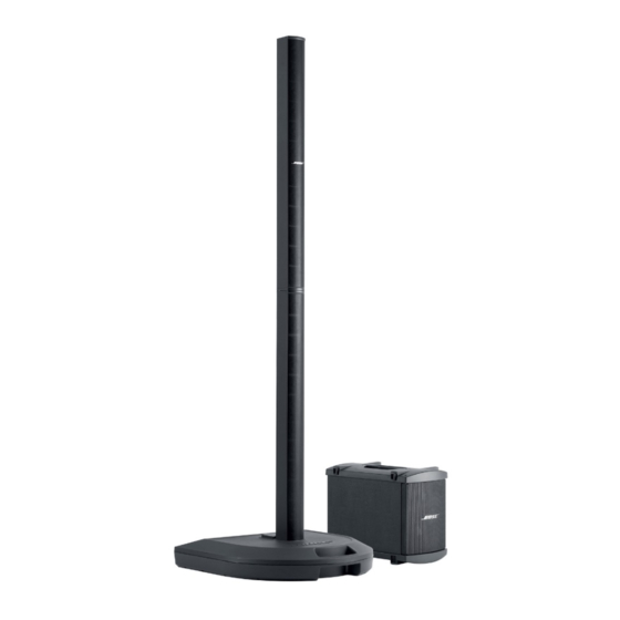
Radiator™ loudspeaker Remote control cable AC power cord B1 bass module 4-wire cable (blue) B1 bass module Figure 2. Personalized Amplification System Components The system has the following features: • All signal processing performed with DSP • Remote control •... - Page 5 THEORY OF OPERATION The system delivers 250W of output power for each of the three amplifiers housed in the power stand. The system uses a 110V / 230V AC power supply, and has a 1M ohm input impedance at the audio Ch1/Ch2 line input connector and 1.25k ohm input impedance at the audio Ch1/Ch2 MIC connector.
- Page 6 THEORY OF OPERATION Note: Refer to PS1 Power Stand schematic sheets in the service manual, reference number 264018-SM, for the following information. The information inside the brackets [ ] is the component’s grid location on the schematic sheet. The PS1 Power Stand combines the traditional functions of a mixer, digital controller (system EQ and limiter), power amplifier and mechanical speaker stand.
- Page 7 THEORY OF OPERATION DSP Processing Block Diag NoiseGate User EQ Preset EQ Ch1 In NoiseGate User EQ Preset EQ Ch2 In S-DATA Out (to SPDIF) Sys. EQ+X-Over, Hi Limiter Hi Out Ch 3 In Knee=+1.5dBV Ch 4 In Sys. EQ+X-Over, Lo Limiter Bass Out Master Vol.
- Page 8 THEORY OF OPERATION 110V AC is changed to about 300V DC, after passing through the EMI filter and the Diode Bridge. Then, the voltage signal is divided two ways: one DC voltage goes through the switch control & auxiliary circuit1 again, enters into the transformer primary1. The transformer1 has five secondary windings, the first outputs +24V DC (for the input panel), the second outputs +15V DC (for A/D, D/A buffer circuit), the third outputs –15V DC (for A/D, D/A buffer circuit), the fourth outputs +5V DC (for MCU and other ICs), the fifth outputs +3.3V DC (for DSP, A/D &...
- Page 9 THEORY OF OPERATION Relay DSP information to Remote The DSP needs to transfer the clip state, channel volume data (cause the table for channel volume in the DSP), and the system working status to the MCU. The communication adopts software simulation UART, with two I/O pins as RX and TX. The communication rate is 4800bps, add a start bit and stop, so every sending byte has 10 bits.
- Page 10 THEORY OF OPERATION Bass module sensing circuitry On the bass connector, there are four pins. 1+ and 1- outputs bass signal, 2+ and 2- is used to check the number of bass modules connected to the power stand. When there is no bass module connected, the resistance value between 2+ and 2- is greater than 10k ohms, when one bass module is connected to the power stand, the resistance between 2+ and 2- is equal to 10k ohms, when two bass modules are connected, the resistance value between 2+ and 2- is equal...
- Page 11 THEORY OF OPERATION The DSP, U461 [DSP PCB sheet 3, B4] is an Analog Devices 21065L general purpose floating point digital signal processor. There are two of these DSP ICs used in the system. Each is capable of about 40MIPs of performance. The DSPs are mainly used to process sound effects. They provide: •...
- Page 12 THEORY OF OPERATION 1.2 Gain Specifications 1.2.1 Purpose and Philosophy ® The purpose of this specification is to define all relevant gain levels in the Bose Personalized Amplification System™ Power Stand and to specify procedures, for how these gains can be measured.
- Page 13 THEORY OF OPERATION Point Nominal Peak Comment Line In, Trim -30dBV un- - 12 dBV Ch1 / Ch2 Vol. + Master @ 12:00. Maximum input @ Max limited by input INA163 output clipping. Line In, Trim -1dBV dBV +17 dBV Ch1 / Ch2 Vol.
- Page 14 THEORY OF OPERATION 1.2.3 LED Trigger Level The system has also two signal/clip LED indicators. The signal LED should turn on as soon as the level reaches -30 dB versus nominal level and the clip LED should light at +6 dB versus nominal level.
- Page 15 THEORY OF OPERATION Light Bass Figure 8. Light Bass configuration External Power Stand External Power Stand With 2 Bass Modules With 2 Bass Modules Bass Bass All Amps All Amps Send Send Figure 9. External power stand, total of 4 bass modules...
- Page 16 THEORY OF OPERATION External Power Stand With 6 Bass Modules Bass All Amps Send Figure 10. “Heavy” Bass, total of 8 bass modules Ideally, at low levels all bass configurations should produce the same spectral balance, and the main difference between the “light” system and the “heavy” system should be that the “heavy” system can produce 18dB more SPL before the limiter kicks in.
- Page 17 THEORY OF OPERATION 1.3.2 Implementation The power stands detects: a) The number of bass modules B1 connected to “Amp3 out”. This is done by measuring the impedance between pins 2+ and 2- of the “Amp 3 out” connector. The B1 bass module has a 10k ohm resistor between those to pins.
- Page 18 THEORY OF OPERATION 1.4 Power Supply Electronics The PS1 is powered by a total of four distinct switch-mode power supplies. All of these are fed approximately 340VDC from the single input filter PC Board which contains numerous EMI filtering components, in addition to a bridge rectifier and storage capacitors C607 and C608 [FCC Filter PCB sheet1, C4].
- Page 19 THEORY OF OPERATION Input “combo-jacks” J101 and J102 [C1, A1] are configured so that outputs from buffer amps U101A & U103A are shorted to ground when a ¼” plug is not inserted into J101 or J102 – this eliminates the OpAmps’s noise contribution when the Mic input is in use, or when the channel is not being used.
- Page 20 THEORY OF OPERATION 1.5.8 Digital to Analog Converter (Analog) The stereo D/A converter U387 [B5] is of type Crystal CS4392. It has two symmetrical outputs that get turned into an unbalanced signal through difference amplifier U388A [D7] /U388B [B7]. These OpAmp sections also form additional 2-pole low-pass filters that help remove out-of-band components from the audio output.
- Page 21 (= 256*48kHz) oscillator. XTAL431 [DSP PCB sheet 2, B3] and distributed through U434 [B5]. The PS1 can receive SPDIF through the DATA In connector, but this data is received asynchro- nously to the actual audio data. This is different from most other Bose ®...
- Page 22 THEORY OF OPERATION 1.7 Digital Signal Processor 1.7.1 Architecture The DSP is an Analog Devices ADSP21065L processor. It boots from an EEPROM SST20LE020, U462 [DSP PCB sheet 3, C7]. U462 accessed through boot memory space and through external memory space 3. Either BMS or MS3 on the DSP will chip enable U462 and then a standard write/read enable interface is used to address U462.
- Page 23 1.9 Software and User Interface The Bose ® Personalized Amplification System™ family of products has a simple user interface which is mostly implemented in software. In this chapter we describe how most of the functions are implemented. 1.9.1 Gain Staging Gain staging is the process of properly adjusting the gain of the system.
- Page 24 THEORY OF OPERATION P S1 tone controls P S1 tone controls P S1 tone controls Fre quenc y (hertz) Fre quenc y (hertz) Fre quenc y (hertz) Figure 11. PS1 Tone Control Range 1.9.4 Master Volume The microcontroller polls the remote in regular intervals. The microcontroller transfers the mas- ter volume setting to the DSP which implements them for each channel as shown in Figure 5.
- Page 25 THEORY OF OPERATION 1.10 Power Cycling 1.10.1 Power Up When power is first applied, 110V AC is applied to the primary side of the transformer1, and at the secondary side of the transformer1 will charge up +24V, +15V, -15V, +5V, +3.3V. And after 7 ms, they become stable almost at the same time.
- Page 26 2 bass modules connected, and again, adjusts the output level and EQ accordingly. If the PS1 sees an infinite resistance, it knows that there is no bass module connected and adjusts accordingly. The woofers in the bass module are replaceable. The input panel, grille and Bose logo are also replaceable.
-
Page 27: Test Procedures
TEST PROCEDURES PS1 Power Stand Tests 1.3 Using a balanced XLR male input cable, apply a 1 kHz, -30dBV signal to the channel 1 input. Equipment Required • dB Meter 1.4 Reference a dB meter to the input level. • Digital Multi-meter Measure the gain output at the Amp 1 OUT •... - Page 28 TEST PROCEDURES 3. Channel 1 and 2 Mic Input Signal to 4.4 Reference a dB meter to the input level. Noise Ratio (Dynamic Range) Tests Measure the gain output at the Amp 1 OUT jack. It should be +28.5 dB + 4dB. 3.1 Place a 1/4”...
- Page 29 TEST PROCEDURES 6. Channel 1 and 2 Line Input Signal to 8. Channel 3 and 4 Line Input Frequency Noise Ratio (Dynamic Range) Tests Reponse and Distortion Tests 6.1 Place a 1/4” mono shorting plug into the 8.1 Place a 1/4” mono shorting plug into the Amp 2 IN and Amp 3 IN jacks on the right Amp 1 IN and Amp 2 IN jacks on the right hand side of the input/output panel.
-
Page 30: Line Array Tests
TEST PROCEDURES 9.4 Reference a dB meter to the output level Note: To distinguish between normal sus- at the Bass/Amp 3 OUT jack. Remove the pension noise and rubs or ticks, displace the input signal and measure the A-Weighted cone slightly with your fingers. If the noise output level. -
Page 31: Bass Module Tests
TEST PROCEDURES Bass Module Tests 3. Transducer Phase Test 3.1 Momentarily apply a DC voltage of 10V, Connect the Bass Module under test to an positive applied to the positive terminal of amplifier using the test cables described in the test cable and GND connected to the the appendix of this troubleshooting guide. -
Page 32: Appendix
PS1 Power Stand Software Update Procedure Required Equipment: ® ® 1- CD player with a S/PDIF digital output (do not use a Bose Lifestyle media center) 1- PS1 Power Stand update CD (see the instructions for creating this disc below) -
Page 33: Ps1 Power Stand Test Cables
APPENDIX PS1 Power Stand Test Cables Note: In order to be able to properly test the PS1 Power Stand, you will need to make up a few test cables. 1. Amplifier Output Test Cable: Parts needed: ® ® 1- Neutrik NL4FX Speakon X-Line/4 Pole connector. -
Page 34: Xlr Microphone Input Test Cable
APPENDIX PS1 Power Stand Test Cables (continued) 2. XLR Microphone Input Test Cable Parts needed: 1 - XLR male connector 1 - Dual banana jack 18 AWG shielded twisted pair wire, 6 feet This cable is used to test the channel 1 and 2 microphone inputs on the PS1 Power Stand. These input jacks are dual purpose jacks that will accept either XLR or 1/4”... -
Page 35: L1 Line Array Test Cables
APPENDIX 5. L1 Line Array Test Cables These two cables will allow you to test the upper and lower line array sections without a PS1 power stand. Use these cables for the line array test procedures in this service manual. Lower Line Array Section Test Cable Parts needed: 1 - 10 pin Molex male connector, Molex part... -
Page 36: Ic Diagrams
APPENDIX 32 31 30 1. Output1 2. Inverting input1 3. Non-inverting input 1 32-lead PLCC 4. -Vcc Top View 5. Non-inverting input 2 6. Inverting input 2 7. Output 2 8. +Vcc 14 15 16 17 18 19 20 29LE020 EEPROM Pinout Diagram TLO72, Dual Op-Amp ESCRIPTION Sym bol... - Page 37 APPENDIX PIN CONFIGURATION LOGIC SYMBOL 74LV08 Quad AND Gate 74HC00, Quad 2 Input Nand Gate Pin A ssign ment s for SOIC and DIP Top View 74LCX125 Quad Buffer CD4093BC Quad NAND Gate PIN DESCRIPTION PIN NUMBER SYMBOL NAME AND FUNCTION 1, 4, 9, 12 1A ±...
- Page 38 APPENDIX 208-LEAD MQFP PIN RSF0 PIN 1 IDENTIFIER RCLK0 DR0A BSEL DR0B TFS0 TCLK0 TRST DT0A DT0B RFS1 RCLK1 DR1A DR1B TFS1 TCLK1 FLAG4 FLAG5 FLAG6 DT1A DT1B FLAG7 PWM EVENT1 DATA31 DATA30 PWM EVENT0 ADSP-21065L TOP VIEW (Not to Scale) DATA29 CLKIN DATA28...
- Page 39 APPENDIX Dual-In-Line Package D R Q Connection Diagram and Truth Table (No change) Level change Don't care case CD4015BC Static Shift Register Pin A ssign ment s for SOIC and DIP Top View CD4093BC Quad Nand Gate CS4392-KZ Digital to Analog Converter (DAC) INA163 Ð...
- Page 40 APPENDIX AMP 2 Anode Cathode AMP 1 Emitter Collector NJM78L05 Op-Amp PC817A Photocoupler CHANNEL IN/OUT BINARY COMMON OUT/IN LOGIC 1 OF 8 LEVEL DECODER CONVERSION WITH ENABLE Functional Dia gram TRUTH TABLE INPUT STATES ÒONÓ ENABLE CHANNELS TOP VIEW CHANNEL IN/OUT COM OUT/IN CHANNEL...
- Page 41 APPENDIX P1.0-P1.5 T0, T1CK, T1, P0.0-P0.7 BUZ, RxD, TxD BLOCK DIAGRAM Basic Port 0 Port 1 Timer P1.4/RxD P0.1 P1.5/TxD P0.0 P3.7/ADC7 SDAT/P4.3 P2.0-P2.7 Port 2 S3P8475 Port I/O and Interrupt P3.6/ADC6 SCLK/P4.2 INT0-INT7 T0(CAP) Control P3.5/ADC5 Timer 0 (44-QFP) T0(PWM) P3.4/ADC4 P3.3/ADC3...
- Page 42 APPENDIX TC9459F L-OUT R-OUT L-IN R-IN L-ch R-ch L-LD1 R-LD1 L-LD2 R-LD2 L-A-GND R-A-GND DATA TC9459F Volume Control IC...
- Page 43 APPENDIX TO-92 (TO-226) Pin 1. Reference 2. Anode 3. Cathode UC2842 PWM Controller Pinout Diagram TL431CLP (TO-92) BLOCK DIAGRAM Note 1: Toggle flip flop used only in 1844 and 1845. UC2842 PWM Controller Block Diagram...
- Page 44 APPENDIX CS5361 AD Converter Pinout and Table...
- Page 45 APPENDIX CS8406 Digital Audio Interface Transmitter...
- Page 46 APPENDIX CS8416 Digital Audio Interface Receiver...
- Page 47 APPENDIX TDA8929T Digital Amplifier Controller...
- Page 48 APPENDIX TDA8927J Digital Power Amplifier...
-
Page 49: Personalized Amplification System
Personalized Amplification System Troubleshooting Guide ©2004 Bose Corporation Troubleshooting Guide Reference Number 264018-TG Rev. 00... - Page 50 SPECIFICATIONS AND FEATURES SUBJECT TO CHANGE WITHOUT NOTICE Bose Corporation The Mountain Framingham Massachusetts USA 01701 P/N: 264018-TG Rev. 00 10/2004 (P) http://serviceops.bose.com...