Advertisement
Quick Links
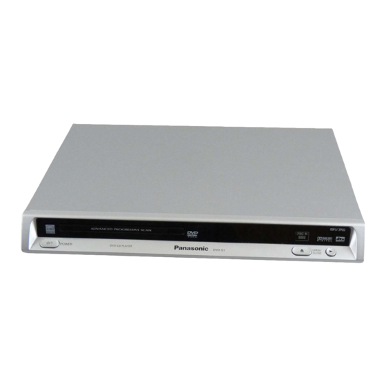
SPECIFICATIONS
PDF created with pdfFactory Pro trial version
DVD-S1E / DVD-S1EB / DVD-S1EG
Specifications
Power supply:
Power consumption:
Power consumption in standby mode:
Dimensions:
Mass:
Signal system:
Operating temperature range:
Operating humidity range:
Discs played [8 cm (3 " ) or 12 cm (5 " )]:
(1)
DVD (DVD-Video)
(2)
DVD-R (DVD-Video, MP3*2,4, JPEG*3,4)
(3)
DVD-RW (DVD-Video, MP3*2,4, JPEG*3,4)
(4)
+R/+RW (Video)
(5)
CD, CD-R / CD-RW (CD-DA, Video CD, SVCD*1, MP3*2,4,
JPEG*3,4)
(6)
DVD-R DL (DVD-Video)
(7)
+R DL (Video)
*1
Conforming to IEC62107
*2
MPEG-1 Layer 3, MPEG-2 Layer 3
*3
Exif Ver2.1 JPEG Baseline files
Picture resolution: between 320 × 240 and 6144 × 4096
pixels (Sub sampling is 4:2:2 or 4:2:0)
www.pdffactory.com
ORDER NO.CHM0604019CE
DL4.5 Mechanism Series
(S).......................Silver Type
AC230-240 V, 50 Hz
(DVD-S1EB)
AC230 V, 50 Hz
(DVD-S1E/EG)
10 W
approx. 1 W
360 (W) × 251 (D) × 43 (H) mm
1.8 kg (approx.)
PAL 625/50, PAL 525/60, NTSC
+ 5 to + 35 °C
5 to 90 % RH (no
condensation)
1
DVD Player
Color
Advertisement

Related Manuals for Panasonic DVD-S1E


Summary of Contents for Panasonic DVD-S1E
- Page 1 ORDER NO.CHM0604019CE DVD Player DVD-S1E / DVD-S1EB / DVD-S1EG DL4.5 Mechanism Series Color (S).......Silver Type SPECIFICATIONS Specifications Power supply: AC230-240 V, 50 Hz (DVD-S1EB) AC230 V, 50 Hz (DVD-S1E/EG) Power consumption: 10 W Power consumption in standby mode: approx. 1 W Dimensions: 360 (W) ×...
- Page 2 The total combined maximum number of recognizable audio and picture contents and groups: 1000 audio and picture contents and 256 groups. Video output: Output level: 1 Vp-p (75 Output terminal: Pin jack (1 system)/AV S video output: Y output level: 1 Vp-p (75 C output level: NTSC: 0.286 Vp-p (75...
- Page 3 Laser power: CLASS 1 / CLASS 3A Note: Specifications are subject to change without notice. Mass and dimensions are approximate. Solder: This model uses lead free solder (PbF). 2006 Matsushita Electric Industrial CO., Ltd. All rights reserved. Unauthorized copying and distribution is a violation of law. 1.
- Page 4 jumpered AC plug and each exposed metallic cabinet part on the equipment such as screwheads, connectors, control shafts, etc. When the exposed metallic part has a return path to the chassis, the reading should be between 1M and 5.2M . / When the exposed metal does not have a return path to the chassis, the reading must be .
- Page 5 Some semiconductor (solid state) devices can be damaged easily by static electricity. Such components commonly are called Electrostatically Sensitive (ES) Devices. Examples of typical ES devices are integrated circuits and some field-effect transistorsand semiconductor "chip" components. The following techniques should be used to help reduce the incidence of component damage caused by electro static discharge (ESD).
- Page 6 together of your clothes fabric or the lifting of your foot from a carpeted floor can generate static electricity (ESD) sufficient todamage an ES device). 3. PRECAUTION OF LASER DIODE 4. SERVICE CAUTION BASED ON LEGAL RESTRICTIONS 4.1. General description about Lead Free Solder (PbF) The lead free solder has been used in the mounting process of all electrical components on the printed circuit boards used for this equipment in considering the globally environmental conservation.
- Page 7 - The lead free solder has to be used when repairing the equipment for which the lead free solder is used. (Definition: The letter of “PbF” is printed on the PCB using the lead free solder.) - To put lead free solder, it should be well molten and mixed with the original lead free solder.
- Page 8 1. Use the anti-static wrist strap to discharge the static electricity form your body. 5.1.3. Handling of optical pickup 1. To keep the good quality of the optical pickup maintenance parts during transportation and before installation, the both ends of the laser diode are short-circuited.
- Page 9 6.2. Casing Parts and P.C.B. Positions 6.3. Top Panel 1. Unscrew the screws. PDF created with pdfFactory Pro trial version www.pdffactory.com...
- Page 10 6.4. Front Panel 1. Release the connector. 2. Release the tabs. 6.5. Front angle and Operation P.C.B. and Power SW P.C.B. 1. Unscrew the screws. PDF created with pdfFactory Pro trial version www.pdffactory.com...
- Page 11 6.6. Module P.C.B. 1. Remove the connectors. 2. Unscrew the screws. 3. Press each tab with the nipper to module P.C.B. vertically. 6.7. Mechanism Unit 1. Unscrew the screws. 2. Release the tabs. PDF created with pdfFactory Pro trial version www.pdffactory.com...
- Page 12 6.8. Rear panel 1. Unscrew the screws. 2. Release the tabs. 6.9. Mother P.C.B. 1. Unscrew the screws. PDF created with pdfFactory Pro trial version www.pdffactory.com...
- Page 13 6.10. Service Position 6.10.1. Servicing position of the Module P.C.B. 6.10.2. Servicing position of the Mother P.C.B. PDF created with pdfFactory Pro trial version www.pdffactory.com...
- Page 14 6.10.3. List of the Extension Cables 7. ASSEMBLING AND DISASSEMBLING THE MECHANISM UNIT 7.1. Disassembly Procedure PDF created with pdfFactory Pro trial version www.pdffactory.com...
- Page 15 7.2. Traverse Unit 1. Slide the lever (A) in the arrow direction (to the opposite side) till it stops. 2. Slide the lever (A) further by bending the tab at the right side of the lever A in the right direction. (The right groove opens and the boss becomes seen.) 3.
- Page 16 7.3. Tray 1. Slide the guide tray unit while pressing the stopper in the arrow direction, and remove the guide tray unit. 2. Raise the loading unit. 3. Slide the lever in the arrow direction till it stops and pull the tray out.
- Page 17 4. Spread the tabs at the both sides and pull the tray out. (The tray slides a little forward and stops.) 5. Remove the drive arm concave phase from the tray slider and tray. <Assembling the tray unit> 1. Insert a part of the tray into the unit sliding over the groove on the PDF created with pdfFactory Pro trial version www.pdffactory.com...
- Page 18 mechanical chassis unit. 2. Insert the tray to the point before the tab of the mechanical chassis unit. 3. Hook the drive arm concave phase over the tray and the tray slider. 4. Press in the tray. 5. Make sure that the tray and the drive arm move smoothly. 7.4.
- Page 19 2. Hook the lock lever spring on the lock lever projection part temporarily. 3. Unlock the tab and remove the lock lever. 4. Remove the belt. 5. Unlock the tab and remove the pulley. PDF created with pdfFactory Pro trial version www.pdffactory.com...
- Page 20 6. Remove the relay gear. 7. Turn the change lever in the arrow direction till it stops. 8. Hook the change lever spring on the change lever project part temporarily. 9. Pull the lever (B) in the bottom side to your side and remove the change lever.
- Page 21 10. Remove the drive rack, the sub rack and the drive gear. 7.5. Loading motor P.C.B. 1. Unscrew the screws. PDF created with pdfFactory Pro trial version www.pdffactory.com...
- Page 22 7.6. TRV Unit 7.6.1. Cautions to Be Taken in Handling the TRV Unit The laser diode in the TRV unit may be damaged due to electrostatic discharge generating from clothes or human body. Use due caution to electrostatic discharge damage when servicing the laser diode.
- Page 23 7.6.2. Procedure for Disassembling the TRV Unit Notice 1. This section aims to focus on the disassembling methods of some parts in the case that no damage is occurred to optical pickup units. 2. When the optical pickup unit is defective, the overall traverse unit needs replacement.
- Page 24 2. Remove the connecter, take out the 22P FFC. After changing the 22P FFC, please remove the solder. (refer to Fig. B) 3. Push the tabs on the back and remove the TRV Gear B and A. PDF created with pdfFactory Pro trial version www.pdffactory.com...
- Page 25 4. Unscrew the screws. 5. Remove the drive rack. Caution Do not dissemble drive rack fixing screws repeatly, otherwise the screws may hard to tighten and affect the accuracy of optical pickups consequently. 6. Remove the solders of the SP motor and the TRV motor. PDF created with pdfFactory Pro trial version www.pdffactory.com...
- Page 26 7. Unscrew the screws, then remove the TRV Motor and TRV SW P.C.B. Unit. <Assembling the TRV unit> 1. After replacing the TRV Unit and connecting the 22P FFC, remove the solder on the optical pickup unit. PDF created with pdfFactory Pro trial version www.pdffactory.com...
- Page 27 Caution 1. Do not give a considerable shock to the optical pickup unit as it has an extremely high-precise structure. 2. Do not touch the lens in the optical pickup unit. 2. The FFC is fixed as shown below. 8. SELF-DIAGNOSIS FUNCTION AND SERVICE MODES 8.1.
- Page 28 The service modes can be activated by pressing various button combination on the player and remote control unit. please carry out your operation based on the remote control supplied with Panasonic DVD player of previous models. PDF created with pdfFactory Pro trial version...
- Page 29 Player buttons Remote control unit Application Note buttons PLAY Displaying the UHF display F_ _ _ Refer to 8.3. Self- Diagnosis OPEN/CLOSE Function Display). Jitter check, tilt adjustment *Display shows J_xxx/yyy_zz "yyy" and "zz" shown to the right have nothing to do with the jitter value.
- Page 30 Error Error Content Additional error explanation Defect 1 Defect 2 Defect 3 Code Focus error Focus coil, FE singal error TRV Unit DV4.1 (IC8001) Tray loading error LD motor error, DV4.1 (IC8001) error LD IC8251 Motor Spindle servo (Spindle servo, DV4.1 (IC8001) SP DV4.1 error motor, CLV servo error)
- Page 31 Pressing various button combinations on the player and remote control unit can activate the service modes. Please carry out your operation based on the remote control supplied with Panasonic DVD player of previous models. PDF created with pdfFactory Pro trial version...
- Page 32 8.6. Sales demonstration lock function This function prevents discs from being lost when the unit is used for sales demonstrations by PDF created with pdfFactory Pro trial version www.pdffactory.com...
- Page 33 disabling the disc eject function. "LOC" is displayed on the unit, and ordinary operation is disabled. 8.6.1. Setting The sales demonstration lock is set by simultaneously pressing PLAY and OPEN/CLOSE buttons on the player and QUICK REPLAY button on the remote control unit for 1 second or longer.
- Page 34 Make sure to select normal format instead of image format. If you may not be able to complete a downloding from the TSN-WEB page, please obtain the file through your local Panasonic Service Organization. - Updating firmware 1. Load the version-up disc that is supplied to the player and run it.
- Page 35 Application Name Number Inspection Extension cable (module P.C.B. to mother VUC8026 P.C.B.) Extension cable (module P.C.B. to mother RFKZ0106 P.C.B.) Others Hanarl VFK1784 Grease RFKXPG641 Drysurf RFKXGUD24 Confirmation CD test disc PVCD-K06 or any other commercially available disc VCD test disc PVCD-K06 or any other commercially available disc DVD test disc...
- Page 36 INITIAL/LOGO ABBREVIATIONS A0~UP ADDRESS ACLK AUDIO CLOCK AD0~UP ADDRESS BUS ADATA AUDIO PES PACKET DATA ADDRESS LATCH ENABLE AMUTE AUDIO MUTE AREQ AUDIO PES PACKET REQUEST AUDIO RF SERVO AMP INVERTED INPUT SERVO AMPOUTPUT ASYNC AUDIO WORD DISTINCTION SYNC BIT CLOCK (PCM) BCKIN BIT CLOCK INPUT BLACK DROP OUT...
- Page 37 INITIAL/LOGO ABBREVIATIONS DACCK D/A CONVERTER CLOCK DEEMP DEEMPHASIS BIT ON/OFF DEMPH DEEMPHASIS SWITCHING DIG0~UP FL DIGIT OUTPUT DATA INPUT DMSRCK DM SERIAL DATA READ CLOCK DMUTE DIGITAL MUTE CONTROL DROP OUT DOUT0~UP DATAOUTPUT DATA SLICE RF (BIAS) DROP OUT SIGNAL DRPOUT DATA REQUEST DREQ...
- Page 38 INITIAL/LOGO ABBREVIATIONS IECOUT IEC958 FORMAT DATA OUTPUT IPFRAG INTERPOLATION FLAG IREF I (CURRENT) REFERENCE ISEL INTERFACE MODE SELECT LDON LASER DIODE CONTROL LASER POWER CONTROL LRCK L CH/R CH DISTINCTION CLOCK MA0~UP MEMORY ADDRESS MEMORY CLOCK MCKI MEMORY CLOCK INPUT MCLK MEMORY SERIAL COMMAND CLOCK...
- Page 39 INITIAL/LOGO ABBREVIATIONS READ ENABLE RFENV RF ENVELOPE RF PHASE DIFFERENCE OUTPUT (CD-ROM) REGISTER SELECT RSEL RF POLARITY SELECT RESET RESERVE SBI0, 1 SERIAL DATA INPUT SBO0 SERIAL DATA OUTPUT SBT0, 1 SERIAL CLOCK SERIAL DATA CLOCK SCKR AUDIO SERIAL CLOCK RECEIVER SERIAL CLOCK SCLK...
- Page 40 SUB CODE Q DATA SYSCLK SYSTEM CLOCK INITIAL/LOGO ABBREVIATIONS TRACKING ERROR TIBAL BALANCE CONTROL BALANCE OUTPUT 1 BALANCE INPUT BALANCE INPUT BALANCE OUTPUT 2 TPSN OP AMP INPUT TPSO OP AMP OUTPUT TPSP OP AMP INVERTED INPUT TRCRS TRACK CROSSSIGNAL TRON TRACKING ON TRSON...
- Page 41 INITIAL/LOGO ABBREVIATIONS X' TAL XALE X ADDRESS LATCH ENABLE XAREQ X AUDIO DATA REQUEST XCDROM X CD ROM CHIP SELECT X CHIP SELECT XCSYNC X COMPOSITE SYNC X DATA STROBE XHSYNCO X HORIZONTAL SYNC OUTPUT XHINT XH INTERRUPTREQUEST X' TAL OSCILLATOR INPUT XINT X INTERRUPT X MEMORY WRITE ENABLE...
- Page 42 13.1. OVERALL BLOCK DIAGRAM 13.2. POWER SUPPLY BLOCK DIAGRAM 13.3. SERVO BLOCK DIAGRAM 13.4. VIDEO BLOCK DIAGRAM 13.5. AUDIO BLOCK DIAGRAM 14. INTERCONNECTION SCHEMATIC DIAGRAM & SCHEMATIC DIAGRAM NOTES 14.1. INTERCONNECTION SCHEMATIC DIAGRAM 14.2. SCHEMATIC DIAGRAM NOTES This schematic diagram may be modified at any time with the development of new technology. Important safety notice: Components identified by mark have special characteristics important for safety.
- Page 43 15.2. FRONT & AV OUT SECTION (MOTHER P.C.B. (2 / 2)) SCHEMATIC DIAGRAM 15.3. MODULE SCHEMATIC DIAGRAM 16. PRINT CIRCUIT BOARD 16.1. MOTHER P.C.B. 16.2. MOTHER P.C.B. ADDRESS INFORMATION 16.3. MODULE P.C.B. (1/2) 16.4. MODULE P.C.B. (2/2) 16.5. MODULE P.C.B. ADDRESS INFORMATION 17.
- Page 44 17.2. MECHANISM SECTION EXPLODED VIEW PDF created with pdfFactory Pro trial version www.pdffactory.com...
- Page 45 17.3. PACKING & ACCESSORIES SECTION EXPLODED VIEW PDF created with pdfFactory Pro trial version www.pdffactory.com...
- Page 46 18. REPLACEMENT PARTS LIST Notes: *Important safety notice: Components identified by mark have special characteristics important for safety. Furthermore, special parts which have purposes of fire-retardant (resistors), high-quality sound (capacitors), low-noise (resistors), etc. are used. When replacing any of components, be sure to use only manufacture’s specified parts shown in the parts list.
- Page 47 *”(IA)-(ID)”, marks in Remarks indicate languages of instruction manuals. [(IA): English, (IB): Polish, (IC): German/ Italian/ French, (ID): Netherlands/ Swedish/ Danish] *All parts except parts mentioned [SPC] in the Remarks column are supplied by PAVCSG. *Parts mentioned [SPC] are supplied by PAVC-CSG. Ref.
- Page 48 Ref. No. Part No. Part Name & Description Remarks RHD30007-1SJ SCREW RXQC0006 TRV UNIT ASS'Y 101-1 RDGC0002 TRV GEAR A 101-2 RDGC0003 TRV GEAR B 101-3 RXQ1397 TRAVERSE MOTOR ASS'Y 101-4 XQN17+C28FJ SCREW 101-5 RHDC0026 SCREW 101-6 RHDC0026 SCREW 101-7 RMMC0004 OPU DRIVE RACK 101-8...
- Page 49 Ref. No. Part No. Part Name & Description Remarks C1002 F0CAF104A024 0.1U C1003 ECKMNA471MBV 470P C1004 ECKMNA102MEV 1000P C1011 ECA2WHG100E 450V 10U C1012 ECA2WHG100E 450V 10U C1021 F1A3D221A010 2000V 220P C1031 F1B3A332A008 1000V 0.0033U C1041 F2A1H1010044 50V 100U C1051 ECQB1H152JF4 50V 0.0015U C1061 ECQB1H101KF4...
- Page 50 Ref. No. Part No. Part Name & Description Remarks C3814 ECJ1VB1C105K 16V 1U C3815 ECJ1VB1C105K 16V 1U C3816 F2A0J220A245 6.3V 22U C3817 ECJ1VB1C105K 16V 1U C3818 ECJ1VB1C105K 16V 1U C3819 ECJ1VB1C105K 16V 1U C3851 ECJ1VC1H102J 50V 1000P C3852 ECJ1VC1H102J 50V 1000P C3871 F1H1H101A799 50V 100P...
- Page 51 Ref. No. Part No. Part Name & Description Remarks C8022 F1G1C104A042 16V 0.1U C8023 F1G1C104A042 16V 0.1U C8026 F1G1C104A042 16V 0.1U C8051 ECJ1VB0J105K 6.3V 1U C8052 F1G1A104A014 10V 0.1U C8053 F1G1C104A042 16V 0.1U C8054 F1G1H221A495 50V 220P C8055 ECJ1VB0J105K 6.3V 1U C8056 F1G1E222A062 25V 0.0022U...
- Page 52 Ref. No. Part No. Part Name & Description Remarks C8522 F1G1A104A014 10V 0.1U C8523 F1G1C104A042 16V 0.1U C8524 F1G1C104A042 16V 0.1U C8525 F1G1C562A040 16V 0.0056U C8526 F1G1C183A004 16V 0.018U C8527 F1G1C333A004 16V 0.033U C8528 ECJ1VB0J105K 6.3V 1U C8529 ECJ1VB0J105K 6.3V 1U C8530 F1G1C104A042 16V 0.1U...
- Page 53 Ref. No. Part No. Part Name & Description Remarks D6101 LNJ201LPQJA D6102 MA2J11100L DIODE D6103 MA2J11100L DIODE D6104 MA2J11100L DIODE D8211 MA2J11100L DIODE DP6081 A2BA00000229 FL DISPLAY SCREEN F1001 K5D162BLA013 FUSE FP2601 K1MN07B00009 7PIN JACK FP3501 K1KY14AA0274 BTB2.0 JACK FP3502 K1KY20AA0274 BTB2.0 JACK FP8251...
- Page 54 Ref. No. Part No. Part Name & Description Remarks K8321 ERJ2GE0R00X 1/16W 0 K8325 ERJ2GE0R00X 1/16W 0 K8331 ERJ2GE0R00X 1/16W 0 K8335 ERJ2GE0R00X 1/16W 0 K8341 ERJ2GE0R00X 1/16W 0 K8401 ERJ3GEY0R00V 1/10W 0 K8402 ERJ3GEY0R00V 1/10W 0 K8403 ERJ3GEY0R00V 1/10W 0 K8421 ERJ3GEY0R00V 1/10W 0...
- Page 55 Ref. No. Part No. Part Name & Description Remarks LB8302 J0JBC0000042 COIL LB8303 J0JBC0000042 COIL LB8304 J0JBC0000042 COIL LB8305 J0JBC0000042 COIL LB8421 ERJ2GE0R00X 1/16W 0 LB8422 ERJ2GE0R00X 1/16W 0 LB8423 ERJ2GE0R00X 1/16W 0 LB8424 ERJ2GE0R00X 1/16W 0 LB8431 ERJ2GE0R00X 1/16W 0 LB8491 ERJ2GE0R00X 1/16W 0...
- Page 56 Q8421 B1ABDF000033 TRANSISTOR PDF created with pdfFactory Pro trial version www.pdffactory.com...
- Page 57 Ref. No. Part No. Part Name & Description Remarks Q8531 B1CFHC000003 TRANSISTOR Q8532 B1CFHC000003 TRANSISTOR Q8533 B1ABDF000026 TRANSISTOR Q8551 2SD1819A0L TRANSISTOR Q8552 2SB09700RL TRANSISTOR Q8561 2SD1819A0L TRANSISTOR Q8562 2SB09700RL TRANSISTOR QR1115 B1GBCFNN0043 TRANSISTOR QR3501 B1GBCFLL0043 TRANSISTOR QR3502 B1GBCFLL0043 TRANSISTOR QR3821 B1GBCFLL0043 TRANSISTOR QR3822...
- Page 58 Ref. No. Part No. Part Name & Description Remarks R3821 ERJ3GEYJ223V 1/10W 22K R3822 ERJ3GEYJ223V 1/10W 22K R3823 ERJ3GEYJ472V 1/10W 4.7K R3824 ERJ3GEYJ223V 1/10W 22K R3825 ERJ3GEYJ472V 1/10W 4.7K R3826 ERJ3GEYJ183V 1/10W 18K R3827 ERJ3GEYJ223V 1/10W 22K R3828 ERJ3GEYJ471V 1/10W 470 R3851 ERJ3GEYJ681V 1/10W 680...
- Page 59 Ref. No. Part No. Part Name & Description Remarks R8009 ERJ2GEJ103X 1/16W 10K R8011 ERJ2GEJ220X 1/16W 22 R8012 ERJ2GEJ220X 1/16W 22 R8013 ERJ2GEJ220X 1/16W 22 R8014 ERJ2GEJ103X 1/16W 10K R8015 ERJ2GEJ103X 1/16W 10K R8016 ERJ2GEJ103X 1/16W 10K R8017 ERJ2GEJ103X 1/16W 10K R8018 ERJ2GEJ103X 1/16W 10K...
- Page 60 Ref. No. Part No. Part Name & Description Remarks R8551 ERJ2GE0R00X 1/16W 0 R8552 ERJ2GEJ102X 1/16W 1K R8553 ERJ2GEJ102X 1/16W 1K R8554 ERJ2GEJ100X 1/16W 10 R8555 ERJ2GEJ2R2X 1/16W 2.2 R8556 ERJ3GEYJ560V 1/10W 56 R8557 ERJ3GEYJ510V 1/10W 51 R8558 ERJ2GEJ473X 1/16W 47K R8559 ERJ2GEJ153X 1/16W 15K...
- Page 61 VA1002 ERZVA5Z471 TRANSIENT/SURGE ABSORBER Ref. No. Part No. Part Name & Description Remarks W300 ERJ3GEY0R00V 1/20W 0 W301 ERJ3GEY0R00V 1/20W 0 W302 ERJ3GEY0R00V 1/20W 0 W303 ERJ3GEY0R00V 1/20W 0 W304 ERJ3GEY0R00V 1/20W 0 W305 ERJ3GEY0R00V 1/20W 0 W306 ERJ3GEY0R00V 1/20W 0 W307 ERJ3GEY0R00V 1/20W 0...
- Page 62 MDQ4 EXDT0 MDQ5 MDQ6 MEMORY MDQ7 MEMORY DATA DATA 16bit MDQ8 16bit MDQ9 MDQ10 DQ10 MDQ11 DQ11 DATA MDQ12 DQ12 MDQ13 DQ13 MDQ14 DQ14 MDQ15 DQ15 NCSM NCAS NRAS EXDT15 MCK1 NRST FROM IC8601-1PIN FROM IC8606-1PIN DVD-S1E/EB/EG VIDEO BLOCK DIAGRAM...
- Page 63 BIAS 6MHz V-OUT CVOUT JK3871 CVIN CLAMP CVOUT 6MHz YOUT CLAMP YOUT BIAS PY/G PY/G GREEN I/O 12MHz CLAMP PY/G PB/B PB/B IN 12MHz BLUE I/O BIAS PB/B PR/R PR/R IN 12MHz BIAS PR/R FROM IC8001-57PIN DVD-S1E/EB/EG VIDEO BLOCK DIAGRAM...
- Page 64 MODULE P.C.B. (1/2) K8572 LB8530 CKE12 K8571 CKE19 C8572 C8571 LB8571 CKE21 CKE15 CL8571 Q8533 C8550 Q8531 R8636 Q8532 R8538 LB8422 CL8019 CL8436 R8535 CKC3 LB8421 CKC1 CKE7 CKE8 R8326 R8325 C8423 L8550 R8321 CKE6 LB8561 CL8434 Q8562 C8562 CL8435 R8322 CL8521 C8563...
- Page 65 MODULE P.C.B. (2/2) C8306 C8305 C8203 C8005 C8026 C8429 C8304 C8303 C8202 IC8001 C8018 C8020 C8006 R8003 C8021 C8007 C8022 R8001 DVD-S1E/EB/EG (FOIL SIDE) MODULE P.C.B.(2/2)(VEP79120F)
- Page 66 MODULE P.C.B. MODULE P.C.B. Transistor CKB8 CKE5 Test Point CL8034 CL8433 Q8251 CKB9 CKE6 CKG11 CL8035 CL8434 Q8252 CKG12 CL8036 CKC1 CKE7 CL8435 Q8421 CKG13 CKC2 CKE8 CL8037 CL8436 Q8531 CKG14 CKC3 CKE10 CL8038 CL8510 Q8532 CKH1 CKC5 CKE11 CL8039 CL8511 Q8533 CKH3...
- Page 67 R3535 R3536 R3534 R3533 C4501 LB3535 LB3536 LB3534 LB3533 R3871 R3872 C3851 C3852 R3822 LB3872 LB3871 LB3874 C4591 R4459 P1001 R4460 ZA4751 C4432 C3871 C3872 R3828 JK3871 JK4401 R3877 R3878 DVD-S1E/EB/EG K3871 ZA1111 MOTHER P.C.B.(VEP76138A) OPERATION P.C.B.(VEP70141B) POWER SW P.C.B.(VEP70142B)
- Page 68 MOTHER P.C.B. Transistor CL1005 CL6039 Q1051 CL1006 CL6040 Q1115 CL1007 CL6041 Q3801 CL1101 CL6042 Q3821 CL1104 CL6043 Q3851 CL1105 CL6044 Q3852 CL1106 Q4422 CL6045 CL1107 Q4423 CL6046 CL1108 Q4751 CL6047 Q6085 CL1109 CL6048 CL1111 Transistor-resistor CL6049 CL1112 QR1115 CL6050 CL1113 QR3501 CL6051 CL1115...
- Page 69 K6163 S6152 K6161 S6151 B3RAD0000115 EVQ11G05R EVQ11G05R R6104 L6131 MGND C6132 NSW+12V A+5V IP4751 K5H252Z00003 D+5V_IP4751 D+5V NSW+3.3V NSW+2.7V M+9V K3511 K3512 :PO(POWER SUPPLY SECTION) DVD-S1E/EB/EG FRONT & AV OUT SECTION (MOTHER P.C.B.(2/2)) :F/AV(FRONT & AV OUT SECTION) SCHEMATIC DIAGRAM...
- Page 70 D4301 MAZ40560HF R4301 C4337 C4323 C4314 50V 220 IC4301 C0ABBB000230 CL4903 R4355 C4336 CL4901 K4901 R4332 R4331 5.6K 5.6K CL4902 CL4904 IP3802 K5H501Z00005 -12VIP3802 C4324 C4315 50V 220 K3513 K3514 DVD-S1E/EB/EG FRONT & AV OUT SECTION (MOTHER P.C.B.(2/2)) SCHEMATIC DIAGRAM...
- Page 71 C{S} C4781 C4703 C4502 R4752 6.3V 47 MIX-L R4751 C4751 Q4751 25V 47 B1ABDF000033 C4752 MIX_R R4755 25V 47 A_GND R4753 R4754 C4050 C4431 R4756 ZA4751 K4CZ01000027 1 2 3 DVD-S1E/EB/EG FRONT & AV OUT SECTION (MOTHER P.C.B.(2/2)) SCHEMATIC DIAGRAM...
- Page 72 NSW+2.7V NSW+2.7V DGND DGND A+5V A+5V AGND AGND D+5V D+5V DGND DGND NSW+3.3V NSW+3.3V LOADING MOTOR P.C.B. FP8252 OPEN_SW OPEN_SW GND(SW) GND(SW) CLOSE_SW CLOSE_SW JW6102 JW6102 DGND DGND STANDBY LED STANDBY LED POWER-SW P.C.B. OPERATION P.C.B. DVD-S1E/EB/EG INTERCONNECTION SCHEMATIC DIAGRAM...
- Page 73 TO TRV AND SP MOTOR UNIT C8702 TRV-SW FP8251 SP-MOTOR ESE22MH24 TO MODULE P.C.B. K1MN06AA0076 L6AAYYYC0002 TRV_INNER_SW TRV_INNER_SW DGND DGND SPM - SPM - SPM+ SPM+ TRVM- TRVM- TRVM+ TRVM+ TRV-MOTOR TRV AND SP MOTOR P.C.B. L6AAYYYC0001 DVD-S1E/EB/EG MODULE SCHEMATIC DIAGRAM...
- Page 74 C8503 C8504 C8202 C8602 R8015 6.3V 100 6.3V 100 0.015 CL8009 CL8011 R8002 CL8010 CL8012 CL8013 C8505 C8203 RX8032 CL8014 CL8551 4.7KX2 C8512 CL8015 CL8561 R8252 CL8016 1.5K CL8017 CL8701 CL8019 CL8572 CL8020 CL8232 CL8231 CL8025 DVD-S1E/EB/EG MODULE SCHEMATIC DIAGRAM...
- Page 75 CL1109 2.2K NSW+3.3V D1051 C1051 R1051 R1104 R1101 R1107 1 2 3 MAZ40910HF C1196 0.0015 C1195 C1101 0.68 R1102 R1106 4.7K R1103 4.7K IC1101 C0DAEMB00003 :PO(POWER SUPPLY SECTION) DVD-S1E/EB/EG POWER SUPPLY SECTION(MOTHER P.C.B.(1/2)) :F/AV(FRONT & AV OUT SECTION) SCHEMATIC DIAGRAM...
- Page 76 14 INTERCONNECTION SCHEMATIC DIAGRAM & SCHEMATIC D 14.1. INTERCONNECTION SCHEMATIC DIAGRAM OPTICAL PICKUP UNIT FP8531 Vref PD GND PS8301 LD DVD+ WIDE/ATT LD GND LD CD+ VGND CDIN-GND Y/PY/G DVDIN-GND VGND PIN(DVD/CD) CB/PB/B MODULE P.C.B. RGBH/MICMT CR/PR/R YCH/MICDET NP OFF/ST LED AMUTE AUDIO DIGTAL ADAC5V...
- Page 77 DVD-S1E / DVD-S1EB / DVD-S1EG MATIC DIAGRAM NOTES 8301 FP3502 WIDE/ATT VGND Y/PY/G VGND CB/PB/B RGBH/MICMT CR/PR/R YCH/MICDET NP OFF/ST LED AMUTE AUDIO DIGTAL ADAC5V ZF&AM/NPM A-REF ADGND MIX-R ADGND MIX-L MOTHER P.C.B. 8101 FP3501 DOUT/K2 DIN/K1 CLK/K3 STB/DISC IN LED...
- Page 78 DVD-S1E / DVD-S1EB / DVD-S1EG 14.2. SCHEMATIC DIAGRAM NOTES This schematic diagram may be modified at any time with the development of new technology. Important safety notice: Components identified by mark have special characteristics important for safety. Furthermore, special parts which have purpose of fire-retardant (resistors), high-quality sound (capacitors), low-noise (resistors), etc.
- Page 80 15 SCHEMATIC DIAGRAM 15.1. POWER SUPPLY SECTION (MOTHER P.C.B. (1 / 2)) SCHEMATIC DIAGRAM ZA1111 RMCC0001-1 COLD C1003 470p D1011 CL1001 L1001 B0EDKT000009 ELF15N003A K1005 CL1002 P1001 K2AA2B000011 R1002 470K C1001 C1002 ZA1001 R1001 470K EYF52BCY ZA1002 ! T1021 K1006 EYF52BCY G4D2A0000265 F1001...
- Page 81 DVD-S1E / DVD-S1EB / DVD-S1EG IAGRAM CL1116 D1171 B0JAME000037 K1172 FLH+ C1171 CL1115 10V 100 K1171 FLH- L1131 CL1111 G0C330KA0065 NSW+12V IC1151 ADGND CL1112 C0DBZHG00047 IN ON/OFF OUT L1151 D1152 D1153 G0A220GA0026 B0JAMK000023 B0EAKM000122 K1154 K1155 CL1107 D1151 M+9V B0JAMK000023...
- Page 82 DVD-S1E / DVD-S1EB / DVD-S1EG 15.2. FRONT & AV OUT SECTION (MOTHER P.C.B. (2 / 2)) SCHEMATIC DIAGRAM FLH+ Q6085 B1ABGC000011 R6086 100K R6085 CL6030 8.2K FLH-- QR6002 D6081 R6081 B1GDCFJJ0041 MAZ40910LF QR6004 QR6003 B1GBCFJJ0041 B1GDCFJJ0041 L6001 GOC101JA0019 NSW-12V_L6001 NSW-12V_L6001...
- Page 83 SG2-KS2 [34]SG20/GR9 SG2/KS2 SG1-KS1 [35]SG21/GR8 SG1/KS1 R6102 330 [36]SG22/GR7 C6001 C6002 D6104 MA2J11100L D6102 MA2J11100L R6002 3.3K D6103 MA2J11100L C6003 K6101 6.3V 100 IR6131 B3RAD0000115 R6104 L6131 C6132 K3511 K3512 DVD-S1E/EB/EG FRONT & AV OUT SECTION (MOTHER P.C.B.(2/2)) SCHEMATIC DIAGRAM...
- Page 84 D4301 MAZ40560HF R4301 C4323 C4314 50V 220 IC4301 C0ABBB000230 CL4903 R4355 C4336 CL4901 K4901 R4332 R4331 5.6K 5.6K CL4902 CL4904 IP3802 K5H501Z00005 -12VIP3802 C4324 C4315 50V 220 K3513 K3514...
- Page 85 DVD-S1E / DVD-S1EB / DVD-S1EG C4337 C4301 000230 C4336 DVD-S1E/EB/EG FRONT & AV OUT SECTION (MOTHER P.C.B.(2/2)) SCHEMATIC DIAGRAM...
- Page 86 DVD-S1E / DVD-S1EB / DVD-S1EG L3502 IC3811 G0C220JA0019 C9ZB00000461 C3811 6.3V 47 C3812 VCC1 COUT S-DCOUT CVOUT C3813 0.01 CVOUT SAG MUTE1 C3814 CVIN YOUT YOUT SAG C3815 C3816 6.3V 22 BIAS PYGOUT PUGOUTSAG C3817 PY/YI C3805 PBOUT 0.01 C3818...
- Page 87 R4429 C4591 C4423 1000P C{S} C4703 R4752 MIX-L R4751 C4751 Q4751 25V 47 B1ABDF000033 C4752 MIX_R R4755 25V 47 A_GND C4050 C4431 R4753 R4754 R4756 ZA4751 K4CZ01000027 1 2 3 DVD-S1E/EB/EG FRONT & AV OUT SECTION (MOTHER P.C.B.(2/2)) SCHEMATIC DIAGRAM...
- Page 88 15.3. MODULE SCHEMATIC DIAGRAM CL8561 R8423 R8420 2.2K K8401 R8403 TO FP3502 MOTHER P.C.B. R8425 (F/AV SECTION) PS8301 CL8436 CL8435 K1KY20AA0275 K8403 LB8421 MIX-L Q8421 ADGND B1ABDF000033 K8402 QR8420 LB8422 C8423 C8424 R8424 MIX-R 6.3V 33 B1GBCFJJ0040 R8422 ADGND LB8423 A-REF LB8424 R8014...
- Page 89 DVD-S1E / DVD-S1EB / DVD-S1EG VIDEO MAIN SIGNAL AUDIO MAIN SIGNAL RF SIGNAL CL8561 R8564 R8561 Q8562 Q8561 2SB09700RL 2SD1819A0L (LD DRIVE) (LD DRIVE) CL8541 R8565 R8568 R8541 TL8521 R8562 C8564 C8562 R8563 C8563 R8566 R8567 C8541 6.3V 47 6.3V 47...
- Page 90 DVD-S1E / DVD-S1EB / DVD-S1EG FA00 FA21 RX8017 RX8016 RX8015 82X4 82X4 82X4 FA20 7 5 3 1 7 5 3 1 8 6 4 2 8 6 4 2 C8004 C8016 FA16 FA15 MD00 FA14 DQ15 MD15 XBYTE FA13...
- Page 91 L8201 G1C100K00019 CL8512 L8501 R8009 G1C100K00019 R8601 100K CL8511 C8501 C8201 C8002 C8006 C8502 C8503 C8504 C8202 C8602 6.3V 100 6.3V 100 0.015 R8002 C8505 C8203 RX8032 CL8551 4.7KX2 C8512 CL8561 CL8701 CL8572 CL8232 CL8231 CL8025 DVD-S1E/EB/EG MODULE SCHEMATIC DIAGRAM...
- Page 92 Ref No. IC8001 MODE PLAY STOP Ref No. IC8001 MODE PLAY STOP Ref No. IC8001 MODE PLAY STOP Ref No. IC8001 MODE PLAY STOP Ref No. IC8001 MODE PLAY STOP Ref No. IC8001 MODE PLAY STOP Ref No. IC8001 MODE PLAY STOP Ref No.
- Page 93 IC1101 IC1151 Ref No. IC1021 MODE PLAY -0.2 -0.1 -0.1 -0.1 -0.1 -0.1 -0.1 11.4 STOP -0.1 -0.1 -0.1 -0.1 -0.1 -3.8 -0.1 10.7 Ref No. IC1195 IC3501 MODE PLAY 10.9 STOP IC3502 IC3802 Ref No. MODE PLAY STOP IC3811 Ref No.
- Page 94 MIX L OUT IC4301 JK4401 R OUT MIX R OUT JK3871 0.7Vp-p(0.5msec./div.) L OUT R OUT Q4422 QR4302 MUTE MUTE Q4423 MUTE Q3852 MUTE Q3851 MUTE QR4306 ADOUT 151 SWITCHING JK4401 Q4751 DIGITAL IECOUT AUDIO OUT (COAXIAL) DVD-S1E/EB/EG AUDIO BLOCK DIAGRAMA...
- Page 95 FRONT-END PROCESSOR/ OPTICAL DISC CONTROLLER/ DIGITAL SERVO CONTROLLER/ 64Mbit VIDEO AV DECODER SDRAM DRIVER MOTHER P.C.B. REMOTE CTL IC6001 OPERATION IC3811 VIDEO OUT (AV21PIN) VIDEO PANEL P.C.B. DRIVER AV21PIN POWER SW STANBY LED POWER SW P.C.B. DVD-S1E/EB/EG OVERALL BLOCK DIAGRAM...
- Page 96 A+5V Q1115 REG. D+5V QR1115 SWITCH IC1151 (REG.M+9V) ON/OFF IC1021 M+9V CONSTANT VOLTAGE FLH- CONTROL QR6001,QR6002,QR6003,Q6085 FLH+ SWITCH IC8001 (DV4.1) IC1195 REG. NSW+3.3V DOUT Q1051 IC1101 PHOTO SHUNT COUPLER REG. N.POWER OFF DQM2 DRIVE QR6101 DVD-S1E/EB/EG POWER SUPPLY BLOCK DIAGRAM...
- Page 97 RFINN RFINP LEVEL TRVFT MUTE CH2,4,5 VO4- ACT T- RFINP SHIFT MUTE FOCUS COIL VO5+ ACT F+ CLOSE SW TRAY CLOSE VO5- ACT F- DRV3 LEVEL S2601 SHIFT OPEN SW TRAY OPEN TRAY_MUT MUTE3 S2602 MUTE DVD-S1E/EB/EG SERVO BLOCK DIAGRAM...