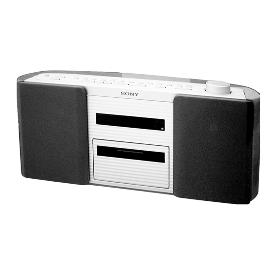
Sony ZS-2000 Service Manual
Personal audio system
Hide thumbs
Also See for ZS-2000:
- Operating instructions manual (36 pages) ,
- Service manual (58 pages)
Table of Contents
Advertisement
Quick Links
SERVICE MANUAL
Ver 1.0 2000. 04
CD player section
System
Compact disc digital audio system
Laser diode properties
Material: GaAlAs
Wave length: 780 nm
Emission duration: Continuous
Laser output: Less than 44.6 µW
(This output is the value measured at a distance of
about 200 mm from the objective lens surface on
the optical pick-up block with 7 mm aperture.)
Spindle speed
200 r/min (rpm) to 500 r/min (rpm) (CLV)
Number of channels
2
Frequency response
20 - 20,000 Hz +0.5/–0.7 dB
Wow and flutter
Below measurable limit
Radio section
Frequency range
FM: 87.5 - 108 MHz
MW: 531 - 1,602 kHz
LW: 153 - 279 kHz
IF
FM: 10.7 MHz
MW/LW: 450 kHz
Aerials
FM: Telescopic aerial
MW/LW: Loop aerial
Radio-controlled clock: Ferrite-bar aerial
ZS-2000
Model Name Using Similar Mechanism ZS-D50
CD Loading Mechanism Type
CD
Section CD Mechanism Type
Optical Pick-up Name
SPECIFICATIONS
General
Speaker
Full range: 8 cm (3
Input
LINE IN jack (stereo minijack)
Minimum input level 250 mV
Outputs
Headphones jack (stereo minijack)
For 16 - 68 ohms impedance headphones
OPTICAL DIGITAL OUT (CD) (optical output
connector)
Wavelength: 630 - 690 nm
Maximum power output
7.5 W + 7.5 W
Power requirements
For personal audio system:
230 V AC, 50 Hz
For remote control:
3 V DC, 2 R6 (size AA) batteries
Power consumption
AC 28 W
Dimensions (incl. projecting parts)
approx. 470 × 206.5 × 145.5 mm (w/h/d)
× 8
× 5
(18
5
/
1
/
8
4
Mass
approx. 5 kg (11 lb.)
Supplied accessories
Remote control (1) (RMT-C200AD)
Aerial unit (1)
Speaker nets (2)
Design and specifications are subject to change without
notice.
PERSONAL AUDIO SYSTEM
– 1 –
AEP Model
VLM-ZS2000
CDM-2411AAA
DAX-01A2
1
/
in.) dia., 4 ohms, cone type x 2
4
3
/
inches)
4
Advertisement
Table of Contents

Related Manuals for Sony ZS-2000


Summary of Contents for Sony ZS-2000
- Page 1 ZS-2000 SERVICE MANUAL AEP Model Ver 1.0 2000. 04 Model Name Using Similar Mechanism ZS-D50 CD Loading Mechanism Type VLM-ZS2000 Section CD Mechanism Type CDM-2411AAA Optical Pick-up Name DAX-01A2 SPECIFICATIONS CD player section General System Speaker Compact disc digital audio system Full range: 8 cm (3 in.) dia., 4 ohms, cone type x 2...
-
Page 2: Table Of Contents
TABLE OF CONTENTS 1. SERVICING NOTES 5. ELECTRICAL ADJUSTMENTS 1-1. Notes on Handling the Optical Pick-up Block or Base Unit .. 3 5-1. Tuner Section ..............19 1-2. Notes on Laser Diode Emission Check ....... 3 5-2. Loop Antenna Section ............21 1-3. -
Page 3: Servicing Notes
COMPONENTS IDENTIFIED BY MARK 0 OR DOTTED LINE WITH MARK 0 ON THE SCHEMATIC DIAGRAMS AND IN THE PARTS LIST ARE CRITICAL TO SAFE OPERATION. REPLACE THESE COMPONENTS WITH SONY PARTS WHOSE PART NUMBERS APPEAR AS SHOWN IN THIS MANUAL OR IN SUPPLEMENTS PUBLISHED BY SONY. -
Page 4: General
SECTION 2 GENERAL This section is extracted from instruction manual. Basic Operations Setting the clock automatically Tips If the player fails to receive the clock data signal This player is equipped with the Radio-Controlled Clock Auto Adjust System. The • You can use this player for 12 minutes system receives clock data (hour, minute, second, and adjustment to/from daylight before you set the clock. -
Page 5: Listening To The Radio
Listening to the radio Use these buttons for additional operations PLAY MODE OPERATE MONO/ST VOLUME Do this adjust the volume Turn VOLUME toward + or – (press VOL +, – on the remote). Connect the mains lead to the mains (see page 35). turn on/off the radio Press OPERATE. -
Page 6: Preparing The System
Setting Up Preparing the Tips system Aerial terminals 2 Connecting the mains lead • The sound quality may Connect the mains lead to the mains. be changed depending on the polarity of the According to the illustrations, mains plug. Change the connect the cords firmly. -
Page 7: Disassembly
SECTION 3 DISASSEMBLY Note : This set can be disassemble according to the following sequence. “Net Sub Assy, Saran”, Speaker (Front) Sub Assy Cabinet, Front Power Board, CD Block Assy REG Board Top Cabinet Assy TU Board, EXT ANT Board “Cover, Heat Sink”, Line Board Volume Board FL Board, Lamp Board... -
Page 8: Cabinet, Front
• Note for installation of the speaker (front) sub assy There are two types of net “bush, net”: Type-A: 3-041-456-11 (with groove in the tube) Type-B: 3-041-456-01 (without groove in the tube) The type A of “bush, net” should be installed at place A in the left figure. The type B of “bush, net”... -
Page 9: Top Cabinet Assy
3-3. TOP CABINET ASSY 5 antenna, telescopic 8 top cabinet assy 7 BVTP 3x10 3 P7 2 CN804 1 CN904 6 BVTP 3x10 4 B 3x10 3-4. CD BLOCK ASSY 1 CN903 2 CN902 0 CN402 5 RETAINER (2) board 4 BVTP 3x10 qa CN403 qs CNP1... -
Page 10: Power Board, Reg Board
3-5. POWER BOARD, REG BOARD 4 POWER board 3 BVTP 3x10 1 CN901 2 BVTP 3x10 6 REG board 5 BVTP 3x10 3-6. TU BOARD, EXT ANT BOARD 1 BVTP 2.6x10 7 B 3x6 5 EXT ANT board 4 B 3x6 6 Removal the solder. -
Page 11: Cover, Heat Sink", Line Board
3-7. “COVER, HEAT SINK”, LINE BOARD 5 claws 4 claws 8 holder, line 7 BVTP 3x10 3 claws 6 cover, heat sink 9 BVTP 3x10 0 LINE board 2 BVTP 3x10 1 BVTP 3x10 3-8. VOLUME BOARD 3 BVTP 3x10 2 CN806 5 VOLUME board 4 claws... -
Page 12: H/P Board, Switch (1) Board, Switch (2) Board
3-9. H/P BOARD, SWITCH (1) BOARD, SWITCH (2) BOARD 7 BVTP 3x8 9 SWITCH (1) board 6 BVTP 3x8 4 BVTP 3x8 5 SWITCH (2) board 3 CN805 1 PWH 2x8 (DIA.6) 2 H/P board 3-10. FL BOARD, LAMP BOARD 2 CN501 1 CN502 claws... -
Page 13: Control Board
3-11. CONTROL BOARD 3 BVTP 3x10 4 CONTROL board 2 CN801 1 CN802 3-12. MAIN BOARD 5 MAIN board 3 BVTP 3x10 2 BVTP 3x10 1 CN303 claws – 13 –... -
Page 14: Cd Board
3-13. CD BOARD 2 BVTP 3x10 1 CN711 4 CD board 5 CN713 3-14. CD BLOCK SECTION 3 CD block section 1 BVTP 3x10 chassis, CD 2 BVTP 3x10 – 14 –... -
Page 15: Tray Assy, Cd
3-15. TRAY ASSY, CD 3 Screws 9 Screws (+BV 3X10) (+BV 3X10) 0 Plate (L), Side Loading chassis 7 Plate (R), Side 4 Cover (L), Side 8 Slider (L) 1 Screws (+BV 3X10) qa CD lid assy 5 Slider (R) qf tray assy, CD 6 Screws (+BV 3X10) -
Page 16: Optical Pick-Up, Pick-Up Relay Board
3-17. OPTICAL PICK-UP, PICK-UP RELAY BOARD 3 tray (top), CD qa CN703 qs optical pick-up block 0 CN704 9 CN702 7 CN707 5 claw 6 PICK-UP RELAY board 8 CN706 4 claw tray (bottom), CD 1 BTP 2.6x8 2 BTP 2.6x8 3-18. -
Page 17: Test Mode
SECTION 4 TEST MODE – SWITCH (1) BOARD – 4-1. GENERAL DESCRIPTION This set has the TEST MODE that allows the CD unit to be operational checked. RADIO/BAND AUTO PRESET TEST-A 4-2. TEST MODE 4-2-1. Setting the test mode CLOCK TIMER Short the TEST-A land on the SWITCH(1) BOARD to open it (or short between JW824 and JW825 to open the circuit). - Page 18 4-2-4. MODE transition table KEY operated TUNE TUNE TIME SET – TIME SET + STOP PLAY/PAUSE Current TEST MODE While held down When released While held down When released STOP 1 STOP 1 FOCUS SLED RWD STOP 1 SLED FWD STOP 1 STOP 2 STOP 1...
-
Page 19: Electrical Adjustments
SECTION 5 ELECTRICAL ADJUSTMENTS 5-1. TUNER SECTION 0 dB = 1 µV FM FREQUENCY COVERAGE CHECK Precautions in Repairing Note : As a tuner unit (TU1) is difficult to repair if faulty, Frequency Display 87.5 MHz 108 MHz replace it with new one. Reading on Digital voltmeter 1.4 ±... - Page 20 Adjustment Location: (COMPONENT SIDE) TRACKING ADJUSTMENT LW FREQUENCY COVERAGE ADJUSTMENT TP(VT) TRACKING ADJUSTMENT AM FREQUENCY COVERAGE ADJUSTMENT AM IF ADJUSTMENT – 20 –...
-
Page 21: Loop Antenna Section
5-2. LOOP ANTENNA SECTION Antenna Adjustment Setting: AM RF signal oscilloscope generator (DC range) Put the lead-wire antenna close to CL/RECEIVER board the supplied TP601 loop antenna. TP602 77.5 kHz frequency Probe no modulation 10:1 10MΩ Procedure: 1. Connect the oscilloscope between TP601 and TP602 on the CL/RECEIVER board. -
Page 22: Diagrams
SECTION 6 DIAGRAMS 6-1. IC PIN DESCRIPTION • IC801 CXP84332-222Q (SYSTEM CONTROL) Pin No. Pin Name Pin Description R-COUNT PLL IC count data output R-CE PLL IC chip enable output. R-CLK PLL IC clock output. R-DATA PLL IC data output. R-MUTE Tuner mute signal output. - Page 23 Pin No. Pin Name Pin Description SIRCS remote control signal input from the remote control receiver (IC602) — Not used C-DATA Serial data output to the CD DSP IC (IC702) C-XLAT Serial data latch pulse signal output to the CD DSP IC (IC702) C-XRST Reset signal output to the CD RF AMP (IC701), CD DSP IC (IC702) C-SCOR...
-
Page 24: Circuit Boards Location
6-2. CIRCUIT BOARDS LOCATION H/P board SWITCH (2) board SWITCH (1) board EXT ANT SWITCH board VOLUME board CL/RECEIVER board SPK (R) board POWER board SPK (L) board REG board RETAINER (2) board LINE board TU board CONTROL board FL board LAMP board MAIN board LOADING board... -
Page 25: Block Diagram -Tuner Section
ZS-2000 6-3. BLOCK DIAGRAM — TUNER SECTION — ANT2 MAIN MW/LW (Page 29) BOARD(2/2) CN302 LOOP ANTENNA C/T TCO CL/RECEIVER BOARD TU BOARD MAIN BOARD CONTROL BOARD (1/3) CT1,L3 CT2,L4 AM FRONT-END (1/2) FM/AM IF,DET,MPX 2.5V TRACKING TRACKING L601 POWER... -
Page 26: Block Diagram -Cd Section
ZS-2000 6-4. BLOCK DIAGRAM — CD SECTION — PICK-UP CD BOARD OPTICAL CN704 RELAY CD RF & SYSTEM SERVO PROCESSOR DSP & D/A CONV. PICK-UP BLOCK BOARD IC701 IC702 (DAX-01A2) MO6V MO6V MAIN BOARD CD 5V CD 5V CN706 CN711... -
Page 27: Block Diagram -Audio Section
ZS-2000 6-5. BLOCK DIAGRAM — AUDIO SECTION — MAIN BOARD (2/2) SPK(R) BOARD LINE BOARD (1/2) SP302 R-CH R-CH J402 SPEAKER CN402 CNP302 LINE IN CN304 LINE LCH ELECTRONIC VOLUME IC301 POWER AMP SPK(L) BOARD IC303 LINE TU L CH... -
Page 28: Printed Wiring Boards -Tuner Section
ZS-2000 6-6. PRINTED WIRING BOARDS — TUNER SECTION — • Refer to page 24 for Circuit Boards Location. J1-2 J1-1 FM EXT MW/LW ANTENNA ANTENNA ANT1 FM TELESCOPIC EXT ANT ANTENNA SWITCH BOARD TU BOARD MAIN BOARD CN302 (Page 44) -
Page 29: Schematic Diagrams -Tuner Section
ZS-2000 6-7. SCHEMATIC DIAGRAMS — TUNER SECTION — • Refer to page 61 for IC Block Diagrams. • Refer to page 31 for Note. (Page 45) EXT ANT SWITCH BOARD (Page 45) Note on Schematic Diagram: • Voltage is dc with respect to ground under no-signal (detuned) condition. -
Page 30: Printed Wiring Boards -Cd Section
ZS-2000 6-8. PRINTED WIRING BOARDS — CD SECTION — • Refer to page 24 for Circuit Boards Location. • Refer to page 31 for Note. • Waveforms (MODE:PLAY) 0.1V/div 20µsec/div (Page 44) MAIN BOARD CN303 2.5V Approx. 150mVp-p CD BOARD... -
Page 31: Schematic Diagrams -Cd Section
ZS-2000 6-9. SCHEMATIC DIAGRAMS — CD SECTION — • Refer to page 62 for IC Block Diagrams. • Refer to page 31 for Note. (Page 41) (Page 41) Note on Schematic Diagram: (Page 45) • Voltage and waveforms are dc with respect to ground under no-signal (detuned) conditions. -
Page 32: Printed Wiring Boards -Pick-Up Section
ZS-2000 6-10. PRINTED WIRING BOARDS — PICK-UP SECTION — • Refer to page 24 for Circuit Boards Location. • Refer to page 31 for Note. CD BOARD (Page 35) CN711 PICK-UP CN702 CN704 CN703 RELAY BOARD M802 (SPINDLE) OPTICAL PICK-UP BLOCK... -
Page 33: Schematic Diagrams -Pick-Up Section
ZS-2000 6-11. SCHEMATIC DIAGRAMS — PICK-UP SECTION — • Refer to page 61 for IC Block Diagrams. • Refer to page 31 for Note. (Page 38) (Page 38) Note on Schematic Diagram: • Voltage is dc with respect to ground under no-signal (detuned) condition. - Page 34 ZS-2000 6-12. PRINTED WIRING BOARDS — MAIN SECTION — • Refer to page 24 for Circuit Boards Location. • Refer to page 31 for Note. (Page 47) CONTROL BOARD CN801 • Semiconductor Location Ref. No. Location Ref. No. Location MIAN BOARD...
-
Page 35: Schematic Diagrams -Main Section
ZS-2000 6-13. SCHEMATIC DIAGRAMS — MAIN SECTION — • Refer to page 64 for IC Block Diagrams. • Refer to page 31 for Note. SP302 R-CH SPEAKER SP301 L-CH SPEAKER (Page 57) (Page 49) (Page 57) (Page 38) (Page 34) - Page 36 ZS-2000 6-14. PRINTED WIRING BOARDS — CONTROL SECTION — • Refer to page 64 for Circuit Boards Location. • Refer to page 31 for Note. PRESET SWITCH(1) BOARD RADIO/BAND SNOOZE (TEST-A) > + AUTO PRESET OPEN/CLOSE SUMMER CLOCK TUNE DISPLAY...
-
Page 37: Schematic Diagrams -Control Section
ZS-2000 6-15. SCHEMATIC DIAGRAMS — CONTROL SECTION — • Refer to page 64 for IC Block Diagrams. • Refer to page 31 for Note. (Page 37) Note on Schematic Diagram: • Voltage is dc with respect to ground under no-signal (detuned) condition. -
Page 38: Printed Wiring Boards -Display Section
ZS-2000 6-16. PRINTED WIRING BOARDS — DISPLAY SECTION — • Refer to page 24 for Circuit Boards Location. • Refer to page 31 for Note. (Page 47) (Page 43) CONTROL BOARD MAIN BOARD CN803 CNP307 FL BOARD FL501 FLUORESCENT INDICATOR TUBE... -
Page 39: Schematic Diagrams -Display Section
ZS-2000 6-17. SCHEMATIC DIAGRAMS — DISPLAY SECTION — • Refer to page 31 for Note. Note on Schematic Diagram: • Voltage is dc with respect to ground under no-signal (detuned) condition. no mark : FM (Page 45) (Page 49) – 53 –... - Page 40 ZS-2000 6-18. PRINTED WIRING BOARDS — POWER SUPPLY SECTION — • Refer to page 24 for Circuit Boards Location. • Refer to page 31 for Note. H/P BOARD POWER BOARD • Semiconductor Location AC IN Ref. No. Location D901 D902...
-
Page 41: Schematic Diagrams -Power Supply Section
6-19. SCHEMATIC DIAGRAMS — POWER SUPPLY SECTION — • Refer to page 31 for Note. (Page 46) : NOT REPLACEABLE, BUILT IN TRANSFORMER. (Page 46) (Page 46) Note on Schematic Diagram: • Voltage is dc with respect to ground under no-signal (detuned) condition. -
Page 42: Printed Wiring Board -Loop Antenna Section
6-20. PRINTED WIRING BOARD — LOOP ANTENNA SECTION — • Refer to page 24 for Circuit Boards Location. • Refer to page 31 for Note. CL/RECEIVER BOARD L601 RADIO-CONTROLLED CLOCK FERRITE-ROD ANTENNA TP602 TP601 : Solder bridge ANT2 MW/LW LOOP ANTENNA TU BOARD J1-1... -
Page 43: Schematic Diagram -Loop Antenna Section
ZS-2000 6-21. SCHEMATIC DIAGRAM — LOOP ANTENNA SECTION — • Refer to page 64 for IC Block Diagrams. • Refer to page 31 for Note. TU BOARD J1-1 TERMINAL MW/LW ANTENNA Note on Schematic Diagram: • Voltage is dc with respect to ground under no-signal (detuned) condition. - Page 44 • IC BLOCK DIAGRAM IC1 LA1833N IC701 CXA1992BR PILOT OSC IN RF IN DET OUT DET OUT 32 31 28 27 RF. AMP BUFF DECODER PILOT ANTI-BIRDIE CANCEL RF SUMMING AMP PD2 IV PD1 IV 26 SENS2 P-DET STEREO FE BIAS Ø...
- Page 45 IC703 CXD2589Q 59 58 57 54 53 52 51 SYSM SERIAL-IN INTERFACE LRCKI LRCK AVSS OVER SAMPLING ASYO DIGITAL FILTER ASYI ASYMMETRY DEMODULATOR CORRECTOR AVDD BIAS 3rd-ORDER AVDD NOISE SHAPER AOUT1 AIN1 CLTV LOUT1 AVSS ERROR XVDD CORRECTOR AVSS XTAI SUB CODE PROCESSOR DIGITAL...
- Page 46 IC301 BD3859AFV 40 39 30 29 25 24 DYNAMIC DYNAMIC TREBLE1 TREBLE2 BASS 2 BASS 1 BASS1 BASS2 31dB VCC/2 VCC/2 VCC2 VCC/2 VCC/2 VCC/2 VCC/2 VCC2 LOGIC 14 15 IC804 MSM9805-549RS 18 BIT 2M BIT ADDRESS MULTIPLEXER CONTROLLER 18 BIT DATA ADDRESS CONTROLLER...
-
Page 47: Exploded Views
SECTION 7 EXPLODED VIEWS NOTE: • The mechanical parts with no reference • Color Indication of Appearance Parts The components identified by mark 0 or dotted line with mark number in the exploded views are not supplied. Example : 0 are critical for safety. •... -
Page 48: Rear Cabinet Section
7-2. REAR CABINET SECTION ANT1 F901 not supplied T901 not supplied The components identified by mark 0 or dotted line with mark 0 are critical for safety. Replace only with part number specified. Ref. No. Part No. Description Remark Ref. No. Part No. -
Page 49: Cd Block Section
7-3. CD BLOCK SECTION not supplied FL501 not supplied Ref. No. Part No. Description Remark Ref. No. Part No. Description Remark * 101 A-3323-477-A FL BOARD, COMPLETE 1-792-175-11 WIRE (FLAT TYPE) (FFC) (13 CORE) * 102 1-676-090-11 LAMP BOARD 1-792-513-11 WIRE, PARALLEL (22 CORE) 3-041-440-01 HOLDER, FLT * 109 A-3322-573-A MAIN BOARD, COMPLETE... -
Page 50: Cd Loading Section (Vlm-Zs2000)
7-4. CD LOADING SECTION (VLM-ZS2000) M790 CDM-2411AAA Ref. No. Part No. Description Remark Ref. No. Part No. Description Remark 3-017-025-11 COVER (R), SIDE * 167 1-667-045-11 LOADING BOARD 3-017-012-11 PLATE (R), SIDE 3-017-031-11 GEAR (A) 3-017-014-11 SLIDER (R) 3-017-032-11 GEAR (B) 3-017-027-11 GEAR (C) 3-017-030-01 BELT 3-017-016-11 SHAFT, TRAY... -
Page 51: Optical Pick-Up Section (Cdm-2411Aa)
7-5. OPTICAL PICK-UP SECTION (CDM-2411AA) M802 M801 S891 The components identified by mark 0 or dotted line with mark 0 are critical for safety. Replace only with part number specified. Ref. No. Part No. Description Remark Ref. No. Part No. Description Remark A-3303-970-A SCREW ASSY, FEED... -
Page 52: Loop Antenna Section
7-6. LOOP ANTENNA SECTION Ref. No. Part No. Description Remark Ref. No. Part No. Description Remark X-3379-075-1 ANTENNA ASSY, LOOP (including ANT2) 3-048-153-01 CASE, LOOP (FRONT) 3-048-156-01 SCREW (+PWH) (2.6X10) * 256 A-3323-472-A CL/RECEIVER BOARD, COMPLETE 3-048-155-01 STOPPER, LOOP 3-048-154-01 CASE, LOOP (REAR) 3-048-341-01 FELT –... -
Page 53: Electrical Parts List
SECTION 8 ELECTRICAL PARTS LIST NOTE: • Due to standardization, replacements in • Items marked “*” are not stocked since The components identified by the parts list may be different from the they are seldom required for routine service. mark 0 or dotted line with mark parts specified in the diagrams or the Some delay should be anticipated 0 are critical for safety. - Page 54 CL/RECEIVER Ref. No. Part No. Description Remark Ref. No. Part No. Description Remark L704 1-414-402-11 INDUCTOR 47uH R748 1-216-105-11 RES-CHIP 220K 1/10W R749 1-216-041-00 METAL CHIP 1/10W < TRANSISTOR > R750 1-216-049-11 RES-CHIP 1/10W R751 1-216-049-11 RES-CHIP 1/10W Q701 8-729-101-07 TRANSISTOR 2SB798-DL R752 1-216-105-11 RES-CHIP 220K...
- Page 55 CL/RECEIVER CONTROL Ref. No. Part No. Description Remark Ref. No. Part No. Description Remark R608 1-249-431-11 CARBON 1/4W C895 1-102-518-11 CERAMIC 33PF C896 1-126-924-11 ELECT 330uF < VIBRATOR > C897 1-162-306-11 CERAMIC 0.01uF C898 1-162-306-11 CERAMIC 0.01uF X601 1-767-219-11 FILTER, CRYSTAL (77.5kHz) <...
- Page 56 CONTROL EXT ANT SWITCH Ref. No. Part No. Description Remark Ref. No. Part No. Description Remark R823 1-249-437-11 CARBON 1/4W R893 1-249-410-11 CARBON 1/4W R824 1-249-437-11 CARBON 1/4W R895 1-249-425-11 CARBON 4.7K 1/4W R825 1-249-437-11 CARBON 1/4W R897 1-247-807-31 CARBON 1/4W R826 1-249-429-11 CARBON...
- Page 57 LAMP LINE LOADING Ref. No. Part No. Description Remark Ref. No. Part No. Description Remark IC502 8-759-459-85 IC NJL63H400A 1-677-452-11 LINE BOARD *********** < JUMPER RESISTOR > < CAPACITOR > JR501 1-216-296-00 SHORT JR502 1-216-296-00 SHORT C401 1-162-851-11 CERAMIC 0.1uF JR503 1-216-296-00 SHORT C402...
- Page 58 LOADING MAIN Ref. No. Part No. Description Remark Ref. No. Part No. Description Remark < SWITCH > C217 1-136-165-00 MYLAR 0.1uF C218 1-136-165-00 MYLAR 0.1uF S790 1-762-951-11 SWITCH, PUSH (CLOSE) C219 1-162-286-21 CERAMIC 220PF S791 1-762-951-11 SWITCH, PUSH (OPEN) C220 1-162-282-31 CERAMIC 100PF C221...
- Page 59 MAIN Ref. No. Part No. Description Remark Ref. No. Part No. Description Remark D305 8-719-991-33 DIODE 1SS133T-77 R119 1-249-435-11 CARBON 1/4W D306 8-719-991-33 DIODE 1SS133T-77 R120 1-249-441-11 CARBON 100K 1/4W D350 8-719-982-28 DIODE MTZJ-33D R121 1-249-424-11 CARBON 3.9K 1/4W D351 8-719-921-54 DIODE MTZJ-6.2B R122 1-247-881-00 CARBON...
- Page 60 MAIN PICK-UP RELAY POWER SPK (L) SPK (R) SWITCH (1) Ref. No. Part No. Description Remark Ref. No. Part No. Description Remark R358 1-247-895-11 CARBON 470K 1/4W D913 8-719-063-79 DIODE 10E2 R359 1-249-441-11 CARBON 100K 1/4W R360 1-247-895-11 CARBON 470K 1/4W <...
- Page 61 SWITCH (1) SWITCH (2) Ref. No. Part No. Description Remark Ref. No. Part No. Description Remark R873 1-249-418-11 CARBON 1.2K 1/4W 1-163-021-11 CERAMIC CHIP 0.01uF R892 1-249-420-11 CARBON 1.8K 1/4W 1-163-021-11 CERAMIC CHIP 0.01uF R894 1-247-843-11 CARBON 3.3K 1/4W 1-163-021-11 CERAMIC CHIP 0.01uF 1-163-109-11 CERAMIC CHIP 47PF...
- Page 62 Ref. No. Part No. Description Remark Ref. No. Part No. Description Remark 1-163-117-11 CERAMIC CHIP 100PF JR15 1-216-295-00 SHORT 1-163-117-11 CERAMIC CHIP 100PF JR16 1-216-295-00 SHORT 1-163-117-11 CERAMIC CHIP 100PF JR17 1-216-295-00 SHORT 1-163-117-11 CERAMIC CHIP 100PF JR18 1-216-295-00 SHORT 1-163-021-11 CERAMIC CHIP 0.01uF JR19...
- Page 63 VOLUME Ref. No. Part No. Description Remark Ref. No. Part No. Description Remark 1-216-033-00 METAL CHIP 1/10W MISCELLANEOUS 1-216-049-11 RES-CHIP 1/10W *************** 1-216-065-11 RES-CHIP 4.7K 1/10W 0 69 1-216-073-00 METAL CHIP 1/10W 1-696-169-21 CORD, POWER 1-216-049-11 RES-CHIP 1/10W 1-792-686-11 WIRE, PARALLEL (FFC) (8 CORE) 1-792-175-11 WIRE (FLAT TYPE) (FFC) (13 CORE) 1-216-105-11 RES-CHIP 220K...
- Page 64 ZS-2000 Sony Corporation 2000D0444-1 9-927-686-11 Personal Audio Division Company Printed in Japan C2000. 4 – 82 – Published by General Engineering Dept.