Advertisement
Quick Links
ORDER NO.MKE0309803C1
B3
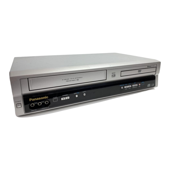
DVD VIDEO PLAYER/ VIDEO CASSETTE REOCRDER
PV-D734S / PV-D744S
ORIGINAL MFR'S VERSION A
1. CAUTION
THIS DIGITAL VIDEO PLAYER EMPLOYS A LASER SYSTEM.
TO ENSURE PROPER USE OF THIS PRODUCT, PLEASE READ THIS SERVICE MANUAL CARE-
FULLY AND RETAIN FOR FUTURE REFERENCE. SHOULD THE UNIT REQUIRE MAINTENANCE,
CONTACT AN AUTHORIZED SERVICE LOCATION-SEE SERVICE PROCEDURE.
USE OF CONTROLS, ADJUSTMENTS OR THE PERFORMANCE OF PROCEDURES OTHER THAN
THOSE SPECIFIED HEREIN MAY RESULT IN HAZARDOUS RADIATION EXPOSURE.
TO PREVENT DIRECT EXPOSURE TO LASER BEAM, DO NOT TRY TO OPEN THE ENCLOSURE.
VISIBLE LASER RADIATION MAY BE PRESENT WHEN THE ENCLOSURE IS OPENED. DO NOT
STARE INTO BEAM.
1
Advertisement

Related Manuals for Panasonic PV-D734S


Summary of Contents for Panasonic PV-D734S
- Page 1 ORDER NO.MKE0309803C1 DVD VIDEO PLAYER/ VIDEO CASSETTE REOCRDER PV-D734S / PV-D744S ORIGINAL MFR'S VERSION A 1. CAUTION THIS DIGITAL VIDEO PLAYER EMPLOYS A LASER SYSTEM. TO ENSURE PROPER USE OF THIS PRODUCT, PLEASE READ THIS SERVICE MANUAL CARE- FULLY AND RETAIN FOR FUTURE REFERENCE. SHOULD THE UNIT REQUIRE MAINTENANCE, CONTACT AN AUTHORIZED SERVICE LOCATION-SEE SERVICE PROCEDURE.
- Page 2 2. IMPORTANT SERVICE SAFETY INFORMATION Operating the receiver outside of its cabinet or with its back removed involves a shock hazard. Work on these models should only be performed by those who are thoroughly familiar with precautions necessary when working on high voltage equipment. Exercise care when servicing this chassis with power applied.
- Page 3 When removing springs or spring mounted parts from the tuner, tuner cluster or chassis, shatterproof goggles must be worn. Keep others without shatterproof goggles away. Before returning the receiver to the user, perform the following safety checks: 1. Inspect all lead dress to make certain that leads are not pinched or that hardware is not lodged between the chassis and other metal parts in the receiver.
- Page 4 2. Remove the screw 1 of the Deck Chassis and remove the Loading Motor. (Refer to Fig. 2 3. Rotate the Pinch Roller Cam in the direction of the arrow by hand to slacken the Video Tape. 4. Rotate the Clutch Ass'y either of the derections to wind the Video Tape in the Cassette Case.
- Page 5 6. PARENTAL CONTROL - RATING LEVEL 4 DIGIT PASSWORD CANCELLATION If the stored 4 digit password in the Rating Level menu needs to be cancelled, please follow the steps below. 1. Turn Unit ON. 2. Press and hold the '7' key on the remote control unit. 3.
- Page 6 Caution: - Pb free solder has a higher melting point than standard solder; Typically the melting point is 50°F~70°F (30°C~40°C) higher. Please use a soldering iron with temperature control and adjust it to 700°F ± 20°F (370°C ± 10°C). In case of using high temperature soldering iron, please be carefull not to heat too long.
- Page 7 6. Remove the 2 screws 7. Remove the Operation PCB in the direction of arrow (C). Fig. 1-1 9.1.2. FLAP (Refer to Fig. 1-2 1. Open Flap to 90° and flex in direction of arrow (A), at the same time slide in direction of arrow (B). 2.
- Page 8 5. Disconnect the following connectors: (CP2601, CP2602, CP2603). 6. Remove the DVD Deck in the direction of arrow (B). 7. Remove the 3 screws 8. Remove the Front Angle in the direction of arrow (C). 9. Remove the screw 10. Remove the DVD Angle. Fig.
- Page 9 9.1.5. VCR DECK (Refer to Fig. 1-5 NOTE Do not remove the cable at the FE Head section. The FE Head may be damaged if you remove the cable by force. 1. Move the Cassette Holder Ass’y to the back side. 2.
- Page 10 2. Remove the 2 screws 3. Remove the screw 4. Remove the 3 Pin Shield. 5. Remove the VCR PCB in the direction of arrow. Fig. 1-6 9.2. REMOVAL OF VCR DECK PARTS 9.2.1. TOP BRACKET (Refer to Fig. 2-1 1.
- Page 11 2. Push the Locker R to remove the Cassette Side R. 3. Remove the Cassette Side L. Fig. 2-2 9.2.3. CASSETTE SIDE L/R (Refer to Fig. 2-3-A 1. Remove the Locker Spring. 2. Unlock the 4 supports and then remove the Cassette Side L/R. 3.
- Page 12 9.2.4. LINK UNIT (Refer to Fig. 2-4 1. Set the Link Unit to the Eject position. 2. Unlock the support 3. Remove the (A) side of the Link Unit first, then remove the (B) side. Fig. 2-4 9.2.5. LINK LEVER/FLAP LEVER (Refer to Fig.
- Page 13 3. Remove the Worm. Fig. 2-6-A NOTE 1. In case of the Worm installation, check if the value of the Fig. 2-6-B is correct. 2. In case of the Loading Motor installation, hook the wire on the Cassette Opener as shown Fig.
- Page 14 9.2.7. TENSION ASS'Y (Refer to Fig. 2-7-B 1. Turn the Pinch Roller Cam clockwise so that the Tension Holder hook is set to the position of Fig. 2-7-A to move the Tension Arm Ass'y. 2. Remove the Tension Spring. 3. Unlock the 2 supports and remove the Tension Band.
- Page 15 Fig. 2-7-C Fig. 2-7-D Fig. 2-7-E 9.2.8. T BRAKE ARM/T BRAKE BAND (Refer to Fig. 2-8-A 1. Remove the T Brake Spring. 2. Turn the T Brake Arm clockwise and bend the hook section to remove it. 3. Unlock the 2 supports and remove the T Brake Band.
- Page 16 9.2.9. S REEL/T REEL/IDLER ARM ASS'Y/IDLER GEAR (Refer to Fig. 2-9-A 1. Remove the S Reel and T Reel. 2. Remove the 2 Polyslider Washers 3. Remove the Idler Arm Ass'y and Idler Gear. NOTE 1. Take care not to damage the gears of the S Reel and T Reel. 2.
- Page 17 1. In case of the S Reel and T Reel installation, check if the correct parts are installed. (Refer to Fig. 2-9-B 2. In case of the Idler Arm Ass'y installation, install correctly as Fig. 2- . And also set it so that the section "B" of Fig.
- Page 18 Fig. 2-10-B 9.2.11. A/C HEAD (Refer to Fig. 2-11-A 1. Remove the screw 2. Remove the A/C Head Base. 3. Remove the 3 screws 4. Remove the A/C Head and A/C Head Spring. NOTE 1. Do not touch the A/C Head. (Use gloves.) 2.
- Page 19 9.2.12. FE HEAD (RECORDER ONLY) (Refer to Fig. 2-12 1. Remove the screw 2. Remove the FE Head. Fig. 2-12 9.2.13. AHC ASS'Y/CYLINDER UNIT ASS'Y (Refer to Fig. 2-13 1. Unlock the support and remove the AHC Ass'y. 2. Disconnect the following connector: (CD2001) 3.
- Page 20 1. Remove the Capstan Belt. 2. Remove the 3 screws 3. Remove the Capstan DD Unit. Fig. 2-14-A NOTE 1. In case of the Capstan DD Unit installation, apply the silicon bond (TSE3843-W) on the position Fig. 2-14-B correctly. (If no silicon bond applied, abnormal noise will be heard on the deck operation.) (Referto Fig.
- Page 21 1. Remove the E-Ring , then remove the Main Cam. 2. Remove the E-Ring , then remove the Pinch Roller Cam and Joint Gear. Fig. 2-15-A NOTE 1. In case of the Pinch Roller Cam and Main Cam installation, install them as the circled section of Fig.
- Page 22 NOTE 1. When you install the Loading Arm S Unit, Loading Arm T Unit and Main Loading Gear, align each marker. (Refer to Fig. 2-16-B Fig. 2-16-B 9.2.17. CLUTCH ASS'Y/RING SPRING/CLUTCH LEVER/ CLUTCH GEAR (Refer to Fig. 2-17-A 1. Remove the Polyslider Washer 2.
- Page 23 NOTE 1. In case of the Clutch Ass'y installation, install it with inserting the spring of the Clutch Ass'y into the dent of the Coupling Gear. (Refer to Fig. 2-17-B Fig. 2-17-B 9.2.18. CASSETTE GUIDE POST/INCLINED BASE S/T UNIT/P4 CAP/LED REFLECTOR (Refer to Fig.
- Page 24 NOTE 1. Do not touch the roller of Guide Roller. 2. In case of the P4 Cap installation, install it with parallel for "A" and "B" of Fig. 2-18-B 3. In case of the Cassette Guide Post installation, install correctly as the circled section of Fig.
- Page 25 REMOVAL 1. Put the Masking Tape (cotton tape) around the Flat Package IC to protect other parts from any damage. (Refer to Fig. 3-1 NOTE Masking is carried out on all the parts located within 10 mm distance from IC leads. Fig.
- Page 26 Some ICs on the PCB are affixed with glue, so be careful not to break or damage the foil of each IC leads or solder lands under the IC when removing it. Fig. 3-3 4. Peel off the Masking Tape. 4. 5.
- Page 27 2. Supply the solder from the upper position of IC leads sliding to the lower position of the IC leads. (Refer to Fig. 3-6 Fig. 3-6 3. Absorb the solder left on the lead using the Braided Shield Wire. (Refer to Fig.
- Page 28 5. Finally, confirm the soldering status on four sides of the IC using a magnifying glass. Confirm that no abnormality is found on the soldering position and installation position of the parts around the IC. If some abnormality is found, correct by resoldering. NOTE When the IC leads are bent during soldering and/or repairing, do not repair the bending of leads.
- Page 29 12. PREVENTIVE CHECKS AND SERVICE INTERVALS The following standard table depends on environmental conditions and usage. Parts replacing time does not mean the life span for individual parts. Also, long term storage or misuse may cause transformation and aging of rubber parts. The following list means standard hours, so the checking hours depends on the conditions.
- Page 30 Total hours are displayed in 16 system of notation. NOTE: If you set a factory initialization, the total hours is reset to "0". 1. Connect the set to TV Monitor. 2. Turn on the POWER. 3. Press both CH UP button on the set and the FF button on the set for more than 2 seconds.
- Page 31 2. TAPE RUNNING SYSTEM When cleaning the tape transport system, use the gauze moistened with isopropyl alcohol. 3. CYLINDER Wrap a piece of chamois around your finger. Dip it in isopropyl alcohol. Hold it to the cylinder head softly. Turn the cylinder head counterclockwise to clean it (in the direction of the arrow).
- Page 32 1. Connect the set to TV Monitor. 2. Turn on the POWER. 3. Press both CH UP button on the set and the FF button on the set for more than 2 seconds. ADDRESS and DATA will appear on TV Monitor as Fig.
- Page 33 11. Press both CH UP button on the set and the PLAY button on the set for more than 2 seconds. 12. After the finishing of the initializing of shipping, the unit will turn off automatically. The unit will now have the correct DATA for the new MEMORY IC. 14.
- Page 34 cannot be selected. 2. Short circuit between TP3001 and Ground with the cable JG154. (The BOT, EOT, and the Reel Sensor do not work and the VCR deck can be operated without a cassette tape.) 3. In case of using a cassette tape, press the TAPE EJECT button to insert or eject a cassette tape.
- Page 35 of reel disk height adjustment jig (JG024A) and is higher than the surface "C". If it is not passed, place the height adjustment washers and adjust to 10 (+2,-0) mm. 4. Adjust the other reel in the same way. Fig. 1-1-A Fig.
- Page 36 Fig. 1-2-B 16.1.3. CONFIRMATION OF PLAYBACK TORQUE AND BACK TENSION TORQUE DURING PLAYBACK 1. Load a video tape (T-120) recorded in standard speed mode. Set the unit to the PLAY mode. 2. Install the tentelometer as shown in Fig. 1-3 .
- Page 37 NOTE Install the Torque Gauge on the reel disk firmly. Press the REW button to turn the reel disk. 16.1.5. CONFIRMATION OF REEL BRAKE TORQUE (S Reel Brake) (Refer to Fig. 1-4-B 1. Once set to the Fast Forward mode then set to the Stop mode. While, unplug the AC cord when the Pinch Roller Block is on the position of Fig.
- Page 38 NOTE If the torque is out of the range, replace the following parts. 16.2. CONFIRMATION AND ADJUSTMENT OF TAPE RUNNING MECHANISM Tape Running Mechanism is adjusted precisely at the factory. Adjustment is not necessary as usual. When you replace the parts of the tape running mechanism because of long term usage or failure, the confirmation and adjust-ment are necessary.
- Page 39 (The envelope waveform will begin to decrease when youpress the Tracking Button). 7. Adjust the PG shifter during playback. (Refer to the ELECTRICAL ADJUSTMENTS) NOTE After adjustment, confirm and adjust A/C head. (Refer to item 2-2) Fig. 2-1-A Fig. 2-1-B 16.2.2.
- Page 40 Fig. 2-2-A Fig. 2-2-B Fig. 2-2-C 16.2.3. TAPE RUNNING ADJUSTMENT (X VALUE ADJUSTMENT) 1. Confirm and adjust the height of the Reel Disk. (Refer to item 1-1) 2. Confirm and adjust the position of the Tension Post. (Refer to item 1-2) 3.
- Page 41 seconds to set tracking to center. 8. Set the X Value adjustment driver (JG153) to the Fig. 2-2-B Adjust X value so that the envelope waveform outputbecomes maximum. Check if the relation between Audio and Envelope waveform becomes (1) or (2) of Fig.
- Page 42 17. ELECTRICAL ADJUSTMENTS Read and perform this adjustment when repairing the circuits or replacing electrical parts or PCB assemblies. 17.1. BASIC ADJUSTMENT CAUTION - When you exchange IC and Transistor for a heat sink, apply the silicon grease (YG6260M) on the contact section of the heat sink. Before applying new silicon grease, remove all the old silicon grease.
- Page 43 1. Connect CH-1 on the oscilloscope to TP3002 and CH-2 to TP8001 . 2. Playback the alignment tape. (JG001B) 3. Press and hold the Tracking-Auto button on the remote control more than 2 seconds to set tracking to center. 4. Press both CH UP button on the set and the STOP button on the set for more than 2 seconds.
- Page 44 18. BLOCK DIAGRAMS 18.1. DVD BLOCK DIAGRAM 18.2. Y/C/AUDIO/CCD/HEAD AMP BLOCK DIAGRAM 18.3. SYSCON BLOCK DIAGRAM 18.4. OPERATION/DISPLAY BLOCK DIAGRAM 18.5. HiFi/DEMODULATOR BLOCK DIAGRAM 18.6. TUNER/JACK BLOCK DIAGRAM 18.7. POWER BLOCK DIAGRAM 19. PRINTED CIRCUIT BOARDS 19.1. DVD PRINTED CIRCUIT BOARD 19.2.
- Page 45 20. SCHEMATIC DIAGRAMS 20.1. MPEG/MICON SCHEMATIC DIAGRAM 20.2. MEMORY SCHEMATIC DIAGRAM 20.3. RF AMP/DSP SCHEMATIC DIAGRAM 20.4. AUDIO/VIDEO SCHEMATIC DIAGRAM 20.5. Y/C/AUDIO/CCD/HEAD AMP SCHEMATIC DIAGRAM 20.6. SYSCON SCHEMATIC DIAGRAM 20.7. TUNER/JACK SCHEMATIC DIAGRAM 20.8. OPERATION/DISPLAY SCHEMATIC DIAGRAM 20.9. HI-FI/DEMODULATOR SCHEMATIC DIAGRAM 20.10.
- Page 46 22.2. CHASSIS EXPLODED VIEW (TOP VIEW)
- Page 47 22.3. CHASSIS EXPLODED VIEW (BOTTOM VIEW)
- Page 48 23. REPLACEMENT PARTS LISTS 23.1. MECHANICAL REPLACEMENT PARTS LIST...
- Page 49 SHIELD, CASE HEAD AMP 753WUAA006 SPRING, EARTH HEAD AMP 85OP700038 HOLDER, END SENSOR 702WSAA079 PLATE, BOTTOM 722576A021 SHEET, RATING (PV-D744S) 722576A024 SHEET, RATING (PV-D734S) 723000C395 SHEET, JACK1 7232020748 SHEET, IC 7260000341 SHEET, CAUTION 752WSA0275 COVER, AC HEAD 752WSA0290 SHIELD, COMPO...
- Page 50 A2C518X650 DVD MECHA ASS'Y A2C518X650 791WHA0100 GIFT SHEET 792WHA0501 PACKAGE, FRONT 792WHA0515 PACKAGE, BACK 793WCDB880 GIFT BOX (PV-D744S) 793WCDB924 GIFT BOX (PV-D734S) 795WCA0662 PAD, DVD/VR 155x250 A2C518X975 INSTRUCTION BOOK KIT J2C51801A INSTRUCTION BOOK J2C51828A WARNING SHEET J5B02317B REGISTRATION CARD J5B02329A...
- Page 51 Ref. No. Part No. Description Remarks 85OP300194 GEAR, MAIN LOADING 85OP400490 LEVER, TENSION 85OP400492 HOLDER, TENSION 85OP400520 CAP.P4 85OP400542 BAND, TENSION 85OP400533 CONNECT, TENSION 85OP600573 ARM, BRAKE T 85OP600584 BAND, BRAKE T 85OP600577 CAM, PINCH ROLLER 85OP600578 CAM, MAIN 85OP600579 ROD, MAIN 85OP600582 GEAR, JOINT...
- Page 52 CAPACITORS CC....CERAMIC CAPACITOR CE....ALUMI ELECTROLYTIC CAPACITOR CP....POLYESTER CAPACITOR CPP....POLYPROPYLENE CAPACITOR CPL....PLASTIC CAPACITOR CMP....METAL POLYESTER CAPACITOR CMPL....METAL PLASTIC CAPACITOR CMPP....METAL POLYPROPYLENE CAPACITOR Ref. No. Part No. Description Remarks RESISTORS R101 R803R9561J RC 560 OHM 1/16W R102 R803R9103J RC 10K OHM 1/16W...
- Page 53 Ref. No. Part No. Description Remarks R301 R803R9333J RC 33K OHM 1/16W R302 R803R9102J RC 1K OHM 1/16W R304 R803R9103J RC 10K OHM 1/16W R305 R803R9102J RC 1K OHM 1/16W R306 R803R9121J RC 120 OHM 1/16W R501 R0G3K2335K RC 3.3M OHM 1/2W R502 R3X181R82J R, METAL OXIDE 0.82 OHM 1W...
- Page 54 R653 R002T4151J RC 150 OHM 1/4W...
- Page 55 Ref. No. Part No. Description Remarks R657 R803R9272J RC 2.7K OHM 1/16W R658 R803R9182J RC 1.8K OHM 1/16W R659 R803R9152J RC 1.5K OHM 1/16W R661 R803R9821J RC 820 OHM 1/16W R662 R803R9181J RC 180 OHM 1/16W R663 R803R9181J RC 180 OHM 1/16W R664 R803R9821J RC 820 OHM 1/16W...
- Page 56 Ref. No. Part No. Description Remarks R2310 R803R9562J RC 5.6K OHM 1/16W R2312 R803R9562J RC 5.6K OHM 1/16W R2313 R803R9562J RC 5.6K OHM 1/16W R2314 R803R9562J RC 5.6K OHM 1/16W R2316 R803R9203J RC 20K OHM 1/16W R2318 R803R9562J RC 5.6K OHM 1/16W R2319 R803R9273J RC 27K OHM 1/16W...
- Page 57 Ref. No. Part No. Description Remarks R2645 R803R9102J RC 1K OHM 1/16W R2646 R803R9222J RC 2.2K OHM 1/16W R2647 R803R9472J RC 4.7K OHM 1/16W R2648 R803R9133J RC 13K OHM 1/16W R2649 R803R9101J RC 100 OHM 1/16W R2650 R803R9472J RC 4.7K OHM 1/16W R2651 R803R9472J RC 4.7K OHM 1/16W...
- Page 58 Ref. No. Part No. Description Remarks R3083 R803R9333J RC 33K OHM 1/16W R3087 R803R9333J RC 33K OHM 1/16W R4001 R803R9391F RC 390 OHM 1/16W R4002 R803R9750F RC 75 OHM 1/16W R4003 R803R9750F RC 75 OHM 1/16W R4004 R803R9820F RC 82 OHM 1/16W R4005 R803R9750F RC 75 OHM 1/16W...
- Page 59 Ref. No. Part No. Description Remarks R8016 R803R9222J RC 2.2K OHM 1/16W R8017 R803R9222J RC 2.2K OHM 1/16W R8019 R803R9750J RC 75 OHM 1/16W R8032 R803R9471J RC 470 OHM 1/16W R8056 R803R9471J RC 470 OHM 1/16W R8059 R002T4472J RC 4.7K OHM 1/4W R8101 R803R9103J RC 10K OHM 1/16W...
- Page 60 Ref. No. Part No. Description Remarks C114 CS0PB0215K CC 0.1 UF 16V B C115 E50HU1330M CE 33 UF 10 V C116 CS0PF0315Z CC 0.1 UF 25V F C117 CS0PB0414K CC 0.01 UF 50V B C118 CS0PB0414K CC 0.01 UF 50V B C119 E50HU2100M CE 10 UF 16V...
- Page 61 Ref. No. Part No. Description Remarks C318 E50HU2100M CE 10 UF 16V C501 E02LF2222M CE 2200 UF 16V C502 P2122B104M CMP 0.1 UF 275V ECQUL C504 E02LU0221M CE 220 UF 6.3V C505 E02LU2101M CE 100 UF 16V C506 E02LU0471M CE 470 UF 6.3V C507 CS0RF02H6Z CC 2.2 UF 16V F...
- Page 62 Ref. No. Part No. Description Remarks C719 CS0PF0N16Z CC 1 UF 10V F C720 E02LU5330M CE 33 UF 50V C721 CS0PB04B3K CC 0.0012UF 50V B C722 CS0PB0215K CC 0.1 UF 16V B C723 CS0PF0414Z CC 0.01 UF 50V F C724 CS0PF0414Z CC 0.01 UF 50V F C725...
- Page 63 Ref. No. Part No. Description Remarks C2603 CS0PB04H3K CC 0.0022UF 50V B C2604 CS0PB04H3K CC 0.0022UF 50V B C2605 CS0PB04H3K CC 0.0022UF 50V B C2606 CS0PB04H3K CC 0.0022UF 50V B C2607 CS0PCH4L1J CC 33 PF 50V CH C2608 E02LU2470M CE 47 UF 16V C2609 CS0PF0315Z CC 0.1 UF 25V F...
- Page 64 Ref. No. Part No. Description Remarks C3005 CS0PB0413K CC 0.001 UF 50V B C3006 CS0PB0413K CC 0.001 UF 50V B C3007 CS0PB0215K CC 0.1 UF 16V B C3008 CS0PB04Q3K CC 0.0047UF 50V B C3009 CS0PB0215K CC 0.1 UF 16V B C3010 CS0PB0413K CC 0.001 UF 50V B...
- Page 65 Ref. No. Part No. Description Remarks C4017 CS0PF0315Z CC 0.1 UF 25V F C4018 CS0PF0315Z CC 0.1 UF 25V F C4019 CS0PF0315Z CC 0.1 UF 25V F C4020 CS0PF0315Z CC 0.1 UF 25V F C4021 CS0PF0315Z CC 0.1 UF 25V F C4022 CS0PCH4H1J CC 22 PF 50V CH...
- Page 66 Ref. No. Part No. Description Remarks C4086 CS0PB0413K CC 0.001 UF 50V B C4087 CS0PB0414K CC 0.01 UF 50V B C4088 CS0PB0414K CC 0.01 UF 50V B C4089 CS0PB0414K CC 0.01 UF 50V B C4090 CS0PB0414K CC 0.01 UF 50V B C4091 CS0PCH412J CC 100 PF 50V CH...
- Page 67 Ref. No. Part No. Description Remarks C8122 E02LU2470M CE 47 UF 16V C8123 CS0PB04H4K CC 0.022 UF 50V B C8124 E02LU2470M CE 47 UF 16V C8125 CS0PF0315Z CC 0.1 UF 25V F C8126 CS0PB0215K CC 0.1 UF 16V B C8129 CS0RCH412J CC 100 PF 50V CH C8130...
- Page 68 Ref. No. Part No. Description Remarks D532 D97U03R31B DIODE, ZENER MTZJ3.3B T-77 D534 D1VT001330 DIODE, SILICON 1SS133T-77 D535 D1VT001330 DIODE, SILICON 1SS133T-77 D536 D1VT001330 DIODE, SILICON 1SS133T-77 D537 D1VT001330 DIODE, SILICON 1SS133T-77 D538 D1VT001330 DIODE, SILICON 1SS133T-77 D539 D1VT001330 DIODE, SILICON 1SS133T-77 D651 0021E5Q212 LED LTL-1CHGT-002A...
- Page 69 Ref. No. Part No. Description Remarks IC7301 I17F0742K0 IC PCM1742KE/2K IC8002 I0UF015010 IC MM1501XNRE IC8005 I0UF015010 IC MM1501XNRE IC8101 I0QJ045800 IC NJM4580M(TE1) TRANSISTORS Q101 TCAA3875SY TRANSISTOR, SILICON KTC3875S_Y_RTK Q102 TCAA3875SY TRANSISTOR, SILICON KTC3875S_Y_RTK Q103 TPYJC05001 COMPOUND TRANSISTOR DTA124EKAT146 Q104 TCAT032034 TRANSISTOR, SILICON KTC3203_Y-AT Q105 TAATA12660...
- Page 70 Ref. No. Part No. Description Remarks Q2604 T27T030180 FET 2SK3018 Q2605 T27T030180 FET 2SK3018 Q3001 2700690 PHOTO COUPLER RPI-303 Q3002 2700690 PHOTO COUPLER RPI-303 Q3003 TPYJC05001 COMPOUND TRANSISTOR DTA124EKAT146 Q3004 2700680 PHOTO COUPLER RPI-352C40N Q3005 2700680 PHOTO COUPLER RPI-352C40N Q3006 0000M00390 PHOTO TRANSISTOR ST-304L Q3007...
- Page 71 Ref. No. Part No. Description Remarks JACKS J8001 060J411031 RCA JACK MSP-213V1-432 NI LF J8002 060J431020 RCA JACK MSP-213V2-432 NI LF J8003 060J401097 RCA JACK MSP-281V41-B J8004 060J401097 RCA JACK MSP-281V41-B J8005 060J421038 RCA JACK MSP-281V30-A J8101 060J411033 RCA JACK MSP-213V1-732 NI LF J8102 063D700005 JACK MDC-070V...
- Page 72 Ref. No. Part No. Description Remarks B8103 024HC31022 CORE, BEADS FCM2012H-102T04 BT601 1411004015 BATTERY, MANGAN R03UPTT/2ST CD102 122H061504 CORD, JUMPER 2H061504 CD501 1209419910 CORD, AC BUSH 9419910 CD681 122H051202 CORD, JUMPER 2H051202 CP101 697290620 CONNECTOR PCB SIDE TOC-C09X-A1 CP102 069J760599 CONNECTOR PCB SIDE IMSA-9604S-06C CP103 067U002019...
- Page 73 C2659 R2319 C8135 R2316 L8104 C8122 C2660 W864 C2305 R2304 C2303 L8103 C2301 R2313 C8140 C8124 C8145 W819 C8136 R2303 C2302 R8130 R2314 R2308 J8103 J8101 C4087 J8102 OS8101 R2305 SW8101 R2309 R2301 W862 W802 W801 PV-D734S/D744S PRINTED CIRCUIT BOARDS...
- Page 74 C112 W076 W077 C8003 C8042 CP102 C309 AS MARKED . W075 C8040 - REPLACE J8002 J8001 W074 RISK OF FIRE L8008 W073 C313 C318 TP3001 W162 R8010 C8015 C315 W072 B502 TP8001 C8013 Q8004 D8003 CD501 PV-D734S/D744S VCR/OPERATION (INSERTED PARTS)
- Page 75 IC3003 Q514 R3051 Q513 Q664 R3006 R509 Q651 Q508 Q654 Q507 Q506 R3037 Q663 Q662 Q659 Q509 Q666 Q660 R530 R675 Q652 Q655 Q658 Q672 Q653 Q656 IC3099_1 Q665 Q657 R3046 Q661 R3045 R668 DEC001A PV-D734S/D744S VCR (CHIP MOUNTED PARTS)
- Page 76 CAUTION: DIGITAL TRANSISTOR PLAYBACK COLOR SIGNAL OF PRINTING AND SUBJECT TO CHANGE WITHOUT NOTICE MEASURED WITH THE DIGITAL TESTER B.SIGNAL + COMPONENT SIGNAL(V) PLAYBACK LUMINANCE SIGNAL DURING PLAYBACK. PLAYBACK VIDEO SIGNAL PV-D734S/D744S AUDIO SIGNAL(PB) DIGITAL AUDIO SIGNAL(PB) AUDIO/VIDEO SCHEMATIC DIAGRAM...
- Page 77 CAUTION: DIGITAL TRANSISTOR CAUTION: DIGITAL TRANSISTOR NOTE:THE DC VOLTAGE EACH PART WAS NOTE: THIS SCHEMATIC DIAGRAM IS THE LATEST AT THE TIME MEASURED WITH THE DIGITAL TESTER OF PRINTING AND SUBJECT TO CHANGE WITHOUT NOTICE DURING PLAYBACK. PV-D734S/D744S OPERATION/DISPLAY SCHEMATIC DIAGRAM...
- Page 78 DMC002 NOTE:THE DC VOLTAGE EACH PART WAS AUDIO SIGNAL(REC) NOTE: THIS SCHEMATIC DIAGRAM IS THE LATEST AT THE TIME MEASURED WITH THE DIGITAL TESTER OF PRINTING AND SUBJECT TO CHANGE WITHOUT NOTICE AUDIO SIGNAL(PB) PV-D734S/D744S DURING PLAYBACK. HI-FI/DEMODULATOR SCHEMATIC DIAGRAM...
- Page 79 :LES PIECES REPAREES PAR UN ETANT CRITICAL FOR SAFETY,USE ONES OF PRINTING AND SUBJECT TO CHANGE WITHOUT NOTICE DANGEREUSES AN POINT DE VUE SECURITE DESCRIBED IN PARTS LIST ONLY N'UTILISER QUE CELLS DECRITES PV-D734S/D744S DANS LA NOMENCLATURE DES PIECES INTERCONNECTION DIAGRAM...
- Page 80 22K 1/4W CD681 2H051202 PCB270 DEC001 NOTE: THIS SCHEMATIC DIAGRAM IS THE LATEST AT THE TIME NOTE:THE DC VOLTAGE EACH PART WAS OF PRINTING AND SUBJECT TO CHANGE WITHOUT NOTICE MEASURED WITH THE DIGITAL TESTER DURING PLAYBACK. PV-D734S/D744S OPERATION/LED SCHEMATIC DIAGRAM...
- Page 81 FROM AUDIO/VIDEO RESET PCB130 DMC001 NOTE: THIS SCHEMATIC DIAGRAM IS THE LATEST AT THE TIME NOTE:THE DC VOLTAGE EACH PART WAS OF PRINTING AND SUBJECT TO CHANGE WITHOUT NOTICE MEASURED WITH THE DIGITAL TESTER DURING PLAYBACK. PV-D734S/D744S MEMORY SCHEMATIC DIAGRAM...
- Page 82 BOOTSEL2 BOOTSEL1 NOTE:THE DC VOLTAGE EACH PART WAS DIGITAL AUDIO SIGNAL(PB) NOTE: THIS SCHEMATIC DIAGRAM IS THE LATEST AT THE TIME MEASURED WITH THE DIGITAL TESTER PV-D734S/D744S OF PRINTING AND SUBJECT TO CHANGE WITHOUT NOTICE DURING PLAYBACK. MPEG/MICON SCHEMATIC DIAGRAM...
- Page 83 DURING PLAYBACK. ATTENTION DANS LA NOMENCLATURE DES PIECES NOTE: THIS SCHEMATIC DIAGRAM IS THE LATEST AT THE TIME PV-D734S/D744S :POUR UNE PROTECTION CONTINUE LES RISQUES D'INCEIE OF PRINTING AND SUBJECT TO CHANGE WITHOUT NOTICE N'UTOLISER QUE DES FUSIBLE DE MEME TYPE 2.5A 125V(F501).
- Page 84 DANGEREUSES AN POINT DE VUE SECURITE CRITICAL FOR SAFETY,USE ONES OF PRINTING AND SUBJECT TO CHANGE WITHOUT NOTICE MEASURED WITH THE DIGITAL TESTER N'UTILISER QUE CELLS DECRITES DESCRIBED IN PARTS LIST ONLY DURING PLAYBACK. PV-D734S/D744S DANS LA NOMENCLATURE DES PIECES RF AMP/DSP SCHEMATIC DIAGRAM...
- Page 85 NOTE:THE DC VOLTAGE EACH PART WAS NOTE: THIS SCHEMATIC DIAGRAM IS THE LATEST AT THE TIME RECORD COLOR SIGNAL OF PRINTING AND SUBJECT TO CHANGE WITHOUT NOTICE MEASURED WITH THE DIGITAL TESTER PV-D734S/D744S DURING PLAYBACK. PLAYBACK LUMINANCE SIGNAL SYSCON SCHEMATIC DIAGRAM PLAYBACK COLOR SIGNAL...
- Page 86 ETANT CRITICAL FOR SAFETY,USE ONES OF PRINTING AND SUBJECT TO CHANGE WITHOUT NOTICE DIGITAL AUDIO SIGNAL(PB) DANGEREUSES AN POINT DE VUE SECURITE DESCRIBED IN PARTS LIST ONLY N'UTILISER QUE CELLS DECRITES DANS LA NOMENCLATURE DES PIECES PV-D734S/D744S TUNER/JACK SCHEMATIC DIAGRAM...
- Page 87 NOTE: THIS SCHEMATIC DIAGRAM IS THE LATEST AT THE TIME NOTE:THE DC VOLTAGE EACH PART WAS OF PRINTING AND SUBJECT TO CHANGE WITHOUT NOTICE PLAYBACK COLOR SIGNAL MEASURED WITH THE DIGITAL TESTER DURING PLAYBACK. PLAYBACK LUMINANCE SIGNAL PV-D734S/D744S TUNER VIDEO SIGNAL Y/C/AUDIO/CCD/HEAD AMP SCHEMATIC DIAGRAM...
- Page 88 20 SCHEMATIC DIAGRAMS 20.1. MPEG/MICON SCHEMATIC DIAGRAM (DVD PCB) C4038 0.01 B +-1% R4002 C4088 0.01 B R4003 75 +-1% DUPTD1 R4004 82 +-1% C4089 DUPRD1 R4005 75 +-1% 0.01 DUPTD0 C4090 W832 V_GND DUPRD0 W833 0.01 B P.CON+5V W831 FROM/TO MEMORY +1.8 +3.3V...
- Page 89 P.CON+A5V P.CON+5V FCM2012H-102T04 W827 2.2uH 0305 P.CON+9V A P.CON+9V P.CON+9V A M_GND MOTOR GND W802 TP4003 P.CON+12V W801 AT+5V P.CON+12V AT+5V PCB130 DMC001 OLTAGE EACH PART WAS DIGITAL AUDIO SIGNAL(PB) ED WITH THE DIGITAL TESTER PV-D734S/D744S PLAYBACK. MPEG/MICON SCHEMATIC DIAGRAM...
- Page 90 20.2. MEMORY SCHEMATIC DIAGRAM (DVD PCB) FLASH IC FROM/TO MPEG/MICON IC4007 SST39VF800A-70-4C-EK SD_A0 SD_A1 HA16 HA15 SD_A2 SD_A3 C4064 SD_A4 HA14 VCCQ SD_A5 0.1 F SD_A6 SD_A7 HA13 SD_A8 SD_A9 SD_A10 HD15 HA12 DQ15 SD_A11 SD_D0 SD_D1 HA11 SD_D2 SD_D3 SD_D4 HD14 HA10...
- Page 91 RAMCS1# HA18 SD_A11 SD_BA0 HA17 SD_A9 RAMCS0# SD_A8 SD_A10 A10/AP SD_A7 SD_A0 SD_A6 SD_A1 SD_A5 SD_A2 SD_A4 SD_A3 C4047 0.1 F PCB130 DMC001 NOTE:THE DC VOLTAGE EACH PART WAS MEASURED WITH THE DIGITAL TESTER DURING PLAYBACK. PV-D734S/D744S MEMORY SCHEMATIC DIAGRAM...
- Page 92 20.3. RF AMP/DSP SCHEMATIC DIAGRAM (DVD PCB) FROM/TO LODER R2620 VR DVD CTL CP2601 Q2603 4.7K 09-5000-024-001-006 R2647 2SK3018 VR CD CTL TP12 TP11 Q2604 4.7K R2623 2SK3018 VR SEL CTL Q2605 4.7K 2SK3018 DVDPD MON(DVD) C2635 OPU_RF TP10 0.001 VR_DVD VOL(DVD) GND(DVD)
- Page 93 CAUTION: DIGITAL TRANSISTOR PCB130 DMC001 CAUTION EPAREES PAR UN ETANT :SINCE THESE PARTS MARKED BY S AN POINT DE VUE SECURITE CRITICAL FOR SAFETY,USE ONES UE CELLS DECRITES DESCRIBED IN PARTS LIST ONLY PV-D734S/D744S MENCLATURE DES PIECES RF AMP/DSP SCHEMATIC DIAGRAM...
- Page 94 20.4. AUDIO/VIDEO SCHEMATIC DIAGRAM (DVD PCB) FROM/TO MPEG/MICON P.CON+A5V C8134 DAC_VIDEO_A DAC_VIDEO_A 12P CH DAC_VIDEO_C DAC_VIDEO_B L8101 DAC_VIDEO_D 0305 P.CON+5V P.CON+3.3V R8134 DVD_AUDIO_L C8135 R8135 DAC_VIDEO_C DVD_AUDIO_R 12P CH L8102 OPTICAL B8103 OS8101 OFTG038101 FCM2012H-102T04 0305 AT+5V B8102 SPDIF INPUT P.CON+12V C8136 W819...
- Page 95 DTC124EKA MUTE SW MUTE DET Q8104 KTC3875S_Y_RTK Q8101 KTC3875S_Y_RTK PCB130 DMC001 R.SIGNAL + COMPONENT SIGNAL(U) ON: DIGITAL TRANSISTOR PLAYBACK COLOR SIGNAL B.SIGNAL + COMPONENT SIGNAL(V) PLAYBACK LUMINANCE SIGNAL PLAYBACK VIDEO SIGNAL PV-D734S/D744S AUDIO SIGNAL(PB) DIGITAL AUDIO SIGNAL(PB) AUDIO/VIDEO SCHEMATIC DIAGRAM...
- Page 96 20.5. Y/C/AUDIO/CCD/HEAD AMP SCHEMATIC DIAGRAM (VCR PCB) BUFFER Q109 KTC3875S_Y_RTK R129 1.8K FROM POWER P.CON+5V FROM/TO HI-FI/DEMODULATOR TO_NORMAL_A FROM_NORMAL_A HF_COM C166 COMP ALWAY AUDIO C-ROT C-GND C-VCC SERAIL MUTE RF-SW A.VCC KILL 320FH VX01 0.068 B HA SW DECODER C169 CHROMA 0.047 F C165...
- Page 97 Q-ADJ fo-ADJ R120 BUFFER Q106 KTA1504S_Y_RTK PCB010 DMC002 PLAYBACK VIDEO SIGNAL RECORD COLOR SIGNAL V.ENV RECORD LUMINANCE SIGNAL TP101 AUDIO SIGNAL(REC) CAUTION: DIGITAL TRANSISTOR AUDIO SIGNAL(PB) PLAYBACK COLOR SIGNAL PLAYBACK LUMINANCE SIGNAL PV-D734S/D744S TUNER VIDEO SIGNAL Y/C/AUDIO/CCD/HEAD AMP SCHEMATIC DIAGRAM...
- Page 98 20.6. SYSCON SCHEMATIC DIAGRAM (VCR PCB) C3025 FROM/TO POWER 12P CH X3001 100BT01004 DVD_POWER_CTL 10MHz R3034 AT+12.6_V P.CON+5V AT+5V[M-CON] VCR_POWER_ON-L R3057 CAP_LIMIT POWER_FAIL 5.1 3.4 2.5 0 5.1 1.4 1.5 AT+5.2V W816 MOTOR_GND TV/VCR POWER_MUTE-L SYS_MUTE SYS MUTE FL CLK/VSC CLK C3033_1 FL DATA/VSC DATA VCR_H...
- Page 99 RESET D3009 PCB010 AT+5V[M-CON] DMC002 1SS133 RECORD LUMINANCE SIGNAL NOTE: THIS SCHEMATIC DIAGRAM IS THE LATEST AT THE TIME RECORD COLOR SIGNAL OF PRINTING AND SUBJECT TO CHANGE WITHOUT NOTICE PV-D734S/D744S PLAYBACK LUMINANCE SIGNAL SYSCON SCHEMATIC DIAGRAM PLAYBACK COLOR SIGNAL...
- Page 100 20.7. TUNER/JACK SCHEMATIC DIAGRAM (VCR PCB) RF MUTE SW Q301 KTC3875S_Y_RTK TU301 REAR OUT JACK 115-V-H015ARE J8001 MSP-213V1-432_PBSN C315 R304 C318 RF_CONV_A_OUT A.IN RF_CH_SW L301 P.CON+5V 22uH 0305 TV/VCR VIDEO OUT TP8001 CONTROL R302 V.IN C307 100P CH C308 R306 W879 D8003 0.01 B...
- Page 101 AUDIO SIGNAL(REC) AUDIO SIGNAL(PB) RTS MARKED BY ATTENTION :LES PIECES REPAREES PAR UN ETANT AFETY,USE ONES DIGITAL AUDIO SIGNAL(PB) DANGEREUSES AN POINT DE VUE SECURITE ARTS LIST ONLY N'UTILISER QUE CELLS DECRITES DANS LA NOMENCLATURE DES PIECES PV-D734S/D744S TUNER/JACK SCHEMATIC DIAGRAM...
- Page 102 20.8. OPERATION/DISPLAY SCHEMATIC DIAGRAM (VCR PCB) V651 ELF-4M6SDRVGWB SEG1 SW Q664 DTC124EKA R674 1G SW Q665 KTA1504S_Y_RTK SEG2 SW Q663 DTC124EKA R673 SEG3 SW Q662 DTC124EKA R672 2G SW Q661 KTA1504S_Y_RTK SEG4 SW Q660 DTC124EKA R670 SEG5 SW Q658 DTC124EKA R668 R665 3G SW...
- Page 103 KEY-B DMC002 2.7K 1.8K 1.5K NOTE:THE DC VOLTAGE EACH PART WAS NOTE: THIS SCHEMATIC DIAGRAM IS THE LATEST AT THE TIME MEASURED WITH THE DIGITAL TESTER OF PRINTING AND SUBJECT TO CHANGE WITHOUT NOTICE DURING PLAYBACK. PV-D734S/D744S OPERATION/DISPLAY SCHEMATIC DIAGRAM...
- Page 104 20.9. HI-FI/DEMODULATOR SCHEMATIC DIAGRAM (VCR PCB) C744 0.1 F C743 R716 3.3K 0.22 HI-FI/AUDIO/HEAD AMP/DEM IC R717 IC701 AN3663FBP 2.2M C746 DEM_BLK ZZ-PROM LOGIC C747 C751 4.5M 95HMz MUTE VCO-F0 TRAP DEMOD L702_1 LOGIC P.CON+5V 3.5M COMP 22uH 0305 PNR RCH C748 C749 MAIN...
- Page 105 A.VCC LCH VCO SW11 C727 T_SW(R) C728 FROM POWER P.CON+5V P.CON+12V FROM/TO SYSCON V.REC_ST-H HIFI_ENV.DET HIFI_H.SW AUDIO_MUTE-H ST_SELECT PCB010 DMC002 AUDIO SIGNAL(REC) AGRAM IS THE LATEST AT THE TIME UBJECT TO CHANGE WITHOUT NOTICE AUDIO SIGNAL(PB) PV-D734S/D744S HI-FI/DEMODULATOR SCHEMATIC DIAGRAM...
- Page 106 20.10. POWER SCHEMATIC DIAGRAM (VCR PCB) C516 D506 1N4005-EIC 250V 0.0047 D503 D507 1N4005-EIC RGP15J C531 L502 500V 560P COIL,LINE FILTER W5T_20*10*10A L501 0R4A223F20 AC120V_60HZ B502 CD501 09419910 2.5A 125V D502 W5RH3.5X5X1.0 WHITE 1N4005-EIC WHITE S502_1 F501 51MS025L 2.5A125V D505 BLACK S501_1 1N4005-EIC...
- Page 107 KTC3875S_Y_RTK NOTE: THIS SCHEMATIC DIAGRAM IS THE LATEST AT THE TIME ETANT NOTE:THE DC VOLTAGE EACH PART WAS OF PRINTING AND SUBJECT TO CHANGE WITHOUT NOTICE E SECURITE MEASURED WITH THE DIGITAL TESTER DURING PLAYBACK. PIECES PV-D734S/D744S POWER SCHEMATIC DIAGRAM...
- Page 108 20.11. OPERATION/LED SCHEMATIC DIAGRAM (OPERATION PCB) R685 R686 R687 R688 R689 13K 1/4W 6.8K 1/4W 3.9K 1/4W 2.7K 1/4W 3.3K 1/4W R690 22K 1/4W NOTE:THE DC VOLTAGE EACH PART WAS MEASURED WITH THE DIGITAL TESTER DURING PLAYBACK.
- Page 109 1/4W LTL-1CHGT-002A FROM/TO OPERATION/DISPLAY CP681 (CP651) IMSA-9604S-05Z13 DVD LED KEY-A KEY-B R690 22K 1/4W CD681 2H051202 PCB270 DEC001 NOTE: THIS SCHEMATIC DIAGRAM IS THE LATEST AT THE TIME OF PRINTING AND SUBJECT TO CHANGE WITHOUT NOTICE PV-D734S/D744S OPERATION/LED SCHEMATIC DIAGRAM...
- Page 110 20.12. INTERCONNECTION DIAGRAM OPERA COMMAND TRANSMITTER TM601 OS651 Vout CP2601 GND(PDIC) GND(PDIC) Vref Vref DRIVE DM-2 MON(COM) MON(COM) GND(CD) GND(CD) VOL(CD) VOL(CD) CP501 LD(CD) LD(CD) CP4002 OPTICAL PICK-UP LD(DVD) LD(DVD) GND(DVD) GND(DVD) VOL(DVD) VOL(DVD) P.CON+3.3V P.CON+3.3V P.CON+3.3V P.CON+3.3V VCR PCB PCB010 MON(DVD) MON(DVD)
- Page 111 NOTE: THIS INTERCONNECTION DIAGRAM IS THE LATEST AT THE TIME ES REPAREES PAR UN ETANT OF PRINTING AND SUBJECT TO CHANGE WITHOUT NOTICE EUSES AN POINT DE VUE SECURITE ER QUE CELLS DECRITES PV-D734S/D744S A NOMENCLATURE DES PIECES INTERCONNECTION DIAGRAM...
- Page 112 MPEG/MICON 10ns 500µs 10µs 100mV 100mV 100mV MEMORY 200ns 10µs 20mV 100mV 20mV Y/C/AUDIO/CCD/HEAD AMP RF AMP/DSP 10µs 200ns 10µs 100mV 20mV 500mV 200ns 10µs 10mV 100mV 100ns 100mV AUDIO/VIDEO 500µs 10µs 100mV 100mV 100mV NOTE: The following waveforms were measured at the point of the corresponding balloon number in the schematic diagram.
- Page 113 POWER 5µs 200ms 500µs 500mV 1.0V 500mV 5µs 5µs 5.0V 500mV SYSCON 2.0V 1.0V HI-FI/DEMODULATOR 10ms 200µs 1.0V 1.0V TUNER/JACK POWER ON 10µs 50ns 200mV 1.0V NOTE: The following waveforms were measured at the point of the corresponding balloon number in the schematic diagram.
- Page 114 ASDATA0 DVD AUDIO AMCLK ABCLK YUV OUT J8101 ALRCLK J8103 STEREO DAC DVD AUDIO L AUDIO AMP AUDIO MUTE IC7301 IC8101 Q8101~Q8105 DVD AUDIO R PCM1742 KE/2K NJM4580M (TE1) DIGITAL SPDIF AUDIO DRIVER Q8107 OPTICAL OS8101 PV-D734S/744S DVD BLOCK DIAGRAM...
- Page 115 DVD_A_OUT-R DVD_A_OUT-L REAR_A_IN_R HF_COM REAR_A_IN_L TUNER/JACK AUDIO_OUT_R OUTPUT AUDIO_OUT_L Y/C/AUDIO/CCD /HEAD AMP RF_CONV_A_OUT VCO-FO LOGIC SIF OUT FM LIM FROM_NORMAL_A TO_NORMAL_A NOISE BLOCK REDUCTION V. REC_ST-H HIFI_ENV. DET HIFI_H.SW SYSCON AUDIO_MUTE-H P.CON+5V LOGIC POWER P.CON+12V ST_SELECT PV-D734S/744S HiFi/DEMODULATOR BLOCK DIAGRAM...
- Page 116 POWER VCR/DVD VCR LED CH UP D651 CH DOWN CP651 CP681 KEY-A KEY-A KEY-B KEY-B STOP SYSCON DVD LED REC/OTR OS651 REM_IN DVD LED FF/CUE D685 Q666 PLAY AT+5.2V DVD LED SW POWER REW/REV OPEN CLOSE PV-D734S/744S OPERATION/DISPLAY BLOCK DIAGRAM...
- Page 117 IC501 KIA431 PROTECT PROTECT P.CON+5V VOLTAGE HI-FI/DEMODULATOR CTL. IC P.CON+12V Q505 IC503 Q502 PS2561L1-1-V(W) Q501 P.CON 5V SW. P.CON+5V PHOTO CONTROL COUPLER TUNER/JACK AT+5.2V +32V SYSCON CP501 P.CON+3.3V P.CON+3.3V P.CON+5V P.CON+9V A P.CON+9V A P.CON+12V AT+5V PV-D734S/744S POWER BLOCK DIAGRAM...
- Page 118 MS SEN-B 3G/TV/VCR_LED DISPLAY 3G/TV/VCR LED MS_SEN B MS_SEN A 4G/TIME SHIFT LED 51 Q3004 4G/VSC_LED Q3005 5G/CS/BS LED 52 5G/CS/BS_LED P.CON +5V SEG 2 SEG 2 SEG 3 SEG 3 SEG 4 60 SEG 4 PV-D734S/744S SYSCON BLOCK DIAGRAM...
- Page 119 Q8007 Q301 DVD_A_OUT_R MUTE SW MUTE SW MUTE SW DVD_A_OUT_L RF_CONV_A_OUT SIF_OUT POWER_MUTE_L TV/VCR SYSCON RF_CH_SW AFT-S. CURVE AV SW1 SYS_MUTE AV SW AV SW DVD_RESET IC8005 MM1501XNRE IC8002 MM1501XNRE CP8002 DVD_RESET SYS_MUTE DVD_VIDEO DVD_AUDIO_L DVD_AUDIO_R PV-D734S/744S TUNER/JACK BLOCK DIAGRAM...
- Page 120 HEAD CTL+ AUDIO TO_NORMAL_A CTL- Q104 CONTROL HI-FI/ FROM_NORMAL_A AE HEAD(-) DEMODULATOR BIAS OSC AE HEAD(+) DVD V OUT DVD POWER P. CON + 5V Q101, Q102 Q103 AUDIO PB SW V.REC_ST-H SYSCON CTL+ CTL- PV-D734S/744S Y/C/AUDIO/CCD/HEAD AMP BLOCK DIAGRAM...
- Page 121 Outline of the product DVD Video Player & VHS Player/Recorder DVD System Color System NTSC Disc DVD, CD-DA, CD-R/RW Disc Diameter 120 mm , 80 mm Deck Disc Loading System Front Disc Loading Motor 2 Motors Pick up 1-Lens 2-Beams System Playback time (Max) DVD 1-Layer 135min...
- Page 122 Signal Video Signal Output Level 1 V p-p/75 ohm (DVD, VCR) S/N Ratio (Weighted) 65 dB (DVD) 50 dB (VCR) Horizontal Resolution 500 Lines (DVD) 230 Lines (VCR Mode) RGB Signal Output Level Audio Signal Input Level Microphone Input Level Line -8 dBm/ 50k ohm (VCR) -8 dBm/ 1k ohm (VCR, 0dBm=0.775Vrms) Output Level Line...
- Page 123 G-10 On Screen Menu Display (DVD) Menu Type Character Language Menu Sub Title Audio Picture TV Screen Size OSD Display On/Off JPEG Interval Select Files Sound DRC (Dynamic Range Control) dts Decode Output (5.1ch/2ch) Surround On/Off Center On/Off Sub Woofer On/Off Parental Password Lock/Unlock Rating Level...
- Page 124 On Screen Menu Display (VCR) Menu Type Character Timer Rec Set Auto Repeat On/Off SAP On/Off CH Set-Up TV/CATV Auto CH Memory Add/Delete System Set Up Clock Set Yes (Calendar 12H) Language No Noise Back Ground (Weak Signal Display) Auto Clock Standard Time Daylight Saving Time G-CODE (or SHOWVIEW or PLUSCODE) No.
- Page 125 G-14 Remote Unit RC-HR Control Glow in Dark Remocon Format KASEIKYO Custom Code 8-00h, 9-00h, 9-01h, 9-05h, B-00h Power Source Voltage (D.C) UM size x pcs UM-4 x 2 pcs Total Keys 54 Keys Keys POWER VCR/DVD EJECT OPEN/CLOSE INPUT SELECT INPUT SELECT/PROGRESSIVE TV/VCR CLOCK/COUNTER...
- Page 126 Important Tag AC Plug Adapter Quick Set-up Sheet Battery UM size x pcs UM-4 x 2 pcs OEM Brand Yes (Panasonic) AC Cord AV Cord (1.2m) 75 Ohm Coaxial Cable (0.9m) S-Video Cable 21pin cable 800 No Sticker Toll Free Insert Sheet...
- Page 127 G-17 Interface Switch Front Power Play Eject (VCR) Stop Rec/OTR Open/Close (DVD) CH + CH - FF/ Search(>>) Rew/Search(<<) Still/Pause Shuttle (Search/REV/FWD) DVD/VCR Main Power SW Rear Attenuator S-Video/Component Video Selector RF Out (Slide SW) Main Power SW Volume Phones Volume Mic Volume Echo Volume Rec/OTR...
- Page 128 READ INSTRUCTIONS All the safety and operating instructions should be read before the unit is operated. RETAIN INSTRUCTIONS The safety and operating instructions should be retained for future reference. HEED WARNINGS All warnings on the unit and in the operating instructions should be adhered to. FOLLOW INSTRUCTIONS All operating and use instructions should be followed.
- Page 129 DAMAGE REQUIRING SERVICE Unplug this unit from the wall outlet and refer servicing to qualified service personnel under the following conditions: When the power-supply cord or plug is damaged. If liquid has been spilled, or objects have fallen into the unit. If the unit has been exposed to rain or water.
- Page 130 Audio/Control H.SW Head Switch Automatic Color Control Hertz Audio Erase Integrated Circuit Automatic Frequency Control Intermediate Frequency Automatic Fine Tuning Indicator AFT DET Automatic Fine Tuning Detect Inverter Automatic Gain Control Killer Amplifier Left Antenna Light Emitting Diode A.PB Audio Playback LIMIT AMP Limiter Amplifier Automatic Phase Control...
- Page 131 SYNC Synchronization SYNC SEP Sync Separator, Separation Transistor TRAC Tracking TRICK PB Trick Playback Test Point UNREG Unregulated Volt Voltage Controlled Oscillator Video Intermediate Frequency Vertical Pulse, Voltage Display V.PB Video Playback Variable Resistor V.REC Video Recording Visual Search Fast Forward Visual Search Rewind Voltage Super Source V-SYNC...