Table of Contents
Advertisement
Quick Links
TRF7960A Multiprotocol Fully Integrated 13.56-MHz RFID Reader/Writer IC
1 Device Overview
1.1
Features
1
• Completely Integrated Protocol Handling for
ISO/IEC 15693, ISO/IEC 18000-3,
ISO/IEC 14443A, ISO/IEC 14443B, NFC Forum
Device Types 2 to 5, and FeliCa™
• Input Voltage Range: 2.7 VDC to 5.5 VDC
• Programmable Output Power:
+20 dBm (100 mW) or +23 dBm (200 mW)
• Programmable I/O Voltage Levels:
1.8 VDC to 5.5 VDC
• Programmable System Clock Frequency Output
(RF, RF/2, RF/4)
1.2
Applications
•
Secure Access Control
•
Product Authentication
•
Digital Door Locks
1.3
Description
The TRF7960A device is an integrated analog front-end (AFE) and multiprotocol data-framing device for a
13.56-MHz
RFID
ISO/IEC 15693. Built-in programming options make it suitable for a wide range of applications for
proximity and vicinity identification systems.
The reader is configured by selecting the desired protocol in the control registers. Direct access to all
control registers allows fine tuning of various reader parameters as needed.
The TRF7960A device supports data rates up to 848 kbps with all framing and synchronization tasks for
the ISO protocols onboard. The device also supports reader/writer mode for NFC Forum tag types 1, 2, 3,
4, and 5. NFC Forum tag types 2, 3, 4, and 5 are supported with the built-in protocol decoders used in
Direct Mode 2. NFC Forum tag type 1 requires the use of Direct Mode 0. Other standards and custom
protocols can also be implemented by using Direct Mode 0. Direct Mode 0 lets the user fully control the
AFE and also gain access to the raw subcarrier data or the unframed, but already ISO-formatted, data and
the associated (extracted) clock signal.
The receiver system has a dual-input receiver architecture to maximize communication robustness. The
receivers also include various automatic and manual gain control options. The received signal strength
from transponders, ambient sources, or internal levels is available in the RSSI register.
A SPI or parallel interface can be used for the communication between the MCU and the TRF7960A
reader. When the built-in hardware encoders and decoders are used, transmit and receive functions use a
12-byte FIFO register. For direct transmit or receive functions, the encoders or decoders can be bypassed
so the MCU can process the data in real time.
The TRF7960A device supports a wide supply voltage range of 2.7 V to 5.5 V and data communication
levels from 1.8 V to 5.5 V for the MCU I/O interface.
The transmitter has selectable output power levels of 100 mW (+20 dBm) or 200 mW (+23 dBm)
equivalent into a 50-Ω load when using a 5-V supply and supports OOK and ASK modulation with
selectable modulation depth.
1
An IMPORTANT NOTICE at the end of this data sheet addresses availability, warranty, changes, use in safety-critical applications,
intellectual property matters and other important disclaimers. PRODUCTION DATA.
Order
Product
Folder
Now
reader/writer system that supports ISO/IEC 14443 A and B, Sony FeliCa, and
Tools &
Technical
Software
Documents
• Programmable Modulation Depth
• Dual Receiver Architecture With RSSI for
Elimination of "Read Holes" and Adjacent Reader
System or Ambient In-Band Noise Detection
• Programmable Power Modes for Ultra-Low-Power
System Design (Power Down <0.5 µA)
• Parallel or SPI Interface
• Integrated Voltage Regulator for Microcontroller
Supply
• Temperature Range: –40°C to 110°C
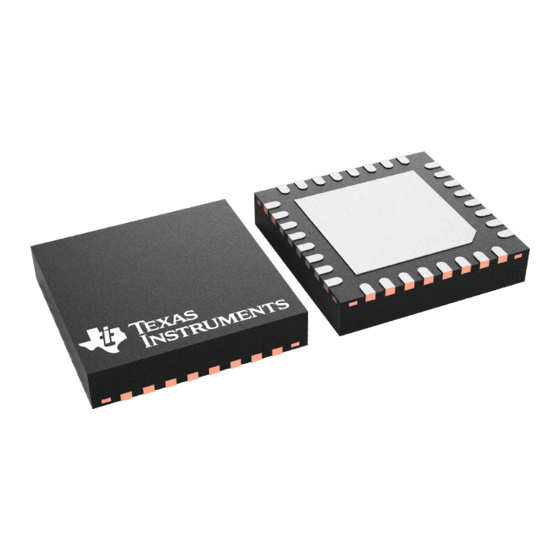
• 32-Pin QFN Package (5 mm × 5 mm) (RHB)
•
Public Transport or Event Ticketing
•
Medical Systems
•
Remote Sensor Applications
Support &
Reference
Community
Design
SLOS732G – JUNE 2011 – REVISED MARCH 2020
TRF7960A
Advertisement
Table of Contents

Related Manuals for Texas Instruments TRF7960A


Summary of Contents for Texas Instruments TRF7960A
-
Page 1: Device Overview
MCU can process the data in real time. The TRF7960A device supports a wide supply voltage range of 2.7 V to 5.5 V and data communication levels from 1.8 V to 5.5 V for the MCU I/O interface. -
Page 2: Application Block Diagram
(MSP430 or ARM) or SPI RX_IN 1 RX_IN 2 Supply Crystal Copyright © 2017, Texas Instruments Incorporated 2.7 V to 5.5 V 13.56 MHz Figure 1-1. Application Block Diagram Device Overview Copyright © 2011–2020, Texas Instruments Incorporated Submit Documentation Feedback... -
Page 3: Table Of Contents
........Related Products ......... 6.14 Register Description ....Terminal Configuration and Functions ..Applications, Implementation, and Layout ......... Pin Diagrams TRF7960A Reader System Using SPI With SS ........Signal Descriptions ..........Mode ..........Specifications ........System Design ......Absolute Maximum Ratings .... -
Page 4: Revision History
• Corrected typo (changed "...and 3.4 V for VDD_A and VDD_A" to "...and 3.4 V for VDD_A and VDD_X") in ....................Section 6.3, Supply Arrangements Revision History Copyright © 2011–2020, Texas Instruments Incorporated Submit Documentation Feedback Product Folder Links: TRF7960A... -
Page 5: Device Characteristics
TI Designs include schematic or block diagrams, BOMs, and design files to speed your time to market. Search and download designs at ti.com/tidesigns. Device Characteristics Copyright © 2011–2020, Texas Instruments Incorporated Submit Documentation Feedback Product Folder Links: TRF7960A... -
Page 6: Terminal Configuration And Functions
I/O pin for parallel communication I/O_2 I/O pin for parallel communication (1) SUP = Supply, INP = Input, BID = Bidirectional, OUT = Output Terminal Configuration and Functions Copyright © 2011–2020, Texas Instruments Incorporated Submit Documentation Feedback Product Folder Links: TRF7960A... - Page 7 Crystal or oscillator input Internally regulated supply (2.7 V to 3.4 V) for digital circuit and external devices (for example, an VDD_X MCU) Chip substrate ground Terminal Configuration and Functions Copyright © 2011–2020, Texas Instruments Incorporated Submit Documentation Feedback Product Folder Links: TRF7960A...
-
Page 8: Specifications
Recommended Operating Conditions over operating free-air temperature range (unless otherwise noted) UNIT Operating input voltage Operating ambient temperature –40 °C Operating virtual junction temperature –40 °C Specifications Copyright © 2011–2020, Texas Instruments Incorporated Submit Documentation Feedback Product Folder Links: TRF7960A... -
Page 9: Electrical Characteristics
10 MHz. This clock speed is acceptable only when external capacitive load is less than 30 pF. MISO driver has a typical output resistance of 400 Ω (12-ns time constant when 30-pF load is used). Specifications Copyright © 2011–2020, Texas Instruments Incorporated Submit Documentation Feedback Product Folder Links:... -
Page 10: Thermal Resistance Characteristics
10 MHz. This clock speed is acceptable only when external capacitive load is less than 30 pF. MISO driver has a typical output resistance of 400 Ω (12-ns time constant when 30-pF load is used). Specifications Copyright © 2011–2020, Texas Instruments Incorporated Submit Documentation Feedback Product Folder Links:... -
Page 11: Detailed Description
Figure 6-1. Functional Block Diagram Power Supplies The TRF7960A positive supply input VIN (pin 2) sources three internal regulators with output voltages VDD_RF, VDD_A, and VDD_X. All regulators require external bypass capacitors for supply noise filtering and must be connected as indicated in reference schematics. These regulators provide a high power supply reject ratio (PSRR) as required for RFID reader systems. -
Page 12: Supply Arrangements
External bypass capacitors for supply noise filtering must be used (per reference schematics). NOTE VIN must be the highest voltage supplied to the TRF7960A. RF Power Amplifier Regulator: VDD_RF The VDD_RF (pin 3) regulator is supplying the RF power amplifier. The voltage regulator can be set for either 5-V or 3-V operation. - Page 13 0x0B). Power Amplifier Supply: VDD_PA The power amplifier of the TRF7960A is supplied through VDD_PA (pin 4). The positive supply pin for the RF power amplifier is externally connected to the regulator output VDD_RF (pin 3). I/O Level Shifter Supply: VDD_I/O The TRF7960A has a separate supply input VDD_I/O (pin 16) for the build in I/O level shifter.
-
Page 14: Supply Regulator Settings
The Regulator Control register settings shown are for optimized power out. The automatic setting (normally 0x87) is optimized for best PSRR and noise reduction. Detailed Description Copyright © 2011–2020, Texas Instruments Incorporated Submit Documentation Feedback Product Folder Links: TRF7960A... - Page 15 4.8 ms 5 VDC Standby mode — 3.3 VDC Sleep mode 0.120 — 1.5 ms Power down <0.001 — Start (1) x = don't care Detailed Description Copyright © 2011–2020, Texas Instruments Incorporated Submit Documentation Feedback Product Folder Links: TRF7960A...
- Page 16 Mode 3 and Mode 4 (active modes with the entire RF section active, bit 5 = 1 of register 0x00) are the modes used for typical transmit and receive operations. Detailed Description Copyright © 2011–2020, Texas Instruments Incorporated Submit Documentation Feedback Product Folder Links:...
-
Page 17: Receiver - Analog Section
6.6.1 Main and Auxiliary Receiver The TRF7960A has two receiver inputs: RX_IN1 (pin 8) and RX_IN2 (pin 9). Each of the inputs is connected to an external capacitive voltage divider to ensure that the modulated signal from the tag is available on at least one of the two inputs. -
Page 18: Receiver - Digital Section
Receiver – Digital Section The output of the TRF7960A analog receiver block is a digitized subcarrier signal and is the input to the digital receiver block, which consists of two sections that partly overlap. The digitized subcarrier signal is a digital representation of the modulation signal on the RF envelope. - Page 19 6.7.1 Received Signal Strength Indicator (RSSI) The TRF7960A incorporates three independent RSSI building blocks: Internal Main RSSI, Internal Auxiliary RSSI, and External RSSI. The internal RSSI blocks are measuring the amplitude of the subcarrier signal, and the external RSSI block measures the amplitude of the RF carrier signal at the receiver input.
- Page 20 RX_IN1 input and the 3-bit code. RF Input Voltage Level at Pin RF_IN1 (mV ) Figure 6-3. Digital External RSSI Value vs RF Input Level Detailed Description Copyright © 2011–2020, Texas Instruments Incorporated Submit Documentation Feedback Product Folder Links: TRF7960A...
-
Page 21: Oscillator Section
The external shunt capacitors are calculated as two identical capacitors in series plus the stray capacitance of the TRF7960A and parasitic PCB capacitance in parallel to the crystal. The parasitic capacitance (C , stray and parasitic PCB capacitance) can be estimated at 4 to 5 pF (typical). -
Page 22: Transmitter - Analog Section
The digital part of the transmitter is a mirror of the receiver. The settings controlled the ISO Control register (0x01) are applied to the transmitter just like the receiver. In the TRF7960A default mode (ISO Mode), the TRF7960A automatically adds all the special signals like start of communication, end of communication, SOF, EOF, parity bits and CRC bytes. -
Page 23: Transmitter - External Power Amplifier Or Subcarrier Detector
6.11 Transmitter – External Power Amplifier or Subcarrier Detector The TRF7960A can be used in conjunction with an external TX power amplifier or external subcarrier detector for the receiver path. If this is the case, Bit B6 of the Regulator and I/O Control register (0x0B) must be set to 1. - Page 24 When the SPI interface is selected, the unused I/O_2, I/O_1, and I/O_0 pins must be hard-wired according Table 6-6. At power up, the TRF7960A IC samples the status of these three pins and then enters one of the possible SPI modes in Table 6-6.
- Page 25 The Command Mode is used to enter a command that results in reader action (for example, initialize transmission, enable reader, and turn reader on or off). The following examples show the expected communications between an MCU and the TRF7960A. Detailed Description Copyright ©...
- Page 26 Figure 6-5. Continuous Address Register Write Example Starting With Register 0x00 (Using SPI With SS Mode) Figure 6-6. Continuous Address Register Read Example Starting With Register 0x00 (Using SPI With SS Mode) Detailed Description Copyright © 2011–2020, Texas Instruments Incorporated Submit Documentation Feedback Product Folder Links: TRF7960A...
- Page 27 Figure 6-7. Single Address Register Write Example of Register 0x00 (Using SPI With SS Mode) Figure 6-8. Single Address Register Read Example of Register 0x00 (Using SPI With SS Mode) Detailed Description Copyright © 2011–2020, Texas Instruments Incorporated Submit Documentation Feedback Product Folder Links:...
- Page 28 Cmd x (Optional data or command) Stop Figure 6-9. Direct Command Example of Sending 0x0F (Reset) (Using SPI With SS Mode) The other Direct Command Codes from MCU to TRF7960A are described in Section 6.13. 6.12.2 FIFO Operation The FIFO is a 12-byte register at address 0x1F with byte storage locations 0 to 11. FIFO data is loaded in...
- Page 29 The number of bytes in a frame, transmitted or received, can be greater than 12 bytes. During transmission, the MCU loads the TRF7960A FIFO (or, during reception, the MCU removes data from the FIFO), and the FIFO counter counts the number of bytes being loaded into the FIFO. Meanwhile, the byte counter keeps track of the number of bytes being transmitted.
- Page 30 If the reader detects a receive error, the corresponding error flag is set (framing error, CRC error) in the IRQ Status register, indicating to the MCU that reception was not completed correctly. Detailed Description Copyright © 2011–2020, Texas Instruments Incorporated Submit Documentation Feedback Product Folder Links:...
- Page 31 When an SPI interface is used, I/O pins I/O_2, I/O_1, and I/O_0 must be hard-wired as specified in Table 6-6. On power up, the TRF7960A looks for the status of these pins; if they are not the same (not all high, or not all low), the reader enters into one of two possible SPI modes: •...
- Page 32 Data in can change only when SCLK is low, and it is read by the reader on the SCLK rising edge. Communication is terminated by the stop condition when the data in falling edge occurs during a high SCLK period. Detailed Description Copyright © 2011–2020, Texas Instruments Incorporated Submit Documentation Feedback Product Folder Links: TRF7960A...
- Page 33 B7 B6 B5 B4 B3 B2 B1 B0 Don't Care B7 B6 B5 B4 B3 B2 B1 B0 SLAVE SELECT Figure 6-18. Continuous Read Operation Using SPI With Slave Select Detailed Description Copyright © 2011–2020, Texas Instruments Incorporated Submit Documentation Feedback Product Folder Links: TRF7960A...
- Page 34 Figure 6-20. Inventory Command Sent From MCU to TRF7960A The TRF7960A reads these bytes from the MCU and then sends out Request Flags, Inventory Command, and Mask over the air to the ISO/IEC 15693 transponder. After these three bytes have been transmitted, an interrupt occurs from the reader to indicate back to the MCU that the transmission has been completed.
- Page 35 FIFO Status register, which indicates that there are at least 9 bytes to be read out. Detailed Description Copyright © 2011–2020, Texas Instruments Incorporated Submit Documentation Feedback Product Folder Links: TRF7960A...
- Page 36 6-24). IRQ register read shows RX is complete and FIFO register status shows one byte available, as expected and it is the E0, indicating ISO/IEC 15693 transponder. Detailed Description Copyright © 2011–2020, Texas Instruments Incorporated Submit Documentation Feedback Product Folder Links: TRF7960A...
- Page 37 In the example in Figure 6-25, the transponder is very close to the antenna, so a value of 0x7E is recovered. Figure 6-25. Reset FIFO and Read RSSI Detailed Description Copyright © 2011–2020, Texas Instruments Incorporated Submit Documentation Feedback Product Folder Links: TRF7960A...
- Page 38 Raw Digital ISO Coded Data Without Protocol Frame Packetization and Framing ISO Mode: Full ISO Framing and Error Checking (Typical Mode) Microcontroller Figure 6-26. User-Configurable Modes Detailed Description Copyright © 2011–2020, Texas Instruments Incorporated Submit Documentation Feedback Product Folder Links: TRF7960A...
- Page 39 0 becomes very useful. Step 1: Configure pins I/O_0 to I/O_2 for SPI with SS Step 2: Set pin 12 of the TRF7960A (ASK/OOK pin) to 0 for ASK or 1 for OOK Step 3: Program the TRF7960A registers The following registers must be explicitly set before going into direct mode.
- Page 40 Figure 6-29 shows an example of the receive data bits and framing level according to the ISO/IEC 14443 A standard (sourced from the ISO/IEC 14443 specification and TRF7960A air interface). Detailed Description Copyright © 2011–2020, Texas Instruments Incorporated...
- Page 41 Step 7: Exit direct mode 0 When an EOF is received, data transmission is over, and direct mode 0 can be terminated by sending a Stop condition (the SS signal goes high). The TRF7960A returns to ISO Mode (normal mode). Detailed Description Copyright ©...
-
Page 42: Direct Commands From Mcu To Reader
6.13.2 Reset FIFO (0x0F) The reset command clears the FIFO contents and FIFO Status register (0x1C). It also clears the register storing the collision error location (0x0E). Detailed Description Copyright © 2011–2020, Texas Instruments Incorporated Submit Documentation Feedback Product Folder Links: TRF7960A... - Page 43 5 to 6. The nominal relationship between the RF peak level and RSSI code is described in Table 6-13 and in Section 6.7.1.1. Detailed Description Copyright © 2011–2020, Texas Instruments Incorporated Submit Documentation Feedback Product Folder Links: TRF7960A...
- Page 44 The Clo0 and Clo1 bits in the Modulator and SYS_CLK Control register (0x09), which define the microcontroller frequency available on the SYS_CLK pin, are the only 2 bits in the configuration registers that are not cleared during protocol selection. Detailed Description Copyright © 2011–2020, Texas Instruments Incorporated Submit Documentation Feedback Product Folder Links: TRF7960A...
-
Page 45: Register Description
TRF7960A www.ti.com SLOS732G – JUNE 2011 – REVISED MARCH 2020 6.14 Register Description 6.14.1 Register Overview Table 6-15 lists the registers available in the TRF7960A. These registers are described in the following sections. Table 6-15. Register Overview ADDRESS REGISTER READ/WRITE... - Page 46 Allows enable of the receiver by bit 5 of this register 1 = 5-V operation vrs5_3 Selects the VIN voltage range 0 = 3-V operation Detailed Description Copyright © 2011–2020, Texas Instruments Incorporated Submit Documentation Feedback Product Folder Links: TRF7960A...
- Page 47 FeliCa 424 kbps (1) For ISO/IEC 14443 A or B, when bit rate of TX is different from RX, settings can be made in register 0x02 or 0x03. Detailed Description Copyright © 2011–2020, Texas Instruments Incorporated Submit Documentation Feedback Product Folder Links:...
- Page 48 TX For ISO/IEC 14443 A high-bit-rate coding and decoding 1 = Parity odd except last byte, parity-2rx which is even for RX Unused Unused Unused Detailed Description Copyright © 2011–2020, Texas Instruments Incorporated Submit Documentation Feedback Product Folder Links: TRF7960A...
- Page 49 Timer length All bits low = timer disabled (0x00) tm_length2 Timer length tm_length1 Timer length Preset to 0x00 for all other protocols. tm_length0 Timer length LSB Detailed Description Copyright © 2011–2020, Texas Instruments Incorporated Submit Documentation Feedback Product Folder Links: TRF7960A...
- Page 50 NoResp2 755 µs for ISO/IEC 15693 high data rate (TI Tag-It HF-I) NoResp1 1812 µs for ISO/IEC 15693 low data rate (TI Tag-It HF-I) NoResp0 Detailed Description Copyright © 2011–2020, Texas Instruments Incorporated Submit Documentation Feedback Product Folder Links: TRF7960A...
- Page 51 The following default timings are preset by the ISO Control register (0x01): 9.44 µs for FeliCa Rxw2 66 µs for ISO/IEC 14443 A and B Rxw1 293 µs for ISO/IEC 15693 (TI Tag-It HF-I) Rxw0 Detailed Description Copyright © 2011–2020, Texas Instruments Incorporated Submit Documentation Feedback Product Folder Links: TRF7960A...
- Page 52 The frequency of SYS_CLK (pin 27) is programmable by bits B4 and B5 of this register. The frequency of the TRF7960A system clock oscillator is divided by 1, 2, or 4 resulting in available SYS_CLK frequencies of 13.56 MHz, 6.78 MHz, or 3.39 MHz, respectively.
- Page 53 The setting of bits B4, B5, B6, and B7 to zero selects band-pass characteristic of 240 kHz to 1.4 MHz. This is appropriate for ISO/IEC 14443 B, FeliCa protocol, and ISO/IEC 14443 A higher bit rates (212 kbps and 424 kbps). Detailed Description Copyright © 2011–2020, Texas Instruments Incorporated Submit Documentation Feedback Product Folder Links: TRF7960A...
- Page 54 VDD_RF = 4.5 V, VDD_A = 3.5 V, VDD_X = 3.4 V VDD_RF = 4.4 V, VDD_A = 3.5 V, VDD_X = 3.4 V VDD_RF = 4.3 V, VDD_A = 3.5 V, VDD_X = 3.4 V Detailed Description Copyright © 2011–2020, Texas Instruments Incorporated Submit Documentation Feedback Product Folder Links: TRF7960A...
- Page 55 3-V system Automatic regulator setting with 250-mV difference Automatic regulator setting with 350-mV difference Automatic regulator setting with 400-mV difference (1) x = don't care Detailed Description Copyright © 2011–2020, Texas Instruments Incorporated Submit Documentation Feedback Product Folder Links: TRF7960A...
- Page 56 IRQ Status register. This register provides information available about TRF7960A IRQ, TX, and RX status. Default Value: 0x00, set at POR = H or EN = L and at each write to the ISO Control register (0x01). The register is also automatically reset at the end of a read phase.
- Page 57 Bit position of collision. B7 is the register shows the bit position of error. Either frame, SOF/EOF, MSB. Col3 parity, or CRC error. Col2 Col1 Col0 Detailed Description Copyright © 2011–2020, Texas Instruments Incorporated Submit Documentation Feedback Product Folder Links: TRF7960A...
- Page 58 Active channel is the default and can be set with option bit B3 = 0 of rssi_1 Main channel RSSI the Chip Status Control register (0x00). LSB RSSI value of Main RX rssi_0 (RX_IN1) Detailed Description Copyright © 2011–2020, Texas Instruments Incorporated Submit Documentation Feedback Product Folder Links: TRF7960A...
- Page 59 DESCRIPTION test_rf_level RF level test test_io1 I/O test Not implemented test_io0 test_dec Decoder test mode clock_su Coder clock 13.56 MHz For faster test of coders Detailed Description Copyright © 2011–2020, Texas Instruments Incorporated Submit Documentation Feedback Product Folder Links: TRF7960A...
- Page 60 Number of complete byte bn[6] Middle nibble of complete intended bytes to be transmitted Txl5 Number of complete byte bn[5] Txl4 Number of complete byte bn[4] Detailed Description Copyright © 2011–2020, Texas Instruments Incorporated Submit Documentation Feedback Product Folder Links: TRF7960A...
- Page 61 This value is taken into account only when broken byte flag is set. Broken byte number of bits bb[0] Broken byte flag B0 = 1 indicates that last byte is not complete 8 bits wide. Detailed Description Copyright © 2011–2020, Texas Instruments Incorporated Submit Documentation Feedback Product Folder Links: TRF7960A...
-
Page 62: Applications, Implementation, And Layout
7.1.1 General Application Considerations Figure 7-1 shows the TRF7960A application schematic optimized for both ISO/IEC 15693 and ISO/IEC 14443 systems using the serial port interface (SPI). Short SPI lines, proper isolation to radio frequency lines, and a proper ground area are essential to avoid interference. The recommended clock frequency on the DATA_CLK line is 2 MHz. -
Page 63: System Design
7.2.2 Impedance Matching TX_Out (Pin 5) to 50 Ω The output impedance of the TRF7960A when operated at full power out setting is nominally 4 + j0 Ω (4 Ω real). This impedance must be matched to a resonant circuit, and TI recommends a matching circuit from 4 Ω... - Page 64 7.2.3 Reader Antenna Design Guidelines For HF antenna design considerations using the TRF7960A, see the following documentation: Antenna Matching for the TRF7960 RFID Reader TRF7960TB HF RFID Reader Module User's...
-
Page 65: Device And Documentation Support
Revision A = Silicon revision Packaging Information Package or www.ti.com/package Distribution R = Large reel T = Small reel Figure 8-1. Device Nomenclature Device and Documentation Support Copyright © 2011–2020, Texas Instruments Incorporated Submit Documentation Feedback Product Folder Links: TRF7960A... -
Page 66: Tools And Software
TRF7960A C Code Samples Sample source code for direct register control of the device functions. Documentation Support The following documents describe the TRF7960A device. Copies of these documents are available on the Internet at www.ti.com. Receiving Notification of Document Updates To receive notification of documentation updates—including silicon errata—go to the product folder for... -
Page 67: Electrostatic Discharge Caution
SLOS732G – JUNE 2011 – REVISED MARCH 2020 Electrostatic Discharge Caution This integrated circuit can be damaged by ESD. Texas Instruments recommends that all integrated circuits be handled with appropriate precautions. Failure to observe proper handling and installation procedures can cause damage. -
Page 68: Mechanical, Packaging, And Orderable Information
This data is subject to change without notice and revision of this document. For browser-based versions of this data sheet, refer to the left-hand navigation. Mechanical, Packaging, and Orderable Information Copyright © 2011–2020, Texas Instruments Incorporated Submit Documentation Feedback Product Folder Links:... - Page 69 PACKAGE OPTION ADDENDUM www.ti.com 10-Dec-2020 PACKAGING INFORMATION Orderable Device Status Package Type Package Pins Package Eco Plan Lead finish/ MSL Peak Temp Op Temp (°C) Device Marking Samples Drawing Ball material (4/5) TRF7960ARHBR ACTIVE VQFN 3000 RoHS & Green NIPDAU Level-2-260C-1 YEAR -40 to 110 7960A...
- Page 70 PACKAGE OPTION ADDENDUM www.ti.com 10-Dec-2020 Addendum-Page 2...
- Page 71 PACKAGE MATERIALS INFORMATION www.ti.com 19-Oct-2020 TAPE AND REEL INFORMATION *All dimensions are nominal Device Package Package Pins Reel Reel Pin1 Type Drawing Diameter Width (mm) (mm) (mm) (mm) (mm) Quadrant (mm) W1 (mm) TRF7960ARHBR VQFN 3000 330.0 12.4 12.0 TRF7960ARHBT VQFN 180.0 12.4...
- Page 72 PACKAGE MATERIALS INFORMATION www.ti.com 19-Oct-2020 *All dimensions are nominal Device Package Type Package Drawing Pins Length (mm) Width (mm) Height (mm) TRF7960ARHBR VQFN 3000 853.0 449.0 35.0 TRF7960ARHBT VQFN 210.0 185.0 35.0 Pack Materials-Page 2...
- Page 73 GENERIC PACKAGE VIEW RHB 32 VQFN - 1 mm max height PLASTIC QUAD FLATPACK - NO LEAD 5 x 5, 0.5 mm pitch Images above are just a representation of the package family, actual package may vary. Refer to the product data sheet for package details. 4224745/A www.ti.com...
- Page 74 PACKAGE OUTLINE RHB0032E VQFN - 1 mm max height SCALE 3.000 PLASTIC QUAD FLATPACK - NO LEAD PIN 1 INDEX AREA (0.1) SIDE WALL DETAIL OPTIONAL METAL THICKNESS 20.000 1 MAX SEATING PLANE 0.05 0.08 C 0.00 2X 3.5 (0.2) TYP 3.45 0.1 EXPOSED THERMAL PAD...
- Page 75 4223442/B 08/2019 NOTES: (continued) 4. This package is designed to be soldered to a thermal pad on the board. For more information, see Texas Instruments literature number SLUA271 (www.ti.com/lit/slua271). 5. Vias are optional depending on application, refer to device data sheet. If any vias are implemented, refer to their locations shown on this view.
- Page 76 EXAMPLE STENCIL DESIGN RHB0032E VQFN - 1 mm max height PLASTIC QUAD FLATPACK - NO LEAD 4X ( 1.49) (0.845) (R0.05) TYP 32X (0.6) 32X (0.25) 28X (0.5) (0.845) SYMM (4.8) METAL SYMM (4.8) SOLDER PASTE EXAMPLE BASED ON 0.125 mm THICK STENCIL EXPOSED PAD 33: 75% PRINTED SOLDER COVERAGE BY AREA UNDER PACKAGE SCALE:20X...
- Page 77 TI products. TI’s provision of these resources does not expand or otherwise alter TI’s applicable warranties or warranty disclaimers for TI products. Mailing Address: Texas Instruments, Post Office Box 655303, Dallas, Texas 75265 Copyright © 2020, Texas Instruments Incorporated...