Table of Contents
Advertisement
Quick Links
www.ti.com
User's Guide
TPSM8D6C24EVM-2V0 User's Guide
This user's guide describes the characteristics, operation, and use of the TPSM8D6C24EVM-2V0 evaluation
module (EVM). In addition, the user's guide includes test information, descriptions, and results. A complete
schematic diagram, printed circuit board layouts, and bill of materials are also included in this document.
1 Description..............................................................................................................................................................................
1.1 Before You Begin...............................................................................................................................................................
1.2 Features.............................................................................................................................................................................
2 Electrical Performance Specifications.................................................................................................................................
3
Schematic................................................................................................................................................................................5
Setup................................................................................................................................................................................6
4.1 Test and Configuration Software........................................................................................................................................
4.2 Test Equipment..................................................................................................................................................................
4.4 Evaluating Split Rail Input..................................................................................................................................................
5.1 Configuration Procedure....................................................................................................................................................
6 Test Procedure........................................................................................................................................................................
6.1 Line and Load Regulation and Efficiency Measurement Procedure..................................................................................
6.2 Efficiency Measurement Test Points..................................................................................................................................
6.3 Control Loop Gain and Phase Measurement Procedure.................................................................................................
7.1 Efficiency..........................................................................................................................................................................
7.2 Load Regulation...............................................................................................................................................................
Regulation.................................................................................................................................................................11
7.4 Transient Response.........................................................................................................................................................
7.5 Control Loop Bode Plot....................................................................................................................................................
7.6 Output Ripple...................................................................................................................................................................
On........................................................................................................................................................................14
Off........................................................................................................................................................................14
7.9 Thermal Image.................................................................................................................................................................
8 EVM Assembly Drawing and PCB Layout..........................................................................................................................
9 Bill of Materials.....................................................................................................................................................................
10 Using the Fusion GUI.........................................................................................................................................................
10.1 Opening the Fusion GUI................................................................................................................................................
10.2 General Settings............................................................................................................................................................
10.3 Changing ON_OFF_CONFIG........................................................................................................................................
10.4 Pop-Up for Some Commands While Conversion is Enabled.........................................................................................
10.5 SMBALERT# Mask........................................................................................................................................................
10.6 Device Info.....................................................................................................................................................................
Commands..........................................................................................................................................................29
Config........................................................................................................................................................................30
Strapping..................................................................................................................................................................31
10.10 Monitor.........................................................................................................................................................................
10.11 Status...........................................................................................................................................................................
Figure 3-1. TPSM8D6C24EVM-2V0 Schematic..........................................................................................................................
Figure 7-1. VOUT_A Efficiency..................................................................................................................................................
SLUUCK6 - DECEMBER 2021
Submit Document Feedback
ABSTRACT
Table of Contents
Connectors....................................................................................................................7
GUI............................................................................................................................9
Curves.......................................................................................................11
List of Figures
Copyright © 2021 Texas Instruments Incorporated
Table of Contents
TPSM8D6C24EVM-2V0 User's Guide
3
3
3
4
6
6
8
9
9
9
9
10
11
11
12
12
13
15
16
19
23
23
24
24
26
27
28
32
33
5
11
1
Advertisement
Table of Contents

Related Manuals for Texas Instruments TPSM8D6C24EVM-2V0


Summary of Contents for Texas Instruments TPSM8D6C24EVM-2V0
-
Page 1: Table Of Contents
TPSM8D6C24EVM-2V0 User's Guide ABSTRACT This user's guide describes the characteristics, operation, and use of the TPSM8D6C24EVM-2V0 evaluation module (EVM). In addition, the user's guide includes test information, descriptions, and results. A complete schematic diagram, printed circuit board layouts, and bill of materials are also included in this document. - Page 2 Figure 7-19. Thermal Image..............................Figure 8-1. TPSM8D6C24EVM-2V0 Top Side Component View (Top View)................16 Figure 8-2. TPSM8D6C24EVM-2V0 Bottom Side Component View (Bottom View)..............Figure 8-3. TPSM8D6C24EVM-2V0 Top Copper (Top View)....................Figure 8-4. TPSM8D6C24EVM-2V0 Internal Layer 1 (Top View)....................Figure 8-5. TPSM8D6C24EVM-2V0 Internal Layer 2 (Top View)....................
-
Page 3: Description
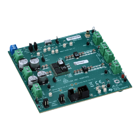
Description 1 Description The TPSM8D6C24 is a configurable dual-output buck converter module. The TPSM8D6C24EVM-2V0 uses a nominal 12-V bus to produce a regulated 0.8-V and 1.2-V output at up to 35 A of load current each. The TPSM8D6C24EVM-2V0 demonstrates the dual output capability. -
Page 4: Electrical Performance Specifications
Table 2-1 lists the electrical performance specifications in room temperature (20 to 25°C). Characteristics are given for an input voltage of V = 12 V, unless otherwise specified. Table 2-1. TPSM8D6C24EVM-2V0 Electrical Performance Specifications Parameter Test Conditions Unit Input Characteristics... -
Page 5: Schematic
DATA TP 25 TP 26 S MBALRT P MBus DATA P GND P GND P GND TP 27 P GND Figure 3-1. TPSM8D6C24EVM-2V0 Schematic SLUUCK6 – DECEMBER 2021 TPSM8D6C24EVM-2V0 User's Guide Submit Document Feedback Copyright © 2021 Texas Instruments Incorporated... -
Page 6: Test Setup
The TI Fusion Digital Power Designer is the graphical user interface (GUI) used to configure and monitor the Texas Instruments TPSM8D6C24 power converter installed on this evaluation module. The application uses the PMBus protocol to communicate with the controller over serial bus by way of a TI USB adapter described in Section 4.2.6. -
Page 7: List Of Test Points, Jumpers, And Connectors
PMBus to AVIN Short to connect USB-to-GPIO 3.3V to AVIN Table 4-3 lists the options for the EN/UVLO pin selections on JP2 and JP4. SLUUCK6 – DECEMBER 2021 TPSM8D6C24EVM-2V0 User's Guide Submit Document Feedback Copyright © 2021 Texas Instruments Incorporated... -
Page 8: Evaluating Split Rail Input
EN/UVLO will need to be changed. Alternately, move the CNTL jumpers to CNTL_INPUT position and use the control signal to enable conversion or use the ON_OFF_CONFIG and OPERATION commands to enable conversion. TPSM8D6C24EVM-2V0 User's Guide SLUUCK6 – DECEMBER 2021 Submit Document Feedback Copyright © 2021 Texas Instruments Incorporated... -
Page 9: Evm Configuration Using The Fusion Gui
The pair of test points are connected to the PVIN/PGND pins of U1. The voltage drop between input terminal to the device pins is included for efficiency measurement. Input voltage measurement point PGND for VIN– (GND) SLUUCK6 – DECEMBER 2021 TPSM8D6C24EVM-2V0 User's Guide Submit Document Feedback Copyright © 2021 Texas Instruments Incorporated... -
Page 10: Control Loop Gain And Phase Measurement Procedure
VOUT– (GND) 6.3 Control Loop Gain and Phase Measurement Procedure The TPSM8D6C24EVM-2V0 includes a 49.9-Ω series resistor in the feedback loop for V . The resistor is accessible at the test points TP7, TP8, TP19, and TP20 for loop response analysis. These test points should be used during loop response measurements as the perturbation injecting points for the loop. -
Page 11: Performance Data And Typical Characteristic Curves
7 Performance Data and Typical Characteristic Curves Figure 7-1 through Figure 7-19 present typical performance curves for the TPSM8D6C24EVM-2V0. The input voltage is 12 V and the oscilloscope measurements use 20-MHz bandwidth limiting, unless otherwise noted. 7.1 Efficiency PVIN = 5 V... -
Page 12: Transient Response
Figure 7-8. VOUT_B Transient Response 7.5 Control Loop Bode Plot Figure 7-9. VOUT_A Bode Plot, 35-A Load Figure 7-10. VOUT_B Bode Plot, 35-A Load TPSM8D6C24EVM-2V0 User's Guide SLUUCK6 – DECEMBER 2021 Submit Document Feedback Copyright © 2021 Texas Instruments Incorporated... -
Page 13: Output Ripple
Figure 7-11. VOUT_A Output Ripple, No Load Figure 7-12. VOUT_B Output Ripple, No Load Figure 7-13. VOUT_A Output Ripple, 35-A Load Figure 7-14. VOUT_B Output Ripple, 35-A Load SLUUCK6 – DECEMBER 2021 TPSM8D6C24EVM-2V0 User's Guide Submit Document Feedback Copyright © 2021 Texas Instruments Incorporated... -
Page 14: Control On
35-A outputs. Figure 7-17. VOUT_A Shutdown From Control, 35- Figure 7-18. VOUT_B Shutdown From Control, 35- A CC Load A CC Load TPSM8D6C24EVM-2V0 User's Guide SLUUCK6 – DECEMBER 2021 Submit Document Feedback Copyright © 2021 Texas Instruments Incorporated... -
Page 15: Thermal Image
Performance Data and Typical Characteristic Curves 7.9 Thermal Image Figure 7-19 shows the TPSM8D6C24EVM-2V0 thermal image. = 12 V, I = 35 A, I = 35A, Airflow = 200 LFM, 10 minute soak OUTA OUTB Figure 7-19. Thermal Image SLUUCK6 –... -
Page 16: Evm Assembly Drawing And Pcb Layout
8 EVM Assembly Drawing and PCB Layout Figure 8-1 through Figure 8-8 show the design of the TPSM8D6C24EVM-2V0 printed circuit board. Figure 8-1. TPSM8D6C24EVM-2V0 Top Side Figure 8-2. TPSM8D6C24EVM-2V0 Bottom Side Component View (Top View) Component View (Bottom View) Figure 8-3. -
Page 17: Figure 8-5. Tpsm8D6C24Evm-2V0 Internal Layer 2 (Top View)
EVM Assembly Drawing and PCB Layout Figure 8-5. TPSM8D6C24EVM-2V0 Internal Layer 2 Figure 8-6. TPSM8D6C24EVM-2V0 Internal Layer 3 (Top View) (Top View) Figure 8-7. TPSM8D6C24EVM-2V0 Internal Layer 4 Figure 8-8. TPSM8D6C24EVM-2V0 Internal Layer 5 (Top View) (Top View) SLUUCK6 – DECEMBER 2021... -
Page 18: Figure 8-9. Tpsm8D6C24Evm-2V0 Internal Layer 6 (Top View)
EVM Assembly Drawing and PCB Layout www.ti.com Figure 8-9. TPSM8D6C24EVM-2V0 Internal Layer 6 Figure 8-10. TPSM8D6C24EVM-2V0 Internal Bottom (Top View) Layer (Top View) TPSM8D6C24EVM-2V0 User's Guide SLUUCK6 – DECEMBER 2021 Submit Document Feedback Copyright © 2021 Texas Instruments Incorporated... -
Page 19: Bill Of Materials
Bill of Materials 9 Bill of Materials Table 9-1 lists the BOM for the TPSM8D6C24EVM-2V0. Table 9-1. TPSM8D624EVM-2V0 Bill of Materials Designator Quantity Value Description PackageReference PartNumber Manufacturer Alternate Alternate PartNumber Manufacturer !PCB1 Printed Circuit Board BSR192 C1, C7, C8, 100 μF... - Page 20 26.1 k RES, 26.1 k, 1%, 0.1 W, CRCW060326K1FKEA Vishay-Dale 0603 68.1 k RES, 68.1 k, 0.1%, 0.1 W, RG1608P-6812-B-T5 Susumu Co Ltd 0603 TPSM8D6C24EVM-2V0 User's Guide SLUUCK6 – DECEMBER 2021 Submit Document Feedback Copyright © 2021 Texas Instruments Incorporated...
- Page 21 Fiducial mark. There is FID3, FID4, nothing to buy or mount. FID5, FID6 R5, R11 10.0 k RES, 10.0 k, 1%, 0.1 W, ERJ-2RKF1002X Panasonic 0402 SLUUCK6 – DECEMBER 2021 TPSM8D6C24EVM-2V0 User's Guide Submit Document Feedback Copyright © 2021 Texas Instruments Incorporated...
- Page 22 RES, 53.6 k, 1%, 0.1 W, CRCW060353K6FKEA Vishay-Dale AEC-Q200 Grade 0, 0603 RES, 0, 5%, 0.1 W, AEC- ERJ-3GEY0R00V Panasonic Q200 Grade 0, 0603 TPSM8D6C24EVM-2V0 User's Guide SLUUCK6 – DECEMBER 2021 Submit Document Feedback Copyright © 2021 Texas Instruments Incorporated...
-
Page 23: Using The Fusion Gui
The Fusion GUI should include IC_DEVICE_ID in the scanning mode to find TPSM8D6C24. The EVM needs power to be recognized by the Fusion GUI. See Section 5 for the recommended procedure. Figure 10-1. Select Device Scanning Mode SLUUCK6 – DECEMBER 2021 TPSM8D6C24EVM-2V0 User's Guide Submit Document Feedback Copyright © 2021 Texas Instruments Incorporated... -
Page 24: General Settings
By default the TPSM8D6C24 is configured to CONTROL Pin Only. This is the EN/UVLO pin. TPSM8D6C24EVM-2V0 User's Guide SLUUCK6 – DECEMBER 2021 Submit Document Feedback Copyright © 2021 Texas Instruments Incorporated... -
Page 25: Figure 10-3. Configure - On_Off_Config
Using the Fusion GUI Figure 10-3. Configure – ON_OFF_CONFIG SLUUCK6 – DECEMBER 2021 TPSM8D6C24EVM-2V0 User's Guide Submit Document Feedback Copyright © 2021 Texas Instruments Incorporated... -
Page 26: Pop-Up For Some Commands While Conversion Is Enabled
Stop Power Conversion then Close and continue. The GUI will automatically disable conversion, write the new value, and enable conversion again. Figure 10-4. Pop-up When Trying to Change FREQUENCY_SWITCH With Conversion Enabled TPSM8D6C24EVM-2V0 User's Guide SLUUCK6 – DECEMBER 2021 Submit Document Feedback Copyright © 2021 Texas Instruments Incorporated... -
Page 27: Smbalert# Mask
The sources of SMBALERT which can be masked are found and configured on the SMBALERT # Mask tab (Figure 10-5). Figure 10-5. Configure – SMBALERT # Mask SLUUCK6 – DECEMBER 2021 TPSM8D6C24EVM-2V0 User's Guide Submit Document Feedback Copyright © 2021 Texas Instruments Incorporated... -
Page 28: Device Info
The device information, Write Protection options, the configuration of Vout Scale Loop, Vout Transition Rate, and Iout Cal Offset are found on the Device Info tab (see Figure 10-6). Figure 10-6. Configure – Device Info TPSM8D6C24EVM-2V0 User's Guide SLUUCK6 – DECEMBER 2021 Submit Document Feedback Copyright © 2021 Texas Instruments Incorporated... -
Page 29: Phase Commands
Using the Fusion GUI 10.7 Phase Commands Use the Phase Command tab (see Figure 10-7) to calibrate the IOUT/Temp of each phase. Figure 10-7. Phase Commands SLUUCK6 – DECEMBER 2021 TPSM8D6C24EVM-2V0 User's Guide Submit Document Feedback Copyright © 2021 Texas Instruments Incorporated... -
Page 30: All Config
Use the All Config tab (Figure 10-8) to configure all of the configurable parameters, which also shows other details like Hex encoding. Figure 10-8. Configure – All Config TPSM8D6C24EVM-2V0 User's Guide SLUUCK6 – DECEMBER 2021 Submit Document Feedback Copyright © 2021 Texas Instruments Incorporated... -
Page 31: Pin Strapping
PMBus commands at power up. The EEPROM Value column shows the values currently configured to the related PMBus commands. Figure 10-9. Configure – Pin Strapping SLUUCK6 – DECEMBER 2021 TPSM8D6C24EVM-2V0 User's Guide Submit Document Feedback Copyright © 2021 Texas Instruments Incorporated... -
Page 32: Monitor
With two devices stacked together, the Iout reading is the total load supported by both devices. There is also an Iout which shows the current in each phase. Figure 10-10. Monitor Screen TPSM8D6C24EVM-2V0 User's Guide SLUUCK6 – DECEMBER 2021 Submit Document Feedback Copyright © 2021 Texas Instruments Incorporated... -
Page 33: Status
Using the Fusion GUI 10.11 Status Selecting Status screen from lower left corner (Figure 10-11) shows the status of the device. Figure 10-11. Status Screen SLUUCK6 – DECEMBER 2021 TPSM8D6C24EVM-2V0 User's Guide Submit Document Feedback Copyright © 2021 Texas Instruments Incorporated... - Page 34 STANDARD TERMS FOR EVALUATION MODULES Delivery: TI delivers TI evaluation boards, kits, or modules, including any accompanying demonstration software, components, and/or documentation which may be provided together or separately (collectively, an “EVM” or “EVMs”) to the User (“User”) in accordance with the terms set forth herein.
- Page 35 www.ti.com Regulatory Notices: 3.1 United States 3.1.1 Notice applicable to EVMs not FCC-Approved: FCC NOTICE: This kit is designed to allow product developers to evaluate electronic components, circuitry, or software associated with the kit to determine whether to incorporate such items in a finished product and software developers to write software applications for use with the end product.
- Page 36 www.ti.com Concernant les EVMs avec antennes détachables Conformément à la réglementation d'Industrie Canada, le présent émetteur radio peut fonctionner avec une antenne d'un type et d'un gain maximal (ou inférieur) approuvé pour l'émetteur par Industrie Canada. Dans le but de réduire les risques de brouillage radioélectrique à...
- Page 37 www.ti.com EVM Use Restrictions and Warnings: 4.1 EVMS ARE NOT FOR USE IN FUNCTIONAL SAFETY AND/OR SAFETY CRITICAL EVALUATIONS, INCLUDING BUT NOT LIMITED TO EVALUATIONS OF LIFE SUPPORT APPLICATIONS. 4.2 User must read and apply the user guide and other available documentation provided by TI regarding the EVM prior to handling or using the EVM, including without limitation any warning or restriction notices.
- Page 38 Notwithstanding the foregoing, any judgment may be enforced in any United States or foreign court, and TI may seek injunctive relief in any United States or foreign court. Mailing Address: Texas Instruments, Post Office Box 655303, Dallas, Texas 75265 Copyright © 2019, Texas Instruments Incorporated...
- Page 39 TI products. TI’s provision of these resources does not expand or otherwise alter TI’s applicable warranties or warranty disclaimers for TI products. TI objects to and rejects any additional or different terms you may have proposed. IMPORTANT NOTICE Mailing Address: Texas Instruments, Post Office Box 655303, Dallas, Texas 75265 Copyright © 2021, Texas Instruments Incorporated...