Table of Contents
Advertisement
TABLE OF CONTENTS
1 Safety Precautions----------------------------------------------- 3
1.1. General Guidelines---------------------------------------- 3
1.2. Caution for AC Cord (For EB only)-------------------- 4
1.3. Before Repair and Adjustment ------------------------- 5
1.4. Protection Circuitry ---------------------------------------- 5
1.5. Caution For Fuse Replacement------------------------ 5
1.6. Safety Part Information----------------------------------- 6
2 Warning -------------------------------------------------------------- 8
Home Theater Audio System
Model No.
Product Color: (K)...Black Type
PAGE
2.1. Prevention of Electrostatic Discharge (ESD)
to Electrostatically Sensitive (ES) Devices ----------8
2.2. Service caution based on Legal restrictions
(Lead Free Solder, (PbF))--------------------------------9
3 Service Navigation --------------------------------------------- 10
3.1. Service Information -------------------------------------- 10
4 Specifications ---------------------------------------------------- 11
5 Location of Controls and Components------------------ 12
© Panasonic Corporation 2015. All rights reserved.
Unauthorized copying and distribution is a violation of
law.
SU-HTB485EB
SU-HTB485EG
SU-HTB485GN
SB-HWA480EB
SB-HWA480GN
SC-HTB485EB
SC-HTB485EG
SC-HTB485GN
PSG1503003CE
PAGE
Advertisement
Table of Contents
Troubleshooting

Related Manuals for Panasonic SU-HTB485EB


Summary of Contents for Panasonic SU-HTB485EB
-
Page 1: Table Of Contents
3.1. Service Information -------------------------------------- 10 1.6. Safety Part Information----------------------------------- 6 4 Specifications ---------------------------------------------------- 11 2 Warning -------------------------------------------------------------- 8 5 Location of Controls and Components------------------ 12 © Panasonic Corporation 2015. All rights reserved. Unauthorized copying and distribution is a violation of law. - Page 2 5.1. Main Unit & Active Subwoofer Key Button Operations ------------------------------------------------- 12 5.2. Remote Control Key Button Operations------------ 13 6 Service Mode ----------------------------------------------------- 14 6.1. Service Mode Table 1 ----------------------------------- 14 6.2. Service Mode Table 2 ----------------------------------- 15 6.3. Service Mode Software Version Check Table----- 16 6.4.
-
Page 3: Safety Precautions
1 Safety Precautions 1.1. General Guidelines 1. IMPORTANT SAFETY NOTICE There are special components used in this equipment which are important for safety. These parts are marked by in the Schematic Diagrams, Circuit Board Layout, Exploded Views and Replacement Parts List. It is essential that these critical parts should be replaced with manufacturer’s specified parts to prevent X-RADIATION, shock, fire, or other hazards. -
Page 4: Caution For Ac Cord (For Eb Only)
1.2. Caution for AC Cord (For EB only) Figure 1-2... -
Page 5: Before Repair And Adjustment
1.3. Before Repair and Adjustment 1.3.1. Main Speaker Unit (SU-HTB485) Disconnect AC power, discharge AC Capacitors (C5700, C5701, C5702, C5703, C5704 and C5705) through a 10W, 1W resistor to ground. Caution : DO NOT SHORT-CIRCUIT DIRECTLY (with a screwdriver blade, for instance), as this may destroy solid state devices. After repairs are completed, restore power gradually using a variac, to avoid overcurrent. -
Page 6: Safety Part Information
1.6. Safety Part Information Safety Parts List: There are special components used in this equipment which are important for safety. These parts are marked by in the Schematic Diagrams & Replacement Parts List. It is essential that these critical parts should be replaced with manufacturer’s specified parts to prevent shock, fire or other hazards. - Page 7 1.6.3. System (SC-HTB485) Safety Ref. No. Part No. Part Name & Description Remarks K2CJ2YY00101 AC CORD K2CQ2YY00119 AC CORD K2CT2YY00097 AC CORD RQT0A04-B O/I BOOK (En) RQT0A05-D O/I BOOK (Ge/Fr/It) RQT0A06-E O/I BOOK (Sw/Da/Du) RQT0A14-R O/I BOOK (Ru/Ur)
-
Page 8: To Electrostatically Sensitive (Es) Devices
2 Warning 2.1. Prevention of Electrostatic Discharge (ESD) to Electrostatically Sensi- tive (ES) Devices Some semiconductor (solid state) devices can be damaged easily by static electricity. Such components commonly are called Elec- trostatically Sensitive (ES) Devices. The following techniques should be used to help reduce the incidence of component damage caused by electrostatic discharge (ESD). -
Page 9: (Lead Free Solder, (Pbf))
2.2. Service caution based on Legal restrictions (Lead Free Solder, (PbF)) The lead free solder has been used in the mounting process of all electrical components on the printed circuit boards used for this equipment in considering the globally environmental conservation. The normal solder is the alloy of tin (Sn) and lead (Pb). -
Page 10: Service Navigation
3 Service Navigation 3.1. Service Information This service manual contains technical information which will allow service personnel’s to understand and service this model. Please place orders using the parts list and not the drawing reference numbers. If the circuit is changed or modified, this information will be followed by supplement service manual to be filed with original service manual. -
Page 11: Specifications
4 Specifications Bluetooth® system specifica- ® Bluetooth Ver. 2.1+EDR tion Wireless equipment classifica- Class 2 tion Amplifier Section Supported profiles A2DP RMS output power: Dolby Digital Mode Operating frequency 2.4 GHz band FH-SS 60 W per channel (6 Ω), 1 kHz, Front ch (L, R ch) Operating distance 10 m (33 ft) Line of Sight... -
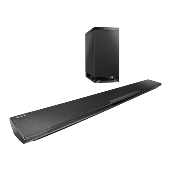
Page 12: Location Of Controls And Components
5 Location of Controls and Components 5.1. Main Unit & Active Subwoofer Key Button Operations Main unit Active subwoofer Standby/on switch ( Select the Bluetooth ® device as the source Press to switch the unit from on to standby NFC touch area mode or vice versa. -
Page 13: Remote Control Key Button Operations
5.2. Remote Control Key Button Operations... -
Page 14: Service Mode
6 Service Mode This unit is equipped with features of service mode mode setting for checking the functions & reliability. 6.1. Service Mode Table 1 Item FL display Key operation Mode name Description Example: Service Mode Upon entering into Service Mode Pressing and hold [VOL-] on main unit then press [▼] follow by [▲] using the remote control. -
Page 15: Service Mode Table
6.2. Service Mode Table 2 Item FL display Key operation Mode name Description Press [VOL+] button 2 times on the Model Name Display the model name Example: remote control. information MODEL: HTB XXX (XXX stand for model number, Eg : 485) Refer to 6.4 for more information The [SVC MODE] display will appear after 3s,... -
Page 16: Service Mode Software Version Check Table
6.3. Service Mode Software Version Check Table Some example of the actual FL display can be found in below table FL Display Position Examples: POS 9 POS 8 POS 7 POS 6 POS 5 POS 4 POS 3 POS 2 POS 1 HTB885 with software version 03 for year 2015... -
Page 17: Service Mode Model Name Display Table
6.4. Service Mode Model Name Display Table FL Display Position Examples: POS 9 POS 8 POS 7 POS 6 POS 5 POS 4 POS 3 POS 2 POS 1 For HTB885 display For HTB485 display 6.5. Service Mode Region Display Table FL Display Position Region Display POS 9... -
Page 18: Service Function Error Code
6.6. Service Function Error Code FL display will also be able to display the Error Code of the respective model indicated in the table below Error Code Description of error Automatic FL Display Diagnostic Contents Example: Abnormality in the stabilized Power Supply Power off the unit during blinking. -
Page 19: Troubleshooting Guide
7 Troubleshooting Guide 7.1. Troubleshooting Flowchart Use the flowchart below to verfiy malfunctions of the unit. 1. Turn on the power of main set. 2. Press and hold the power button for 4 seconds then FL display will show RESET for 2 seconds. 3. -
Page 20: Troubleshooting Guide For Wireless
7.2. Troubleshooting guide for Wireless Sound skip from front speaker (Bluetooth input) Check the radio wave interference of other wireless equipment (cordless phone, Place subwoofer & other wireless equipment more than 2 meters away from main unit Audio confirmation microwave oven, WiFi, other BT devices). No sound from front speaker (Bluetooth input) VFD display BLUETOOTH READY board (Micon/DSP &... -
Page 21: Troubleshooting Guide For Hdmi Module
7.3. Troubleshooting guide for HDMI Module Problems Checking Points Checking components Expected Results 1) No video and audio 1) External Connection checking (Power ON / Standby Pass i) Check whether HDMI Input and Output is reversed. Cable not reverse Through) ii) Check whether HDMI cable properly inserted. - Page 22 1) HDMI audio setting checking (Video is present) i) Check TV Speaker selection setting TV Menu (Viera Menu Link for Panasonic TV) Speaker Selection is set to "TV" (Power ON / Standby Pass ii) Check Player Audio output is set to "ON"...
-
Page 23: Disassembly And Assembly Instructions
8 Disassembly and Assembly Instructions Caution Note: • This section describes the disassembly and/or assembly procedures for all major printed circuit boards & main compo- nents for the unit. (You may refer to the section of “Main components and P.C.B Locations” as described in this service manual) •... -
Page 24: Disassembly Flow Chart
8.2. Disassembly flow chart The following chart is the procedure for disassembling the casing and inside parts for internal inspection when carrying out the ser- vicing. To assemble the unit, reverse the steps shown in the chart below. 8.2.1. Main Speaker Unit (SU-HTB485) 8.2.2. -
Page 25: Types Of Screws
8.3. Types of Screws 8.3.1. Main Speaker Unit (SU-HTB485) 8.3.2. Active Subwoofer (SB-HWA480) -
Page 26: Main Parts Location Diagram
8.4. Main Parts Location Diagram 8.4.1. Main Speaker Unit (SU-HTB485) 8.4.2. Active Subwoofer (SB-HWA480) -
Page 27: Disassembly Of Main Speaker Unit
8.5. Disassembly of Main Speaker Unit 8.5.1. Disassembly of Rear Cabinet Block Step 1 : Remove 18 screws. Step 2 : Lift up Rear Cabinet Block. Caution : Do not exert too much force as it may damage the wiring within. - Page 28 Step 3 : Detach 2P wire at connector (CN6301) on Switch P.C.B.. Step 4 : Remove Acoustic Absorbers. Step 5 : Remove Rear Cabinet Block. 8.5.2. Disassembly of Tilt Switch P.C.B. • Refer to “Disassembly of Rear Cabinet Block”. Step 1 : Remove 2 screws. Step 2 : Remove Tilt Switch P.C.B..
- Page 29 8.5.3. Disassembly of SMPS P.C.B. • Refer to “Disassembly of Rear Cabinet Block”. • Step 1 : Lift up Wire Clamp. Step 2 : Detach 7P wire at connector (CN1) on SMPS P.C.B.. Step 3 : Remove 4 screws. Step 4 : Remove SMPS P.C.B.. 8.5.4.
- Page 30 Step 3 : Remove 1 screw. Step 4 : Lift up Connecting Plate Assembly Unit. Step 5 : Lift up Wire Clamp. Step 6 : Upset Connecting Plate Assembly Unit. Step 7 : Remove 1 screw. Step 8 : Detach 3P wire at connector (CN3301) on Panel P.C.B.. Step 9 : Lift up Panel P.C.B..
- Page 31 Step 10 : Detach 15P FFC at connector (CN3300) on Panel P.C.B.. Step 11 : Remove Panel P.C.B.. 8.5.5. Disassembly of NFC P.C.B. • Refer to “Disassembly of Rear Cabinet Block”. • Refer to (Step 1) - (Step 2) of item 8.5.3. •...
- Page 32 8.5.6. Disassembly of Digital Transmitter Module • Refer to “Disassembly of Rear Cabinet Block”. Step 1 : Remove 1 screw. Step 2 : Detach 24P FFC at connector (CN1) on Digital Transmitter Module. Step 3 : Remove Digital Transmitter Module. 8.5.7.
- Page 33 Step 5 : Remove 2 screws. Step 6 : Remove HDMI P.C.B..
- Page 34 8.5.8. Disassembly of Main P.C.B. • Refer to “Disassembly of Rear Cabinet Block”. • Refer to (Step 1) - (Step 4) of item 8.5.7. Step 1 : Detach 24P FFC at connector (CN2005) on Main P.C.B.. Step 2 : Detach 15P FFC at connector (CN2008) on Main P.C.B.. Step 3 : Detach 5P wire at connector (CN6105) on Main P.C.B..
- Page 35 Step 9 : Slightly lift up Main P.C.B.. Step 10 : Remove Main P.C.B..
- Page 36 Step 11 : Slightly lift up Connecting Plate Assembly Unit. Step 12 : Release Main P.C.B..
- Page 37 Step 13 : Upset Main P.C.B.. Step 14 : Lift up Wire Clamp to release 7P wire. Step 15 : Remove Main P.C.B..
- Page 38 8.5.9. Disassembly of Button P.C.B. • Refer to “Disassembly of Rear Cabinet Block”. Step 1 : Remove 1 screw. Step 2 : Remove Button Holder. Step 3 : Release Button Unit from Front Panel Block. Step 4 : Lift up Button Unit. Step 5 : Detach 3P wire at connector (CN6113) on Button P.C.B..
- Page 39 8.5.10. Disassembly of Woofer Speaker (SP1) • Refer to “Disassembly of Rear Cabinet Block”. Step 1 : Remove 3 screws. Step 2 : Detach speaker wire. Step 3 : Remove Woofer Speaker (SP1). 8.5.11. Disassembly of Woofer Speaker (SP2) • Refer to “Disassembly of Rear Cabinet Block”. Step 1 : Remove 3 screws.
-
Page 40: Disassembly Of Active Subwoofer
8.6. Disassembly of Active Subwoofer 8.6.1. Disassembly of Rear Panel Block Step 3 : Slightly detach Rear Panel Block. Caution : Do not exert too much force as it may damage the wiring inside. Step 1 : Remove 6 screws. Step 4 : Detach 3P Cable Wire at connector (CN1003) on SW DAMP P.C.B.. - Page 41 Step 5 : Detach 2P Wire at connector (CN1005) on SW DAMP 8.6.2. Disassembly of Digital Receiver P.C.B.. Module Step 6 : Remove Rear Panel Block. • Refer to “Disassembly of Rear Panel Block”. Step 1 : Detach 24P FFC at connector (CN1) on Digital Receiver Module.
- Page 42 8.6.3. Disassembly of SW DAMP P.C.B. Step 4 : Remove SW DAMP P.C.B.. • Refer to “Disassembly of Rear Panel Block”. Step 1 : Detach 10P Wire at connector (CN1) on SW SMPS P.C.B.. Step 2 : Detach 4P Cable Wire at connector (CN1002) on the SW DAMP P.C.B..
- Page 43 Step 5 : Detach 24P FFC at connector (CN1) on Digital Step 8 : Remove Digital Receiver Module Unit. Receiver Module. Step 9 : Remove SW DAMP P.C.B.. Step 6 : Upset SW DAMP P.C.B.. Step 7 : Push inward to release catches. 8.6.4.
- Page 44 Step 3 : Press and hold Power Button. 8.6.5. Disassembly of SW SMPS and SW Step 4 : Slightly lift up to remove SW Power Button P.C.B.. AC Inlet P.C.B. • Refer to “Disassembly of Rear Panel Block”. Step 1 : Remove 1 screw. Caution : During assembling, ensure SW Power Button P.C.B.
- Page 45 Step 3 : Detach 10P Wire at connector (CN1) on SW SMPS Caution : During assembling, ensure SW SMPS P.C.B. is seated properly onto the locators of the chassis. P.C.B.. Step 4 : Remove 4 screws. Step 5 : Remove SW SMPS P.C.B. and SW AC Inlet P.C.B..
- Page 46 8.6.6. Disassembly of Bottom Panel 8.6.7. Disassembly of Subwoofer Speaker Assembly (SP61) • Refer to “Disassembly of Bottom Panel Assembly”. Step 1 : Remove 4 screws. Step 2 : Remove Bottom Panel Assembly. Step 1 : Remove 4 screws. Step 2 : Slightly lift up Subwoofer Speaker (SP61). Step 3 : Detach speaker wire at Subwoofer Speaker (SP61).
-
Page 47: Service Position
9 Service Position 9.1. Main Speaker Unit Note: For description of the disassembly procedures, see the Section 8 9.1.1. Checking Tilt Switch P.C.B. Step 1 : Remove Rear Cabinet Block. Step 2 : Remove Tilt Switch P.C.B.. Step 3 : Place the Tilt Switch P.C.B. on an insulated material. Step 4 : Connect 2P wire to connector (CN6301) on Tilt Switch P.C.B.. - Page 48 9.1.3. Checking HDMI P.C.B. • Refer to (Step 1) - (Step 3) of item 9.1.1. Step 1 : Remove 2 screws. Step 2 : Remove 2 screws. Step 3 : Detach 30P FFC at connector (CN1000) on HDMI P.C.B.. Step 4 : Remove HDMI Block. Step 5 : Connect 2P wire to connector (CN6301) on Tilt Switch P.C.B..
- Page 49 9.1.4. Checking Panel P.C.B. & NFC P.C.B. • Refer to (Step 1) - (Step 3) of item 9.1.1. Step 1 : Detach 24P FFC at connector (CN2005) on Main P.C.B.. Step 2 : Detach 15P FFC at connector (CN2008) on Main P.C.B.. Step 3 : Connect 5P wire at connector (CN6105) on Main P.C.B..
- Page 50 Step 7 : Remove 2 screws. Step 8 : Remove 1 screw. Step 9 : Remove Panel P.C.B., Digital Transmitter Module and NFC P.C.B.. Step 10 : Place Main P.C.B. Unit, Connecting Plate Assembly Unit, SMPS P.C.B. Unit, Digital Transmitter Module, Panel P.C.B. and NFC P.C.B.
- Page 51 Step 13 : Place support block at the Front Panel Block. Step 14 : Connect 4P wire to connector (CN5101) on Main P.C.B.. Step 15 : Connect 2P wire to connector (CN5100) on Main P.C.B.. Step 16 : Connect 5P wire to connector (CN6105) on Main P.C.B.. Step 17 : Connect 2P wire to connector (CN6301) on Tilt Switch P.C.B..
- Page 52 9.1.5. Checking Main P.C.B. & Digital Transmitter Module • Refer to (Step 1) - (Step 3) of item 9.1.1. • Refer to (Step 1) - (Step 17) of item 9.1.4. Step 1 : Remove 2 screws. Step 2 : Remove 2 screws. Step 3 : Upset Sub Chassis Unit.
-
Page 53: Active Subwoofer
9.2. Active Subwoofer Note: For description of the disassembly procedures, see the Section 8 9.2.1. Checking SW SMPS & SW DAMP P.C.B. Step 1 : Remove SW DAMP P.C.B.. Step 6 : Connect 3P Wire at connector (CN1003) on SW Step 2 : Remove SW Power Button P.C.B.. -
Page 55: Block Diagram
+13V Q2230 D2231 SWITCH V DET HDMI P.C.B. IC1501 JK1500 C0JBAC000220 OSCILLATOR Ir SYSTEM Q1500 IR BLASTER IR (REMOTE) CN1003 CN1000 IR (REMOTE) CIRCUIT +3.6V NOTE: “ * ” REF IS FOR INDICATION ONLY SC-HTB485EB/EG/GN (SU-HTB485EB/EG/GN) SYSTEM CONTROL BLOCK DIAGRAM... - Page 56 FREQUENCY CIRCUIT WL BCLK CN2005 CN1* WL I2S SCLK CN2005 CN1* WL LRCK WL I2S LRCK CN2005 CN1* WL C SW WL I2S C/SW NOTE: “ * ” REF IS FOR INDICATION ONLY SC-HTB485EB/EG/GN (SU-HTB485EB/EG/GN) HDMI & AUDIO BLOCK DIAGRAM...
- Page 57 FEEDBACK Q5850 D5850 SWITCH IC5701 C0DAAYY00064 SWITCHING REGULATOR CN2004 PCONT PCONT PCON FEEDBACK CIRCUIT CN2004 ECO CTR ECO CTR ECO CTR IC5801 C0DAAYY00072 SHUNT REGULATOR Q5863,Q5873 TO POWER SUPPLY BLOCK (2/2) PRIMARY SECONDARY SC-HTB485EB/EG/GN (SU-HTB485EB/EG/GN) POWER SUPPLY (1/2) BLOCK DIAGRAM...
- Page 58 PW +5V BT SWITCH QR8101 FROM DIGITAL TRANSMITTER MODULE* BT PCON PCON SYSTEM CONTROL CN2005 CN1* REG5V REG5V REG5V 23,24 TO POWER SUPPLY BLOCK (1/2) NOTE: “ * ” REF IS FOR INDICATION ONLY SC-HTB485EB/EG/GN (SU-HTB485EB/EG/GN) POWER SUPPLY (2/2) BLOCK DIAGRAM...
-
Page 59: Active Subwoofer (Sb-Hwa480)
10.2. Active Subwoofer (SB-HWA480) 10.2.1. AUDIO & POWER SUPPLY (1/2) BLOCK DIAGRAM : AUDIO OUTPUT SIGNAL LINE SW SMPS P.C.B. SW DAMP P.C.B. T5701 TRANSFORMER SW AC INLET P.C.B. -23V H1001 -23V -23V P5701 AC INLET L5702 L5703 D5701 IC5203 TH5702 TL11* TL10*... - Page 60 10.2.2. AUDIO & POWER SUPPLY (2/2) BLOCK DIAGRAM : AUDIO OUTPUT SIGNAL LINE SW DAMP P.C.B. SW LED P.C.B. D4001 RED LED CN4000 CN1003 RED LED CN4000 CN1003 GREEN LED GREEN LED IC5200 C1BA00000497 IC3002 POWER AMPLIFIER C0ABBB000244 DIGITAL RECEIVER MODULE* DUAL OP-AMP IC5201...
-
Page 61: Wiring Connection Diagram
Ir SYSTEM DIGITAL (BD/DVD) (TV(ARC)) AUDIO IN (TV) JK2000 PORT CN2006 (FOR SERVICE) (FOR SW DOWNLOADING) SMPS P.C.B. AC IN 220V~240V 50Hz CAUTION RISK OF ELECTRIC SHOCK AC VOLTAGE LINE. PLEASE DO NOT TOUCH THIS P.C.B SC-HTB485EB/EG/GN (SU-HTB485EB/EG/GN) WIRING CONNECTION DIAGRAM... -
Page 62: Active Subwoofer (Sb-Hwa480)
11.2. Active Subwoofer (SB-HWA480) SW POWER BUTTON P.C.B. *CN1004 CN1002 SW LED P.C.B. CN1000 CN4000 SW DAMP P.C.B. CN1005 SUBWOOFER TO DIGITAL RECEIVER MODULE P.C.B. CN1003 H1001 SW AC INLET P.C.B. TL21* (BLK) P5701 AC IN SW SMPS P.C.B. TL20* TL11* 220V~240V 50H z (BLK) -
Page 63: Schematic Diagram
12 Schematic Diagram 12.1. Schematic Diagram Notes • Voltage and signal line (All schematic diagrams may be modified at any time with : +B Signal Line the development of new technology) Notes: : -B Signal Line Main Speaker Unit (SU-HTB485) : HDMI/Optical Audio Input S6101: POWER switch. -
Page 65: Main Speaker Unit (Su-Htb485)
89 90 93 94 97 98 101 102 LB1026 J0JHC0000078 RX1001 D1H81034A042 R1013 R1014 C1027 R1004 4.7K C1028 C1040 LB1017 R1005 4.7K J0JHC0000078 R1010 C1038 R1012 X1000 390K H0J286500042 C1037 HC: HDMI (CONNECTORS): SCHEMATIC DIAGRAM - 3 SC-HTB485EB/EG/GN (SU-HTB485EB/EG/GN) HDMI (MAIN)CIRCUIT... - Page 66 HDMI_FAULT_DET CECIO R1105 C1106 HDMI_+5V_DET HDMI_+5V_DET HDMI_VDD5R6V HDMI_VDD5R6V Q1103 LB1103 C1107 C1108 HDMI_VDD5R6V HDMI_VDD5R6V J0JYC0000366 B1GBCFJJ0048 HDMI_GND HDMI_GND C1115 100P SWITCH HDMI_GND C1109 C1110 C1116 100P LB1104 J0JYC0000366 HC: HDMI (CONNECTORS): SCHEMATIC DIAGRAM - 3 SC-HTB485EB/EG/GN (SU-HTB485EB/EG/GN) HDMI (MAIN) CIRCUIT...
- Page 67 R1210 4.7K PW_BK3R6V R1505 R1208 LB1502 Ir SYSTEM J0JBC0000015 C1501 R1209 IR_GND Q1200 LB1501 Q1500 CECIO J0JCC0000308 B1CFGD000002 R1506 B1ABMF000020 SWITCH LB1500 SWITCH J0JHC0000078 R1507 SC-HTB485EB/EG/GN (SU-HTB485EB/EG/GN) HM: HDMI (MAIN): SCHEMATIC DIAGRAM - 1 ~ 2 R1508 HDMI (CONNECTORS) CIRCUIT...
- Page 68 6800P D2209 100K 150K B0ECKM000008 L2202 G1C150M00023 C2211 C2212 D2202 C2213 SC-HTB485EB/EG/GN (SU-HTB485EB/EG/GN) B0JCPG000032 MAIN (MICON) CIRCUIT DA: MAIN (DAMP): SCHEMATIC DIAGRAM - 6 ~ 7 CO: MAIN (CONNECTOR): SCHEMATIC DIAGRAM - 8 BT: MAIN (BLUETOOTH): SCHEMATIC DIAGRAM - 9...
- Page 69 DC_DET R2018 REMOTE DA: MAIN (DAMP): SCHEMATIC DIAGRAM - 6 ~ 7 ECO_CTR S_DET R2017 CO: MAIN (CONNECTOR): SCHEMATIC DIAGRAM - 8 SD_OUT BT: MAIN (BLUETOOTH): SCHEMATIC DIAGRAM - 9 ECO_CTR R2068 DC_DET DGND PW_FL_WL_5V SC-HTB485EB/EG/GN (SU-HTB485EB/EG/GN) MAIN (MICON) CIRCUIT...
- Page 70 NEGATIVE FEEDBACK HB_HN_3 C5324 1000P HB_LN_3 CN5101 FBN_3_28V FRONT_L- FRONT_L+ TO SPEAKERS TO MAIN (DAMP) CIRCUIT (2/2) MI: MAIN (MICON): SCHEMATIC DIAGRAM - 4 ~ 5 CO: MAIN (CONNECTOR): SCHEMATIC DIAGRAM - 8 C5823 1000P DGND SC-HTB485EB/EG/GN (SU-HTB485EB/EG/GN) MAIN (DAMP) CIRCUIT...
- Page 71 C5316 4.7K 35V470 DGND PW_PVCC_28V R5303 Q5304 B1CZRC000001 PW_PVDD6V NEGATIVE FEEDBACK HB_HN_2 HB_LN_2 MI: MAIN (MICON): SCHEMATIC DIAGRAM - 4 ~ 5 CO: MAIN (CONNECTOR): SCHEMATIC DIAGRAM - 8 FBN_2_28V TO MAIN (DAMP) CIRCUIT (1/2) SC-HTB485EB/EG/GN (SU-HTB485EB/EG/GN) MAIN (DAMP) CIRCUIT...
- Page 72 CIRCUIT (CN6301) PW_3R3V IN SCHEMATIC DIAGRAM - 10 MI: MAIN (MICON): SCHEMATIC DIAGRAM - 4 ~ 5 DA: MAIN (DAMP): SCHEMATIC DIAGRAM - 6 ~ 7 SC-HTB485EB/EG/GN (SU-HTB485EB/EG/GN) MAIN (CONNECTOR) CIRCUIT NOTE: “ * ” REF IS FOR INDICATION ONLY...
- Page 73 BT_HOST_RX KEY1 MAIN (CONNECTOR) RSNE031B0 KEY2 CIRCUIT (CN6105) BLUETOOTH MODULE IN SCHEMATIC DIAGRAM - 8 MI: MAIN (MICON): SCHEMATIC DIAGRAM - 4 ~ 5 SC-HTB485EB/EG/GN (SU-HTB485EB/EG/GN) MAIN (BLUETOOTH) / BUTTON CIRCUIT NOTE: “ * ” REF IS FOR INDICATION ONLY...
- Page 74 R3317 D3306 Q3300 B0ADDH000009 Q3303 B1ABCF000176 B1CFGD000002 SWITCH K100 C3309 LCD DRIVE R3309 C3311 D3307 D3308 B0ADDH000009 Q3301 DZ2J330M0L C3310 B1ADCE000012 D3309 SWITCH R3321 DA2J10100L LB3301 C3301 J0JHC0000107 LB3302 J0JHC0000107 C3300 LB3303 J0JHC0000107 SC-HTB485EB/EG/GN (SU-HTB485EB/EG/GN) PANEL / TILT SWITCH CIRCUIT...
- Page 75 SWITCH Q5761 C5761 K5723...EB/EG/GN C0DAAYY00072 R5761 Q5864 R5829 C5838 B1ABBE000003 PC5760 C5760 R5767 Q5863 6.8K 6.3V470 SHUNT REGULATOR B1ABCF000176 OP-AMP B3PBA0000579 R5869 B1ABCF000176 SWITCH R5865 PCONT R5828 R5817 C5870 R5868 C5828 R5861 C5869 6.3V470 100K 0.01 SC-HTB485EB/EG/GN (SU-HTB485EB/EG/GN) SMPS CIRCUIT...
-
Page 76: Active Subwoofer (Sb-Hwa480)
12.3. Active Subwoofer (SB-HWA480) 12.3.1. SW DAMP CIRCUIT (1/2) SCHEMATIC DIAGRAM - 12 SW DAMP CIRCUIT : +B SIGNAL LINE : -B SIGNAL LINE : AUDIO OUTPUT SIGNAL LINE Q2002 B1AAKD000012 R3107 R3108 R5769 R2000 6.8K 6.8K 1.2K +16V VOLTAGE REGULATOR C2006 R1010 C1016... - Page 77 12.3.2. SW DAMP CIRCUIT (2/2) SCHEMATIC DIAGRAM - 13 SW DAMP CIRCUIT : +B SIGNAL LINE : -B SIGNAL LINE : AUDIO OUTPUT SIGNAL LINE IC5200 C1BA00000497 DIGITAL AMPLIFIER R1015 Q1007 B1ABCF000176 SPEAKER PROTECTION SWITCH C5223 R5206 C5208 C5209 C5212 C5220 C5214 0.47...
- Page 78 12.3.3. SW POWER BUTTON, SW LED & SW AC INLET CIRCUIT SCHEMATIC DIAGRAM - 14 SW POWER BUTTON CIRCUIT SW AC INLET CIRCUIT : +B SIGNAL LINE K5701* K5702* S1000 CN1004* ID SET SW DAMP IDSET P5701 CIRCUIT +5V_GND (RED) T3.15A 250V POWER_SW (CN1002)
- Page 79 12.3.4. SW SMPS CIRCUIT SCHEMATIC DIAGRAM - 15 SW SMPS CIRCUIT : +B SIGNAL LINE ZA1* (HEATSINK) R5857 R5859 QR5867 R5731 B1GBCFJJ0041 R5733 C5730 POWER CONTROL R5855 R5858 PGND 8.2K Q5865 PGND C5863 Q5866 B1ADCE000012 C5862 PVCC B1ABCF000176 SWITCH R5856 PVCC SWITCH DGND...
-
Page 80: Printed Circuit Board
LB1501 LB1502 C1207 R1350 C1206 C1350 LB1352 LB1203 LB1353 R1353 R1601 JK1500 TU1350 TU1200 3634C 3634C JK1601 HDMI AV IN HDMI AV OUT OPTICAL DIGITAL Ir SYSTEM (BD/DVD) (TV(ARC)) AUDIO IN (TV) (SIDE A) (SIDE B) SC-HTB485EB/EG/GN (SU-HTB485EB/EG/GN) HDMI P.C.B. - Page 81 R2019 Q5304 R2002 C2036 C5323 C2011 C5315 C2037 C2010 R5326 C2038 C5324 C5823 C2039 R2035 C2002 Q5303 C5311 R5307 IC2002 C2042 R2055 LB2007 3748AA-1 3748AA-1 (SIDE A) NOTE: " * " REF IS FOR INDICATION ONLY SC-HTB485EB/EG/GN (SU-HTB485EB/EG/GN) MAIN P.C.B.
- Page 82 R5202 D2232 D2211 R5806 D5202 C2234 D2210 Q5804 QR5201 Q5805 PbF 3748AA-1 3748AA-1 Q5803 CN2006 (FOR SW DOWNLOADING) Q5802 USB PORT (FOR SERVICE ONLY) (SIDE B ) NOTE: " * " REF IS FOR INDICATION ONLY SC-HTB485EB/EG/GN (SU-HTB485EB/EG/GN) MAIN P.C.B.
- Page 83 CN3300 C3312 C3311 C4015 LB4015 D3306 D3308 W243 D3307 C3306 W238 W246 Q3301 W230 R3302 C3313 R3305 R3308 R4015 R3301 LB3302 CN3301 FL3300 (TO NFC P.C.B.) LB3301 R3300 R3321 3753AB-1 3753AB-1 SC-HTB485EB/EG/GN (SU-HTB485EB/EG/GN) BUTTON / PANEL / TILT SWITCH P.C.B.
- Page 84 C5760 ZJ5703 R5849 C5761 T3.15A 250V Q5761 Q5851 PC5720 R5761 QR5762 3753AA-1 3753AA-1 CAUTION RISK OF ELECTRIC SHOCK AC VOLTAGE LINE. PLEASE DO NOT TOUCH THIS P.C.B SC-HTB485EB/EG/GN (SU-HTB485EB/EG/GN) NOTE: " * " REF IS FOR INDICATION ONLY SMPS P.C.B.
-
Page 85: Active Subwoofer (Sb-Hwa480)
13.2. Active Subwoofer (SB-HWA480) 13.2.1. SW DAMP, SW POWER BUTTON & SW LED P.C.B. SW DAMP P.C.B. (REP4869BA) Q2002 K1053 Z1002 IC3002 CN1002 R3206 R5783 K1050 C3105 R3204 C3106 R3108 C1005 K1051 W1005 R5769 Q2010 QR2013 R3111 Q1007 TP1* Q5602 C5221 Q2011 C5234... - Page 86 13.2.2. SW SMPS & SW AC INLET P.C.B. SW SMPS P.C.B. (REP4860W) D5803 T5701 SECONDARY PRIMARY (TRANSFORMER) ZJ5701 ZA2* C5712 HEATSINK K5805 C5704 R5703 D5802 TH5860 R5702 C5705 C5808 C5805 L5703 ZA1* HEATSINK C5722 R5733 TL20* (BLK) C5702 D5706 IC5701 R5722 DZ5701 C5700...
-
Page 87: Voltage Measurement
POWER STANDBY IC1000 REF NO. MODE POWER STANDBY IC1000 REF NO. MODE POWER STANDBY IC1000 REF NO. MODE POWER STANDBY IC1000 REF NO. MODE POWER STANDBY IC1100 REF NO. MODE POWER STANDBY REF NO. MODE POWER STANDBY SU-HTB485EB/EG/GN HDMI P.C.B. - Page 88 14.1.2. HDMI P.C.B. (2/2) IC1200 REF NO. MODE POWER STANDBY REF NO. IC1501 MODE POWER STANDBY REF NO. MODE POWER STANDBY SU-HTB485EB/EG/GN HDMI P.C.B.
- Page 89 REF NO. MODE POWER ON STANDBY IC2000 REF NO. MODE POWER ON STANDBY REF NO. IC2001 MODE POWER STANDBY IC2201 REF NO. MODE POWER 29.4 10.1 30.6 STANDBY 29.4 10.1 30.6 IC2202 REF NO. MODE POWER STANDBY SU-HTB485EB/EG/GN MAIN P.C.B.
- Page 90 14.5 30.6 27.8 14.5 30.6 27.8 30.1 STANDBY 14.5 30.6 27.8 14.5 30.6 27.8 30.1 Q5804 Q5805 QR2200 QR2201 QR2202 REF NO. MODE POWER 28.8 28.8 STANDBY 28.8 28.8 QR2303 QR2305 QR5201 REF NO. MODE POWER STANDBY SU-HTB485EB/EG/GN MAIN P.C.B.
- Page 91 14.1.5. PANEL & SMPS P.C.B. IC3300 REF NO. MODE POWER STANDBY REF NO. MODE POWER 12.7 STANDBY 12.7 SU-HTB485EB/EG/GN PANEL P.C.B. IC5701 REF NO. MODE POWER 166.6 14.4 STANDBY 166.6 14.4 IC5801 REF NO. MODE POWER 28.6 STANDBY 16.0 REF NO.
-
Page 92: Active Subwoofer (Sb-Hwa480)
14.2. Active Subwoofer (SB-HWA480) 14.2.1. SW DAMP P.C.B. IC3002 REF NO. MODE POWER -14.2 15.4 STANDBY -14.2 15.4 IC5200 REF NO. MODE CD PLAY 21.8 -22.1 -13.7 22.1 18.3 -22.4 -12.2 -22.4 18.3 22.1 -22.1 -22.1 21.8 STANDBY 21.8 -22.1 -13.7 22.1 18.3 -22.4 -12.2 -22.4 18.3 22.1 -22.1 -22.1 21.8... - Page 93 14.2.2. SW SMPS P.C.B. IC5701 REF NO. MODE POWER 166.6 14.4 STANDBY 166.6 14.4 IC5801 REF NO. MODE POWER 16.0 STANDBY 16.0 IC5822 REF NO. MODE POWER STANDBY Q5720 Q5760 Q5761 Q5865 Q5866 REF NO. MODE CD PLAY 20.6 21.0 20.0 20.0 20.0 20.0...
-
Page 95: Exploded View And Replacement Parts List
15 Exploded View and Replacement Parts List 15.1. Cabinet Parts Location-1 (SU-HTB485) *HEATSINK T5701 TU1350 P5701 (SMPS P.C.B.) TU1200 (HDMI P.C.B.) JK1601 JK2000 JK1500 ZJ5703 CN2006 CN1000 CN5101 **IC2002 (EEPROM IC) CN2005 *HEATSINK CN2008 CN6105 (BLUETOOTH CN1003 P.C.B.) CN2004 CN5100 **(MAIN P.C.B.) (DIGITAL TRANSMITTER MODULE) -
Page 96: Cabinet Parts Location-2 (Su-Htb485)
15.2. Cabinet Parts Location-2 (SU-HTB485) (TILT SWITCH P.C.B.) CN6301 S6302 SU-HTB485EBK SU-HTB485EGK SU-HTB485GNK NOTE: " * " PART IS NOT SUPPLIED / REF IS FOR INDICATION ONLY. CABINET DRAWING... -
Page 97: Cabinet Parts Location (Sb-Hwa480)
15.3. Cabinet Parts Location (SB-HWA480) *CN1004 (SW POWER BUTTON P.C.B.) S1001 S1000 *HEAT SINK CN1002 (SW DAMP P.C.B.) ZJ1002 *(SW LED P.C.B.) CN1005 *CN4000 ZJ1001 CN1003 CN1000 H1001 ZJ1003 IC5200 (DIGITAL RECEIVER MODULE) P5701 *TL21 (BLK) (SW AC INLET *TL11 P.C.B.) (RED) ZJ5703... -
Page 98: Packaging (Sc-Htb485)
15.4. Packaging (SC-HTB485) ACCESSORIES BAG REMOTE CONTROL SU-HTB485EB/EG/GN A2 x 2 AC CORD (FOR GN ONLY) A2 x 2 AC CORD (FOR EG ONLY) OI BOOK A2 x 2 AC CORD (FOR EB ONLY) IR BLASTER SB-HWA480EB/GN WALL MOUNT BRACKET... -
Page 99: Mechanical Replacement Parts List
15.5. Mechanical Replacement Parts List 15.5.1. Main Speaker Unit Safety Ref. Part No. Part Name & QTY Remarks Description (SU-HTB485) RMF0681 EPT SEALER RMF0682 EPT SEALER RMF0684 EPT SEALER Safety Ref. Part No. Part Name & QTY Remarks RMF0698 CHASSIS CUSHION Description RMK0872 MAIN CHASSIS... - Page 100 15.5.3. Packaging & Accessories Safety Ref. Part No. Part Name & QTY Remarks Description (SC-HTB485) L0AA06A00103 WOOFER SPEAKER (6CM) 15.5.2. Active Subwoofer Safety Ref. Part No. Part Name & QTY Remarks Description (SB-HWA480) PACKING MATERIALS RPG0Q40-1 PACKING CASE(SC) Safety Ref. Part No.
-
Page 101: Electrical Replacement Parts List
15.6. Electrical Replacement Parts List 15.6.1. Main Speaker Unit Safety Ref. Part No. Part Name & QTY Remarks Description (SU-HTB485) IC2001 RFKWFTB485EM IC W/DATA (E.S.D) JIGS&AD IC2002 RFKV5044QC IC W/DATA (E.S.D) Safety Ref. Part No. Part Name & QTY Remarks JIGS&AD Description IC2002... - Page 102 Safety Ref. Part No. Part Name & QTY Remarks Safety Ref. Part No. Part Name & QTY Remarks Description Description Q5401 B1ABDF000033 TRANSISTOR (E.S.D) D5710 DA2J10100L DIODE (E.S.D) Q5402 B1ABDF000033 TRANSISTOR (E.S.D) D5712 B0EAMM000057 DIODE (E.S.D) Q5403 B1CZRC000001 TRANSISTOR (E.S.D) D5713 DZ2J330M0L DIODE...
- Page 103 Safety Ref. Part No. Part Name & QTY Remarks Safety Ref. Part No. Part Name & QTY Remarks Description Description LB1353 J0JCC0000042 INDUCTOR LB1500 J0JHC0000078 INDUCTOR CHIP JUMPERS LB1501 J0JCC0000308 INDUCTOR LB1502 J0JBC0000015 INDUCTOR K100 D0GBR00J0004 0 1/10W LB1600 J0JBC0000014 INDUCTOR K201 D0GBR00J0004 0 1/10W...
- Page 104 Safety Ref. Part No. Part Name & QTY Remarks Safety Ref. Part No. Part Name & QTY Remarks Description Description R1205 D0GA473JA023 47K 1/16W R2231 D0GB102JA065 1K 1/10W R1206 D0GA103JA023 10K 1/16W R2232 D0GB104JA065 100K 1/10W R1207 D0GA101JA023 100 1/16W R2233 D0GB103JA065 10K 1/10W...
- Page 105 Safety Ref. Part No. Part Name & QTY Remarks Safety Ref. Part No. Part Name & QTY Remarks Description Description R5438 D0GFR10ZA043 10 1/4W RX2002 D1H83304A042 RESISTOR NETWORK R5513 D0GB104JA065 100K 1/10W RX2003 D1H83304A042 RESISTOR NETWORK R5514 D0GB104JA065 100K 1/10W RX2004 D1H83304A042 RESISTOR NETWORK R5535...
- Page 106 Safety Ref. Part No. Part Name & QTY Remarks Safety Ref. Part No. Part Name & QTY Remarks Description Description C1103 F1G1A1040006 0.1uF C2043 F1G1C104A149 0.1uF C1104 F1J1A106A043 10uF C2044 F1G1A1040006 0.1uF C1105 F1G1A1040006 0.1uF C2046 F1G1H680A541 68pF C1106 F1G0J1050007 1uF 6.3V C2049 F1H0J4750004 4.7uF...
- Page 107 15.6.2. Active Subwoofer Safety Ref. Part No. Part Name & QTY Remarks Description (SB-HWA480) C5325 F1K1H105A250 1uF C5401 F1H1H104B047 0.1uF C5402 F1H1H104B047 0.1uF Safety Ref. Part No. Part Name & QTY Remarks C5403 F1H1H104B047 0.1uF Description C5404 F1H1H104B047 0.1uF C5405 F1G1E1040001 0.1uF PRINTED CIRCUITS C5406...
- Page 108 Safety Ref. Part No. Part Name & QTY Remarks Safety Ref. Part No. Part Name & QTY Remarks Description Description SWITCHES RESISTORS S1000 EVQ21405R SW I/D SET R1007 D0GB103JA065 10K 1/10W S1001 K0F122B00107 SW POWER R1008 D0GB103JA065 10K 1/10W R1009 D0GB472JA065 4.7K 1/10W CONNECTORS...
- Page 109 Safety Ref. Part No. Part Name & QTY Remarks Safety Ref. Part No. Part Name & QTY Remarks Description Description R5802 ERJ3RBD223V 1/16W C5240 F2A1J470A050 47uF R5804 ERJ3RED154V 150K 1/16W C5522 F1H1H104B047 0.1uF R5805 D1BB1002A074 10K 1/10W C5523 F1H1H104B047 0.1uF R5806 D0GB103JA065 10K 1/10W...