Sony CAS-1 Service Manual
Compact audio system, compact audio amplifier
Hide thumbs
Also See for CAS-1:
- Operating instructions manual (60 pages) ,
- Manual (36 pages) ,
- Precautions/troubleshooting (32 pages)
Table of Contents
Advertisement
SERVICE MANUAL
Ver. 1.2 2016.04
Note:
Be sure to keep your PC used for service and
checking of this unit always updated with the
latest version of your anti-virus software.
In case a virus affected unit was found during
service, contact your Service Headquarters.
COMPONENT MODEL NAME
Compact Audio Amplifi er
Speaker System
• Please refer to service manual separately issued for Speaker System.
(US, CND only)
AUDIO POWER SPECIFICATIONS
POWER OUTPUT AND TOTAL HARMONIC DISTORTION:
With 5 ohm loads, both channels driven, from 20 - 20,000 Hz; rated 20
watts per channel minimum RMS power, with no more than 10% total
harmonic distortion from 250 milliwatts to rated output.
Amplifier section
Reference Power Output
24 W + 24 W (5 Ω, 1 kHz, THD 10%)
Rated Power Output
20 W + 20 W (5 Ω, 20 Hz - 20 kHz, THD 1%)
Speaker impedance match
5 Ω - 16 Ω
Frequency response
10 Hz - 40 kHz (+0 dB, –3 dB) (5 Ω,
B (USB-B) input)
BLUETOOTH section
Output
BLUETOOTH Specification Power Class 2
Maximum communication range
Line of sight approx. 10 m*
1
Available pairing
Up to 9 devices
When the unit has been already been paired with 9 BLUETOOTH
devices and you attempt to pair with an additional device, the pairing
information of the oldest connected device is deleted automatically.
Radio frequency
2.4 GHz band (2.4000 GHz - 2.4835 GHz)
Communication System
BLUETOOTH Specification Version 3.0
Compatible BLUETOOTH Profiles*
2
A2DP (Advanced Audio Distribution Profile)
AVRCP (Audio Video Remote Control Profile)
3
Supported codec*
SBC*
4
AAC*
5
6
LDAC*
Supported content protection method
SCMS-T method
Transmission bandwidth (A2DP)
20 Hz - 20,000 Hz (with 44.1 kHz sampling)
20 Hz - 40,000 Hz (with LDAC 96 kHz sampling, 990 kbps)
*
1
The actual range will vary depending on factors such as obstacles
between devices, magnetic fields around a microwave oven, static
electricity, reception sensitivity, aerial's performance, operating system,
software application, etc.
2
*
BLUETOOTH standard profiles indicate the purpose of BLUETOOTH
communication between devices.
*
3
Codec: Audio signal compression and conversion format
*
4
Subband Codec
*
5
Advanced Audio Coding
9-896-223-03
Sony Video & Sound Products Inc.
2016D33-1
©
2016.04
Published by Sony Techno Create Corporation
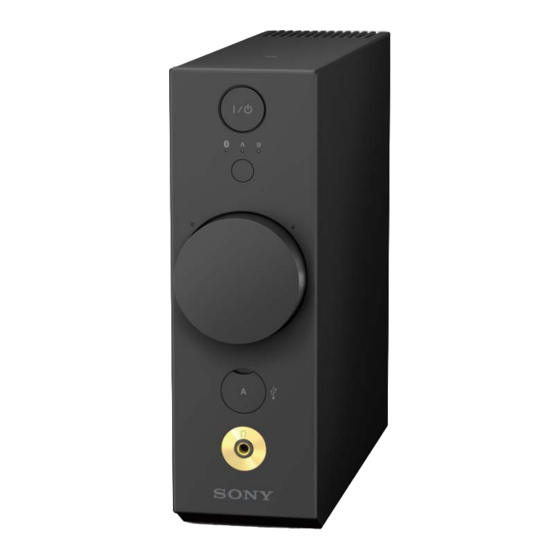
Photo: TA-CA1
CAS-1
TA-CA1
SS-HW5
SPECIFICATIONS
*
6
LDAC is an audio coding technology developed by Sony that enables
the transmission of High-Resolution (Hi-Res) Audio content, even over
a BLUETOOTH connection. Unlike other BLUETOOTH compatible coding
technologies such as SBC, it operates without any down-conversion of
the Hi-Res Audio content*
7
, and allows approximately three times more
data*
8
than those other technologies to be transmitted over a
BLUETOOTH wireless network with unprecedented sound quality, by
means of efficient coding and optimized packetization.
*
7
Excluding DSD format contents
*
8
In comparison with SBC (Subband Coding) when the bitrate of 990 kbps
(96/48 kHz) or 909 kbps (88.2/44.1 kHz) is selected.
USB port section
A (USB-A) port
You can connect a USB flash drive and Walkman that is compatible with
this unit.
Supported format*
1
MP3: 16/22.05/24/32/44.1/48 kHz, 32 - 320 kbps (CBR/VBR)
AAC: 16/22.05/24/32/44.1/48/88.2/96 kHz, 40 - 320 kbps (CBR/VBR)
WMA: 32/44.1/48 kHz, 16 - 320 kbps (CBR/VBR)
WAV: 16/22.05/24/32/44.1/48/88.2/96/176.4/192 kHz (16/24 bit)
AIFF: 32/44.1/48/88.2/96/176.4/192 kHz (16/24 bit)
FLAC: 44.1/48/88.2/96/176.4/192 kHz (16/24 bit)
ALAC: 44.1/48/88.2/96/176.4/192 kHz (16/24 bit)
DSD (DSF/DSDIFF): 2.8 MHz (1 bit)
Transfer speed
High-speed
Supported USB device
Mass Storage Class (MSC)
Maximum output current
1A MAX
Depending on the device, the charge current might be limited to
500 mA.
Supported file system
FAT
FAT32
exFAT
B (USB-B) port
You can connect a compatible device such as a PC, etc., to this
unit using the supplied USB cable.
1
Supported format*
PCM: 44.1/48/88.2/96/176.4/192 kHz (16/24/32 bit)
DSD (DSF/DSDIFF): 2.8 MHz (1 bit)
1
*
Compatibility with all encoding/writing software, recording
devices and recording media cannot be guaranteed.
CAS-1
Canadian Model
Chinese Model
Hong Kong Model
Singapore Model
Malaysia Model
Taiwan Model
Korean Model
Headphones section
250 mW + 250 mW (8 Ω, THD 1%)
180 mW + 180 mW (32 Ω, THD 1%)
35 mW + 35 mW (300 Ω, THD 1%)
General
Power requirements
DC 19.5 V (using the supplied AC adaptor connected to AC 100 V-240
V, 50 Hz/60 Hz power supply)
Power consumption (using the supplied AC adaptor)
29 W
Power consumption (during standby mode)
0.5 W (When BLUETOOTH standby mode is set to off.)
2 W (When BLUETOOTH standby mode is set to on.)
Dimensions (w/h/d) (including projecting parts)
Approx. 55 mm × 178 mm × 210 mm (2
Mass
7
/
oz)
Approx. 1.3 kg (2 Ib 13
8
Supplied accessories
AC adapter (1)
AC cord (mains lead) (1) (CEL)
AC cord (1) (Except CEL)
USB cable (1)
Speaker cord (2)
Spike (Large) (4)
Speaker base (2)
Remote control (1)
Operating Instructions (1)
Precautions / Troubleshooting (1)
Warranty (1) (US, CND, CEL, CH, KR only)
Stand (1)
Flyer (Stand) (1)
Flyer (Spike) (1)
Design and specifications are subject to change without notice.
COMPACT AUDIO SYSTEM
COMPACT AUDIO AMPLIFIER
TA-CA1
US Model
AEP Model
UK Model
Thai Model
1
/
inches × 7
1
/
inches × 8
3
/
inches)
4
8
8
CAS-1
TA-CA1
Advertisement
Table of Contents

Related Manuals for Sony CAS-1


Summary of Contents for Sony CAS-1
- Page 1 • Please refer to service manual separately issued for Speaker System. SPECIFICATIONS (US, CND only) LDAC is an audio coding technology developed by Sony that enables Headphones section AUDIO POWER SPECIFICATIONS the transmission of High-Resolution (Hi-Res) Audio content, even over 250 mW + 250 mW (8 Ω, THD 1%)
- Page 2 United States and in other countries. WT-540A. Follow the manufacturers’ instructions to use these The BLUETOOTH® word mark and logos are registered trademarks owned by BLUETOOTH SIG, Inc. and any use of such marks by Sony Corporation instruments. is under license.
-
Page 3: Table Of Contents
CAS-1 Ver. 1.2 TABLE OF CONTENTS SERVICING NOTES 5-4. Printed Wiring Boards - MAIN Section - ....... 39 ..........5-5. Schematic Diagram - MAIN Section (1/5) - ....40 5-6. Schematic Diagram - MAIN Section (2/5) - ....41 DISASSEMBLY 5-7. -
Page 4: Servicing Notes
CAS-1 Ver. 1.2 SECTION 1 SERVICING NOTES The SERVICING NOTES contains important information for servicing. Be sure to read this section before repairing the unit. UNLEADED SOLDER CAPACITOR ELECTRICAL DISCHARGE PROCESSING Boards requiring use of unleaded solder are printed with the lead- When checking the board, for the electric shock prevention, con- free mark (LF) indicating the solder contains no lead. - Page 5 “Walkman”, smartphone and so on corresponding to this unit, and check the operation of playback, charge and so on. For each operation checks, download the following software from the support web site and so on of Sony system stereo as necessary, and use them. •...
- Page 6 CAS-1 WRITING OPERATION OF SERIAL NUMBER AFTER 4. Check the serial number 7 digits on the serial/mode label stuck on the bottom side of this unit. REPLACING THE MAIN BOARD Be sure to perform the writing operation of serial number accord-...
- Page 7 CAS-1 BOND FIXATION OF ELECTRICAL PARTS When C265 on the AMP board replaced, fi x the parts by using the bond (UB510G) (Refer to the fi gure below). – AMP Board (Component Side) – C265 Bond (UB510G) LED INDICATOR The unit uses LED to inform you of the volume level, the mute status and so on (Refer to the fi gure table).
-
Page 8: Disassembly
CAS-1 SECTION 2 DISASSEMBLY • This set can be disassembled in the order shown below. 2-1. DISASSEMBLY FLOW 2-2. PANEL_BOTTOM 2-18. SERVICE POSITION (Page 9) (Page 23) 2-3. COVER_PANEL_BACK (Page 9) 2-4. PANEL_CASE BLOCK (Page 10) 2-6. AMP BOARD-1 2-5. NFC MODULE (NFC1) 2-17. - Page 9 CAS-1 Ver. 1.1 Note: Follow the disassembly procedure in the numerical order given. 2-2. PANEL_BOTTOM 2 four screws 1 four cushion_foot (P 3 Note 2: Insert a utility knife etc. in the ditch then remove the cushion_foot. When remove the cushion_foot with a finger, the adhesive surface and the rubber on the back will away.
-
Page 10: Panel_Case Block
CAS-1 2-4. PANEL_CASE BLOCK top side rear side 1 four screws (BVTP 3 Note: When removing these screws, use the long screwdriver more than 15 cm. 15 cm or more bottom side six claws 2 Slide the panel_case block to remove the... -
Page 11: Nfc Module (Nfc1)
CAS-1 2-5. NFC MODULE (NFC1) 3 NFC module (NFC1) terminal side 2 Insert the tweezers or flat stick in the notch of the base_NFC, and lift the NFC module carefully to peel off the adhesive (NFC). 1 flexible flat cable (6 pin) -
Page 12: Amp Board-1
CAS-1 2-6. AMP BOARD-1 • Continued on 2-7 (page 13). 1 screw (BVTP 3 Note: Please be careful to forget remove the screw. bottom side top side 1 two screws (BVTP 3 rear side 2 four screws (BVTP 3 top side... -
Page 13: B To B Board, Amp Board-2
CAS-1 Ver. 1.1 2-7. B TO B BOARD, AMP BOARD-2 Note 1: When installing the B TO B board, align white mark of the MAIN board and B TO B board. 2 screw (BVTP 2.6) B TO B board 1 four screws... -
Page 14: Front Panel Block-1
CAS-1 2-8. FRONT PANEL BLOCK-1 • Continued on 2-9 (page 15). 2 LED board cable connector (CN657) 1 HP board cable connector (CN400) 3 USB board cable connector top side (CN663) stand etc. rear side 4 DC fan cable connector... -
Page 15: Front Panel Block-2
CAS-1 Ver. 1.1 2-9. FRONT PANEL BLOCK-2 top side 2 Remove the main chassis block 5 front panel block in the direction of the arrow. 3 Draw out the HP board cable and LED board cable from the hole. panel_origin... -
Page 16: Vol Board, Led Board, Button (Power Ir), Indicator (Vol)
CAS-1 2-11. VOL BOARD, LED BOARD, BUTTON (POWER IR), INDICATOR (VOL) top side LED board cable 2 nut coating clip 1 knob vol assy side rear side VOL board LED board 3 Remove the wire from the coating clip. top side 4 Draw out the VOL board block from the hole. -
Page 17: Hp Board, Usb Board
CAS-1 2-12. HP BOARD, USB BOARD top side rear side front panel assy 5 GND plate (USB) 6 connector (CN162) 7 USB board 4 two screws (B 3 2 connector (CN161) 3 HP board 1 two screws (B 3... -
Page 18: Bluetooth Module (Bt1)
CAS-1 2-13. BLUETOOTH MODULE (BT1) Flexible flat cable (FFC1) setting 3 screw bluetooth module (BT1) (BVTP 3 rear side terminal face 2 connector terminal filament tape face (sub material) top side CN654 MAIN board 1 filament tape (sub material) front side... -
Page 19: Network Board
CAS-1 2-14. NETWORK BOARD 1 three screws (BVTP 2.6) 3 heatsink_BRD_MTK block 2 Remove the heatsink_BRD_MTK block in the direction of the arrow. duct (MTK) Note on the installing the heatsink_BRD_MTK block heatsink_BRD_MTK top side duct (MTK) notch notch rear side... -
Page 20: Main Board-1
CAS-1 2-15. MAIN BOARD-1 • Continued on 2-16 (page 21). Flexible flat cable (FFC2) setting 1 two filament tapes Flexible flat cable (FFC1) setting (sub material) 2 connector (CN654) Terminal face is CN655 below side. MAIN board 3 Flexible flat cable (FFC2) -
Page 21: Main Board-2
CAS-1 Ver. 1.1 2-16. MAIN BOARD-2 Note 1: When the MAIN board is replaced, refer to “WRITING OPERA- TION OF SERIAL NUMBER AFTER REPLACING THE MAIN BOARD” on page 6. Note 2: The MAIN board has been changed in the midway of production. -
Page 22: Panel_Case
CAS-1 2-17. PANEL_CASE 2 acoustic absorbent (case) 1 Hi-Res label rear side (50 12 mm)(Thickness: 4 mm) front side front 1 mm side 5 damper (case) (130 20 mm) 3 mm 2 acoustic absorbent (case) 3 acoustic absorbent (case) (50 12 mm)(Thickness: 4 mm) -
Page 23: Service Position
CAS-1 2-18. SERVICE POSITION AMP board stand (notebook, etc.) AMP board junction jig Note: Refer to “JIG” ET004 on page 5. alligator clip cord alligator clip cord chassis MAIN board stand (notebook, etc.) -
Page 24: Test Mode
CAS-1 SECTION 3 TEST MODE Preparation: FIRMWARE VERSION DISPLAY Use the following remote commander for test mode of this unit. It can check the fi rmware version of system controller, NET- Note 1: It cannot operation the test mode with the remote commander of WORK board and BLUETOOTH module. - Page 25 CAS-1 LED CHECK FAN TEST It can check the lighting-up of each LEDs. It can check the operation of fan motor. (Refer to “LED position” on page 24 about position of LED) Procedure: Procedure: 1. Enter the servicing mode. 1. Enter the servicing mode.
- Page 26 CAS-1 TEMPERATURE SENSOR TEST SETTING ALL RESET It can check the operation of temperature sensor. It can delete the setting contents. (Refer to “LED position” on page 24 about position of LED) (Refer to “LED position” on page 24 about position of LED)
- Page 27 CAS-1 HISTORY MODE Status indicator LED Numeral It can check the history information at the last time of protect error of volume ● ● ● ● ● ● ● that occurred. ○ ● ● ● ● ● ● (Refer to “LED position” on page 24 about position of LED) ●...
- Page 28 CAS-1 TEST TONE It can output the test tone (1 kHz). Procedure: 1. Enter the servicing mode. (Refer to “1. Setting method of servicing mode” on page 24) 2. Press the buttons on the remote commander that correspond to each test tone modes in order, and transmit the test code to the main unit (Refer to the following table).
-
Page 29: Troubleshooting
CAS-1 SECTION 4 TROUBLESHOOTING 1. Power does not turn on Power does not turn on. DC +19.5 V is outputted from the AC Replace the AC adaptor. adaptor. Fuse (F001) on the AMP board does Replace the fuse (F001) on the AMP not blow. - Page 30 CAS-1 2. Sound is not outputted from the headphone Note: Perform the operation check in the dotted line frame in the state of connecting the Sound is not outputted from the headphone to this unit. headphone. (Except for parts replacement and so on)
- Page 31 CAS-1 3. Sound is not outputted from the speaker Note: Perform the operation check in the dotted line frame in the state of connecting the Sound is not outputted from the speaker. speakers of both left and right to this unit.
- Page 32 CAS-1 4. The protection feature is activated The protection feature is activated. The protection feature display is not Remove the foreign matter from the appeared, when turning the power on main unit, then turn the power on The foreign matter is mixed into the...
- Page 33 If you connect the PC to the B (USB-B) port on the rear side of the unit, make sure the dedicated driver is installed to the PC. Check that the sound device setting of your computer is set to “Sony Audio.” If not, set it correctly.
- Page 34 CAS-1 MEMO...
-
Page 35: Diagrams
CAS-1 SECTION 5 DIAGRAMS 5-1. BLOCK DIAGRAM - AUDIO INPUT Section - CN160 USB SWITCH AUDIO DSP, SYSTEM CONTROLLER AUDIO SWITCH IC900 IC652 (1/3) IC656 NETWORK BOARD DAC-DATA, DAC-BCK, DAC-LRCK DAC-DATA >001B (Page 36) 8 D+ USB1_D+ I2S_DATA_O 28 AUDIO-DIN3... -
Page 36: Block Diagram - Amp Section
CAS-1 5-2. BLOCK DIAGRAM - AMP Section - AUDIO CODEC DIGITAL POWER AMP DAMP-DATA, IC210 IC204 DAMP-BCK, TB200 L224 DAMP-LRCK DAMP-DATA (Page 35) >002B 1 SDIN1 PWMOUT1PR 8 PWM_B OUT_B DAMP-BCK L223 56 BCKI DAMP-LRCK – 55 LRCKI PWMOUT1NR 6 PWM_A... -
Page 37: Block Diagram - Panel/Power Supply Section
CAS-1 5-3. BLOCK DIAGRAM - PANEL/POWER SUPPLY Section - +12V +12V REGULATOR IC205 DIGITAL POTENTIOMETER AUDIO DSP, SYSTEM CONTROLLER REGULATOR PVDD IC652 (3/3) IC215 Q211 – 215, 217, (FOR DIGITAL POWER AMP) HOKUTO-SDA, Q220, 221, 226 HOKUTO-SCL HOKUTO-SDA SHUNT >003B... - Page 38 CAS-1 Ver. 1.2 THIS NOTE IS COMMON FOR PRINTED WIRING BOARDS AND SCHEMATIC DIAGRAMS. • Circuit Boards Location (In addition to this, the necessary note is printed in each block.) For Printed Wiring Boards. For Schematic Diagrams. BLUETOOTH module Note:...
-
Page 39: Printed Wiring Boards - Main Section
CAS-1 Ver. 1.2 5-4. PRINTED WIRING BOARDS - MAIN Section - • See page 38 for Circuit Boards Location. • : Uses unleaded solder. (Page 45) (Page 46) (Page 52) (Page 45) HP BOARD B TO B BOARD LED BOARD USB BOARD >04P... -
Page 40: Schematic Diagram - Main Section (1/5)
CAS-1 Ver. 1.1 5-5. SCHEMATIC DIAGRAM - MAIN Section (1/5) - • See page 54 for IC Block Diagrams. NETWORK MAIN BOARD (1/5) BOARD CN900 R907 3.3V 3.3V 4.7k JL906 R925 I2C_SDA I2S_MCK_O R908 4.7k JL907 JL933 MTK-A-BUSY I2C_SCL Reserved(BUSY_I) -
Page 41: Schematic Diagram - Main Section (2/5)
CAS-1 Ver. 1.1 5-6. SCHEMATIC DIAGRAM - MAIN Section (2/5) - • See page 52 for Waveforms. • See page 54 for IC Block Diagrams. MAIN BOARD (2/5) CN653 JL662 R804 JL663 DEBUG-TXD DEBUG-RXD R805 JL664 R806 JL693 NSRST NSRST... -
Page 42: Schematic Diagram - Main Section (3/5)
CAS-1 Ver. 1.2 5-7. SCHEMATIC DIAGRAM - MAIN Section (3/5) - • See page 54 for IC Block Diagrams. MAIN BOARD (3/5) (US, CND, CH, TW, TH) C480 470p R413 ET402 R486 D402 1SS362-TE85L C420 C478 270p 1000p R434 (CHASSIS) -
Page 43: Schematic Diagram - Main Section (4/5)
CAS-1 Ver. 1.1 5-8. SCHEMATIC DIAGRAM - MAIN Section (4/5) - • See page 58 for IC Pin Function Description. MAIN BOARD (4/5) >011S MTK-3.3V-EN MAIN MTK-1.5V-EN BOARD MTK-3.3V-STBY-EN (5/5) (Page 44) R700 C686 C687 C690 C692 C749 R802 C684... -
Page 44: Schematic Diagram - Main Section (5/5)
CAS-1 Ver. 1.1 5-9. SCHEMATIC DIAGRAM - MAIN Section (5/5) - • See page 54 for IC Block Diagrams. MAIN BOARD (5/5) IC553 +1.5V REGULATOR IC553 S-13A1A15-E6T1U3 C571 0.001 CL554 ON/OFF R564 VSS_5 VSS_2 JL553 VOUT C565 C583 C577 R568... -
Page 45: Printed Wiring Boards - Usb/Hp Boards
CAS-1 Ver. 1.2 5-10. PRINTED WIRING BOARDS - USB/HP Boards - • See page 38 for Circuit Boards Location. 5-11. SCHEMATIC DIAGRAM - USB/HP Boards - • : Uses unleaded solder. USB BOARD USB BOARD USB BOARD (COMPONENT SIDE) (CONDUCTOR SIDE) -
Page 46: Printed Wiring Board - B To B Board
CAS-1 Ver. 1.2 5-12. PRINTED WIRING BOARD - B TO B Board - • See page 38 for Circuit Boards Location. 5-13. SCHEMATIC DIAGRAM - B TO B Board - • : Uses unleaded solder. (Page 41) (Page 47) B TO B BOARD... -
Page 47: Schematic Diagram - Amp Board (1/3)
CAS-1 Ver. 1.2 5-14. SCHEMATIC DIAGRAM - AMP Board (1/3) - • See page 54 for IC Block Diagrams. • See page 58 for IC Pin Function Description. AMP BOARD (1/3) C347 C235 C279 C280 C281 C381 1000p FB011 100V... -
Page 48: Schematic Diagram - Amp Board (2/3)
CAS-1 Ver. 1.1 5-15. SCHEMATIC DIAGRAM - AMP Board (2/3) - • See page 54 for IC Block Diagrams. AMP BOARD (2/3) Q208 C252 2SC2713G-TE85L 470p C299 VDD DETECT 100V 2200p R239 (Type-12) C286 C398 C309 C273 D224 D223 C274... -
Page 49: Schematic Diagram - Amp Board (3/3)
CAS-1 Ver. 1.1 5-16. SCHEMATIC DIAGRAM - AMP Board (3/3) - • See page 52 for Waveforms. • See page 54 for IC Block Diagrams. AMP BOARD (3/3) F001 D010 JL013 250V 1SR154-400TE-25 >023S JL012 19V_PVDD JL011 J001 PVDD_GND R032 DC IN 19.5V... -
Page 50: Printed Wiring Board - Amp Board (Type-11: Us, Canadian, Chinese, Taiwan, Thai Models)
CAS-1 Ver. 1.2 5-17. PRINTED WIRING BOARD - AMP Board (Type-11: US, Canadian, Chinese, Taiwan, Thai models) - • See page 38 for Circuit Boards Location. • : Uses unleaded solder. B TO B BOARD (Page 46) >05P AMP BOARD... -
Page 51: Printed Wiring Board - Amp Board (Type-12)
CAS-1 Ver. 1.2 5-18. PRINTED WIRING BOARD - AMP Board (Type-12) - • See page 38 for Circuit Boards Location. • : Uses unleaded solder. B TO B BOARD (Page 46) >06P AMP BOARD CN1101 AMP BOARD (COMPONENT SIDE) (CONDUCTOR SIDE) -
Page 52: Printed Wiring Boards - Vol/Led Boards
CAS-1 Ver. 1.2 • Waveforms 5-19. PRINTED WIRING BOARDS - VOL/LED Boards - • See page 38 for Circuit Boards Location. • : Uses unleaded solder. – MAIN Board – – AMP Board – IC657 3 (A2) IC659 2 IC002 8 (PH) -
Page 53: Schematic Diagram - Vol/Led Boards
CAS-1 Ver. 1.2 5-20. SCHEMATIC DIAGRAM - VOL/LED Boards - • See page 54 for IC Block Diagrams. LED BOARD D101 - 107 (STATUS INDICATOR) C101 C102 C103 C104 C105 C106 C107 C121 C122 D101 D102 D103 D104 D105 D106... - Page 54 CAS-1 • IC Block Diagrams IC553 S-13A1A15-E6T1U3 IC554 S-13A1A18-E6T1U3 – MAIN Board – IC555 S-13A1A12-E6T1U3 IC401 PCM1795DBR IC556 – 558 S-13A1A33-E6T1U3 IC654 BU4229F-TR VCC2L GND 1 VOUT 1 ZEROL 1 ZERO AGND3L VREF ZEROR 2 DETECT CURRENT OVERCURRENT IOUTL– SEGMENT...
- Page 55 CAS-1 – AMP Board – IC001 TPS5420DRG4 GATE DRIVE BOOT 1 N.C. 2 SHDN SHDN N.C. 3 1.221 V SLOW VREF HICCUP BANDGAP START BOOT REFERENCE REGULATOR SHDN SHDN SHDN BOOT RAMP OVERCURRENT OSCILLATOR GENERATOR PROTECTION SHDN HICCUP SHDN SHDN...
- Page 56 CAS-1 IC204 CXD9981TN GVDD_B /DTW UNDER- VOLTAGE INTERNAL PULLUP PROTECTION RESISTORS TO VREG PROTECTION TEMP. SENSE I/O LOGIC GVDD_A BST_A PVDD_A PVDD_A GATE PWM_A TIMING CTRL OUT_A RCV. DRIVE BTL/PBTL-CONFIGURATION PULLDOWN RESISTOR /RESET_AB GND_A GND_B BTL/PBTL-CONFIGURATION PULLDOWN RESISTOR GATE TIMING...
- Page 57 CAS-1 IC211 TC74VHC74FT (EK) IC215 ISL22317UFRTZ-TK 13 12 11 SCL 1 POWER-UP, SDA 2 INTERFACE, EEPROM A1 3 CONTROL REF_A 4 LOGIC REF_B 5 6 GND 1 2 3 4 5 6 – LED Board – IC101 TC62D748CFNAG IC104 MM1839A33NRE...
- Page 58 CAS-1 • IC Pin Function Description MAIN BOARD IC652 R7S7200052CFP (AUDIO DSP, SYSTEM CONTROLLER) Pin No. Pin Name Description VBUS-OVR-DET VBUS over current detection signal input terminal “L”: over current DAC-ZERO-DATA Zero data fl ag input from the D/A converter “H”: zero data...
- Page 59 CAS-1 Pin No. Pin Name Description LED-BRIGHT White LED brightness control signal output terminal “L”: dark, “H”: bright LEDDRV-SCK Serial data transfer clock signal output to the LED driver N.C. Not used XPROTECTOR Protect signal input from the speaker amplifi er section “L”: protect...
- Page 60 CAS-1 Pin No. Pin Name Description OPWRSB_3.3V +3.3V power on/off control signal output terminal for NETWORK board “H”: power on LED-POWER-RED Not used LED-POWER-GREEN Not used Ground terminal Power on/off control signal output terminal for VBUS and fan motor to the DC/DC converter FUSB_DCDC_EN “H”: power on...
- Page 61 CAS-1 Pin No. Pin Name Description SF-SO Serial data input from the serial fl ash HP-GAIN PHONES GAIN switch input terminal “L”: LOW, “H”: HI PVcc Power supply terminal (+3.3V) BT-RESET Reset signal output to the BLUETOOTH module “L”: reset...
- Page 62 CAS-1 AMP BOARD IC210 CXD3776ER-T9 (AUDIO CODEC) Pin No. Pin Name Description SDIN1 Audio signal input from the audio DSP SDIN2 Audio signal input terminal Not used LRCKO L/R sampling clock signal input/output terminal Not used BCKO Bit clock signal input/output terminal...
-
Page 63: Exploded Views
CAS-1 Ver. 1.2 SECTION 6 EXPLODED VIEWS Note: • -XX and -X mean standardized parts, so • The mechanical parts with no reference • Color variations they may have some difference from the number in the exploded views are not sup- Black : US, CND, CEL, CH, KR, TH models original one. -
Page 64: Amp Board Section
CAS-1 Ver. 1.2 6-2. AMP BOARD SECTION • Rear view NFC1 not supplied supplied not supplied FFC2 front panel section TB200 MAIN board section AMP board (CEL) (See Note) supplied with TB200 supplied with TB201 TB201 not supplied not supplied not supplied Note: When the complete AMP board (Ref. -
Page 65: Main Board Section
CAS-1 Ver. 1.2 6-3. MAIN BOARD SECTION • Rear view FFC1 not supplied not supplied supplied not supplied not supplied MAIN board not supplied not supplied not supplied not supplied not supplied not supplied Note 1: When the complete MAIN board (Ref. No. 104) is replaced, Note 2: The MAIN board has been changed in the midway of produc- refer to “WRITING OPERATION OF SERIAL NUMBER AF-... -
Page 66: Front Panel Section
CAS-1 Ver. 1.2 6-4. FRONT PANEL SECTION • Rear view not supplied not supplied supplied with EN190 not supplied not supplied supplied not supplied EN190 (USB board) not supplied not supplied (VOL board) not supplied (HP board) not supplied not supplied not supplied Ref. -
Page 67: Panel Case Section
CAS-1 Ver. 1.2 6-5. PANEL CASE SECTION Ref. No. Part No. Description Remark Ref. No. Part No. Description Remark 4-582-201-01 DAMPER (CASE) (size: 130X20 mm) 4-582-202-11 ABSORBENT (CASE), ACOUSTIC 4-582-202-01 ABSORBENT (CASE), ACOUSTIC (size: 50X12X1 mm) (size: 50X12X4 mm) 4-566-988-01... -
Page 68: Electrical Parts List
CAS-1 Ver. 1.2 SECTION 7 ELECTRICAL PARTS LIST Note: • Due to standardization, replacements in • CAPACITORS When indicating parts by reference num- uF: μF the parts list may be different from the ber, please include the board name. parts specifi ed in the diagrams or the com- •... - Page 69 CAS-1 Ver. 1.2 Ref. No. Part No. Description Remark Ref. No. Part No. Description Remark C237 1-118-039-11 CERAMIC CHIP 1uF C296 1-118-361-11 CERAMIC CHIP 0.1uF C238 1-118-039-11 CERAMIC CHIP 1uF C297 1-118-361-11 CERAMIC CHIP 0.1uF C239 1-118-039-11 CERAMIC CHIP 1uF...
- Page 70 CAS-1 Ver. 1.1 Ref. No. Part No. Description Remark Ref. No. Part No. Description Remark < CONNECTOR > IC006 6-718-108-01 IC KIA7907F-RTF/P CN003 (Not supplied) CONNECTOR, BOARD TO BOARD 60P IC204 6-714-477-01 IC CXD9981TN (See Note) IC205 6-717-953-01 IC SI-3010KM-TLA...
- Page 71 CAS-1 Ver. 1.2 Ref. No. Part No. Description Remark Ref. No. Part No. Description Remark R016 1-218-871-11 METAL CHIP 0.5% 1/10W R256 1-216-857-11 METAL CHIP 1/10W R017 1-218-847-11 METAL CHIP 0.5% 1/10W R257 1-216-857-11 METAL CHIP 1/10W R018 1-218-839-11 METAL CHIP 0.5%...
- Page 72 CAS-1 Ver. 1.2 B TO B Ref. No. Part No. Description Remark Ref. No. Part No. Description Remark < TERMINAL > < CAPACITOR > TB200 1-854-057-11 TERMINAL BOARD, SPEAKER 2P (without CAP) C101 1-118-361-11 CERAMIC CHIP 0.1uF (SPEAKERS 5 ~ 16 L) (US, CND, CH, TW, TH)
- Page 73 CAS-1 Ver. 1.2 MAIN Ref. No. Part No. Description Remark Ref. No. Part No. Description Remark R109 1-216-805-11 METAL CHIP 1/10W C423 1-118-290-11 CERAMIC CHIP 0.001uF R111 1-216-805-11 METAL CHIP 1/10W C424 1-118-290-11 CERAMIC CHIP 0.001uF R112 1-216-805-11 METAL CHIP...
- Page 74 CAS-1 MAIN Ref. No. Part No. Description Remark Ref. No. Part No. Description Remark C570 1-118-041-11 CERAMIC CHIP 4.7uF C697 1-118-391-11 CERAMIC CHIP 0.01uF C571 1-118-403-11 CERAMIC CHIP 0.001uF C698 1-118-417-11 CERAMIC CHIP 0.1uF C572 1-118-403-11 CERAMIC CHIP 0.001uF C699...
- Page 75 CAS-1 MAIN Ref. No. Part No. Description Remark Ref. No. Part No. Description Remark C917 1-118-289-11 CERAMIC CHIP 0.1uF IC551 6-718-379-01 IC RP108J081D-FE < CONNECTOR > IC553 6-721-865-01 IC S-13A1A15-E6T1U3 IC554 6-719-013-01 IC S-13A1A18-E6T1U3 CN400 1-764-250-21 PIN, CONNECTOR (PC BOARD) 4P...
- Page 76 CAS-1 MAIN Ref. No. Part No. Description Remark Ref. No. Part No. Description Remark R436 1-250-793-11 METAL CHIP 220K 1/8W R656 1-218-941-81 METAL CHIP 1/16W R437 1-250-793-11 METAL CHIP 220K 1/8W R657 1-218-941-81 METAL CHIP 1/16W R438 1-216-833-11 METAL CHIP...
- Page 77 CAS-1 MAIN Ref. No. Part No. Description Remark Ref. No. Part No. Description Remark R722 1-218-941-81 METAL CHIP 1/16W R785 1-218-943-11 METAL CHIP 1/16W R723 1-218-941-81 METAL CHIP 1/16W R786 1-218-933-11 METAL CHIP 1/16W R724 1-218-957-11 METAL CHIP 2.2K 1/16W...
- Page 78 CAS-1 MAIN NETWORK Ref. No. Part No. Description Remark Ref. No. Part No. Description Remark R849 1-216-295-91 SHORT CHIP R929 1-218-961-11 METAL CHIP 4.7K 1/16W R851 1-218-969-11 METAL CHIP 1/16W R930 1-218-961-11 METAL CHIP 4.7K 1/16W R852 1-218-990-81 SHORT CHIP...
- Page 79 CAS-1 Ver. 1.2 Ref. No. Part No. Description Remark D171 6-502-967-01 DIODE DZ2J06200L < EARTH TERMINAL > ET160 1-780-482-11 EARTH TERMINAL < JUMPER RESISTOR > R162 1-216-864-91 SHORT CHIP R163 1-216-864-91 SHORT CHIP ************************************************************* VOL BOARD ********** < CAPACITOR >...
- Page 80 CAS-1 Ver. 1.2 Ref. No. Part No. Description Remark ACCESSORIES ************ AC adapter (1) Remote control (1) 4-572-691-33 MANUAL, INSTRUCTION (TRADITIONAL CHINESE) (TW) 4-572-691-82 MANUAL, INSTRUCTION (KOREAN) (KR for White) 4-572-692-11 REFERENCE GUIDE (ENGLISH, FRENCH) (US, CND) 4-572-692-22 REFERENCE GUIDE (ENGLISH) (CEL)
- Page 81 CAS-1 TA-CA1 US Model Canadian Model SERVICE MANUAL AEP Model UK Model Chinese Model Ver. 1.2 2016.04 Hong Kong Model Singapore Model Malaysia Model Taiwan Model SUPPLEMENT-1 Korean Model Thai Model File this supplement with the service manual. Subject: Change of MAIN board (Suffi x-12) The MAIN board has been changed in the midway of production.
- Page 82 CAS-1 Ver. 1.2 1. NOTE OF REPLACING THE AMP OR MAIN BOARDS The AMP board (US, Canadian, Chinese, Taiwan and Thai models) • Change of AMP Board (All Destination Common) has been changed in the midway of production and MAIN board It is possible to directly replace, even if the boards of any type are has been changed in the midway of production.
- Page 83 CAS-1 If the new MAIN board for replacing is the Type-12: • Change of MAIN Board (CEL and Korean models only) • If both of AMP/MAIN boards that are installed to the unit to If the new MAIN board for replacing is the Type-11: perform the repair have been the Type-11 •...
- Page 84 CAS-1 2. DIAGRAMS THIS NOTE IS COMMON FOR PRINTED WIRING BOARDS AND SCHEMATIC DIAGRAMS. (In addition to this, the necessary note is printed in each block.) For Printed Wiring Boards. For Schematic Diagrams. Note: Note: • All capacitors are in μF unless otherwise noted. (p: pF) 50 •...
- Page 85 CAS-1 Ver. 1.2 2-1. PRINTED WIRING BOARD - MAIN Board - • : Uses unleaded solder. Refer to page Refer to page Refer to page Refer to page HP BOARD B TO B BOARD LED BOARD USB BOARD >04P >02P >03P...
- Page 86 CAS-1 2-2. SCHEMATIC DIAGRAM - MAIN Board (1/5) - Refer to page 40 on original service manual NETWORK MAIN BOARD (1/5) BOARD CN900 R907 3.3V 3.3V 4.7k JL906 R925 I2C_SDA I2S_MCK_O R908 4.7k JL907 JL933 MTK-A-BUSY I2C_SCL Reserved(BUSY_I) R918 JL923...
- Page 87 CAS-1 Ver. 1.2 2-3. SCHEMATIC DIAGRAM - MAIN Board (2/5) - MAIN BOARD (2/5) R804 JL663 DEBUG-TXD DEBUG-RXD R805 JL664 R806 JL693 NSRST R807 JL694 R808 JL695 R809 JL699 R810 JL700 C728 R826 JL701 TRST 4700p R851 JL702 >005S C737...
- Page 88 CAS-1 2-4. SCHEMATIC DIAGRAM - MAIN board (3/5) - MAIN BOARD (3/5) C479 COM400 0.0022 R413 ET402 R486 D402 1SS362-TE85L C420 C446 270p 2200p R434 (CHASSIS) CL435 C444 CL431 C447 R422 C435 C436 R424 R435 0.0022 1000p 100V D401 1SS362-TE85L...
- Page 89 CAS-1 Ver. 1.2 2-5. SCHEMATIC DIAGRAM - MAIN Board (4/5) - MAIN BOARD (4/5) >011S MTK-3.3V-EN MTK-1.5V-EN MAIN BOARD MTK-3.3V-STBY-EN (5/5) (Page 10) R700 C686 C687 C690 C692 C749 R802 C684 C700 C696 C693 C697 100p 0.01 0.01 100k 100p 100p 0.01...
- Page 90 CAS-1 2-6. SCHEMATIC DIAGRAM - MAIN Board (5/5) - MAIN BOARD (5/5) IC553 +1.5V REGULATOR IC553 S-13A1A15-E6T1U3 C571 0.001 CL554 ON/OFF R564 VSS_5 VSS_2 JL553 VOUT C565 C583 C577 R568 1000p 100V IC551 R562 +3.3V REGULATOR 4.7k IC554 IC551 RP108J081D-FE VDD_1.5V_MTK...
- Page 91 CAS-1 Ver. 1.2 MAIN 3. ELECTRICAL PARTS LIST Note: • Due to standardization, replacements in • CAPACITORS • Abbreviations the parts list may be different from the uF: μF : European, East European, Hong parts specifi ed in the diagrams or the com- •...
- Page 92 CAS-1 Ver. 1.2 MAIN Ref. No. Part No. Description Remark Ref. No. Part No. Description Remark C576 1-118-403-11 CERAMIC CHIP 0.001uF C707 1-118-417-11 CERAMIC CHIP 0.1uF C577 1-100-158-91 CERAMIC CHIP 1000PF 100V C708 1-118-391-11 CERAMIC CHIP 0.01uF C578 1-100-158-91 CERAMIC CHIP 1000PF...
- Page 93 CAS-1 MAIN Ref. No. Part No. Description Remark Ref. No. Part No. Description Remark CN657 1-816-113-21 CONNECTOR 15P IC652 (Not supplied) IC R7S7200052CFP (See Note) CN663 1-770-469-21 PIN, CONNECTOR (PC BOARD) 2P IC654 6-719-856-01 IC BU4229F-TR CN666 (Not supplied) CONNECTOR, BOARD TO BOARD 60P...
- Page 94 CAS-1 MAIN Ref. No. Part No. Description Remark Ref. No. Part No. Description Remark R459 1-250-785-11 METAL CHIP 100K 1/8W R664 1-218-933-11 METAL CHIP 1/16W R460 1-250-785-11 METAL CHIP 100K 1/8W R665 1-218-965-11 METAL CHIP 1/16W R461 1-250-761-11 METAL CHIP...
- Page 95 CAS-1 MAIN Ref. No. Part No. Description Remark Ref. No. Part No. Description Remark R730 1-218-941-81 METAL CHIP 1/16W R794 1-218-933-11 METAL CHIP 1/16W R731 1-218-965-11 METAL CHIP 1/16W R795 1-218-933-11 METAL CHIP 1/16W R732 1-218-941-81 METAL CHIP 1/16W R798...
- Page 96 CAS-1 MAIN Ref. No. Part No. Description Remark Ref. No. Part No. Description Remark R869 1-216-295-91 SHORT CHIP R937 1-218-990-81 SHORT CHIP R870 1-218-990-81 SHORT CHIP R938 1-218-990-81 SHORT CHIP R871 1-218-990-81 SHORT CHIP R940 1-218-941-81 METAL CHIP 1/16W R872...
- Page 97 CAS-1 MEMO...
- Page 98 CAS-1 REVISION HISTORY Ver. Date Description of Revision 2015.10 2015.11 Addition of Chinese, Taiwan and Korean models Deletion of Australian model Addition of note of screw tightening torque for the cover_panel_back Addition of note of screw tightening torque for the DC fan (M1) Change of AMP, B TO B, HP, LED, USB and VOL boards (Except CEL and Korean models) (Suffi...