Table of Contents
Advertisement
Advertisement
Table of Contents

Related Manuals for Clevo N141ZU


Summary of Contents for Clevo N141ZU
- Page 1 N141ZU...
- Page 3 Preface Notebook Computer N141ZU Service Manual...
- Page 4 Preface Notice The company reserves the right to revise this publication or to change its contents without notice. Information contained herein is for reference only and does not constitute a commitment on the part of the manufacturer or any subsequent ven- dor.
- Page 5 This manual is intended for service personnel who have completed sufficient training to undertake the maintenance and inspection of personal computers. It is organized to allow you to look up basic information for servicing and/or upgrading components of the N141ZU se- ries notebook PC.
- Page 6 Preface IMPORTANT SAFETY INSTRUCTIONS Follow basic safety precautions, including those listed below, to reduce the risk of fire, electric shock and injury to per- sons when using any electrical equipment: 1. Do not use this product near water, for example near a bath tub, wash bowl, kitchen sink or laundry tub, in a wet basement or near a swimming pool.
- Page 7 Preface Instructions for Care and Operation The notebook computer is quite rugged, but it can be damaged. To prevent this, follow these suggestions: Don’t drop it, or expose it to shock. If the computer falls, the case and the components could be damaged. Do not expose the computer Do not place it on an unstable Do not place anything heavy...
- Page 8 Preface Avoid interference. Keep the computer away from high capacity transformers, electric motors, and other strong mag- netic fields. These can hinder proper performance and damage your data. Take care when using peripheral devices. Use only approved brands of Unplug the power cord before peripherals.
- Page 9 Preface Battery Precautions • Only use batteries designed for this computer. The wrong battery type may explode, leak or damage the computer. • Do not continue to use a battery that has been dropped, or that appears damaged (e.g. bent or twisted) in any way. Even if the computer continues to work with a damaged battery in place, it may cause circuit damage, which may possibly result in fire.
- Page 10 Preface Related Documents You may also need to consult the following manual for additional information: User’s Manual on CD/DVD This describes the notebook PC’s features and the procedures for operating the computer and its ROM-based setup pro- gram. It also describes the installation and operation of the utility programs provided with the notebook PC. System Startup °...
-
Page 11: Table Of Contents
Preface Contents Introduction ..........1-1 Top (without Fingerprint) .............. A-4 Bottom ................... A-5 Overview ..................1-1 LCD ....................A-6 Specifications ..................1-2 MB ....................A-7 External Locator - Top View with LCD Panel Open ......1-4 Schematic Diagrams......... B-1 External Locator - Front & Right Side Views .........1-5 External Locator - Left Side &... - Page 12 Preface KBC ITE IT8587 ................B-27 WLAN/BT, 4G ................B-28 M Key PCIE SSD ................. B-29 SATA, LED, LID, SW ..............B-30 USB / TPM ................... B-31 Conn, CCD, Fan, TP, LED KB ............ B-32 3V, 5V, 3VS, 5VS, 1.8VS CTL ........... B-33 VDD3, VDD5 ................
-
Page 13: Introduction
Chapter 1: Introduction Overview This manual covers the information you need to service or upgrade the N141ZU series notebook computer. Information about operating the computer (e.g. getting started, and the Setup utility) is in the User’s Manual. Information about dri- vers (e.g. -
Page 14: Specifications
Introduction Specifications Processor Options Video Adapter Intel® Core™ i7 Processor Intel UHD Graphics 620 i7-8565U (1.80GHz) Dynamic Frequency 8MB Smart Cache, 14nm, DDR4-2400MHz, TDP 15W Intel Dynamic Video Memory Technology Intel® Core™ i5 Processor Microsoft DirectX® 12 Compatible Latest Specification Information i5-8265U (1.60GHz) Pointing Device 6MB Smart Cache, 14nm, DDR4-2400MHz, TDP 15W... - Page 15 Introduction Card Reader Communication Embedded Multi-In-1 Card Reader Built-In 10/100/1000Mb Base-TX Ethernet LAN MMC (MultiMedia Card) / RS MMC 1.0M HD PC Camera Module SD (Secure Digital) / Mini SD / SDHC/ SDXC (Factory Option) Windows Hello Camera Module Interface (Factory Option) 4G M.2 Module One USB 3.1 Gen 2 Type-C Port* WLAN/ Bluetooth M.2 Modules:...
-
Page 16: External Locator - Top View With Lcd Panel Open
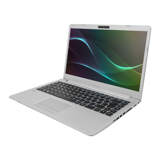
Introduction External Locator - Top View with LCD Panel Open Figure 1 Top View 1. PC Camera 2. *PC Camera LED *When the PC camera is in use, the LED will be illuminated in white. 3. Built-In Microphone 4. LCD 5. -
Page 17: External Locator - Front & Right Side Views
Introduction External Locator - Front & Right Side Views Figure 2 Front View 1. LED Indicator FRONT VIEW Figure 3 Right Side View 1. USB 3.0 (USB 3.1 Gen 2) Type-C Port RIGHT SIDE VIEW (Factory Option) Thunderbolt 3 Combo Port (Type- 2. -
Page 18: External Locator - Left Side & Rear View
Introduction External Locator - Left Side & Rear View Figure 4 Left Side View 1. DC-In Jack 2. USIM Card Reader (for 3G/4G LEFT SIDE VIEW USIM Cards) - Factory Option 3. USB 3.0 (USB 3.1 Gen 1) Type-A Port 4. -
Page 19: External Locator - Bottom View
Introduction External Locator - Bottom View Figure 6 Bottom View 1. Vent 2. Speakers Overheating To prevent your com- puter from overhea- ting, make sure no- thing blocks any vent while the computer is in use. External Locator - Bottom View 1 - 7... -
Page 20: Mainboard Overview - Top (Key Parts)
Introduction Mainboard Overview - Top (Key Parts) Figure 7 Mainboard Top Key Parts 1 - 8 Mainboard Overview - Top (Key Parts) -
Page 21: Mainboard Overview - Bottom (Key Parts)
Introduction Mainboard Overview - Bottom (Key Parts) Figure 8 Mainboard Bottom Key Parts 1. CPU 2. Memory Slots DDR4 SO-DIMM 3. KBC-ITE IT8587 Mainboard Overview - Bottom (Key Parts) 1 - 9... -
Page 22: Mainboard Overview - Top (Connectors)
Introduction Mainboard Overview - Top (Connectors) Figure 9 Mainboard Top Connectors 1. USB Board Connector 2. Keyboard Cable Connector 3. White LED Keyboard Connector 4. RJ-45 LAN Jack 5. HDMI-Out Port 6. Mini Display Port 7. USB Port 3.0/3.1 Type A Port 8. -
Page 23: Mainboard Overview - Bottom (Connectors)
Introduction Mainboard Overview - Bottom (Connectors) Figure 10 Mainboard Bottom Connectors 1. Multi-in-1 Card Reader 2. Fan Connector 3. LCD Cable Connector 4. Speaker Connector 5. HDD Connector 6. Battery Connector 7. M.2 Card Connector (SSD) 8. 3G/4G Connector 9. WLAN Connector 10. - Page 24 Introduction 1 - 12...
-
Page 25: Disassembly
Chapter 2: Disassembly Overview This chapter provides step-by-step instructions for disassembling the N141ZU series notebook’s parts and subsystems. When it comes to reassembly, reverse the procedures (unless otherwise indicated). We suggest you completely review any procedure before you take the computer apart. -
Page 26: Maintenance Tools
Disassembly NOTE: All disassembly procedures assume that the system is turned OFF, and disconnected from any power supply (the battery is removed too). Maintenance Tools The following tools are recommended when working on the notebook PC: • M3 Philips-head screwdriver •... -
Page 27: Maintenance Precautions
Disassembly Maintenance Precautions The following precautions are a reminder. To avoid personal injury or damage to the computer while performing a removal and/or replacement job, take the following precautions: Power Safety Don't drop it. Perform your repairs and/or upgrades on a stable surface. If the computer falls, the case and other components Warning could be damaged. -
Page 28: Disassembly Steps
Disassembly Disassembly Steps The following table lists the disassembly steps, and on which page to find the related information. PLEASE PERFORM THE DISASSEMBLY STEPS IN THE ORDER INDICATED. To remove the Keyboard: To remove and install the M.2 SSD Module: 1. -
Page 29: Removing The Keyboard
Disassembly Removing the Keyboard Figure 1 1. Turn off the computer, turn it over. Keyboard Removal 2. Remove screws from the bottom case (Figure 1a). 3. Open it up with the LCD on a flat surface before pressing at point to release the keyboard module (use the spe- cific eject stick to do this) while releasing the keyboard in the direction of the arrow... -
Page 30: Removing The Battery
Disassembly Removing the Battery Figure 2 Battery Removal 1. Turn off the computer, turn it over to remove the keyboard (page 2 - 2. Remove screws (Figure 2a). a. Remove the screws. 3. Remove screws on the bottom case (Figure 2b). -
Page 31: Removing The Hard Disk Drive
Disassembly Removing the Hard Disk Drive Figure 3 HDD Assembly The hard disk drive can be taken out to accommodate other 2.5" serial (SATA) hard disk drives with a height of 7.0mm Removal (h). Follow your operating system’s installation instructions, and install all necessary drivers and utilities (as outlined in Chapter 4 of the User’s Manual) when setting up a new hard disk. - Page 32 Disassembly 4. Slightly lift to pull the hard disk assembly in the direction of arrow (Figure 4c Figure 4 5. Lift the hard disk out of the bay (Figure 4d HDD Assembly 6. Reverse the process to install a new hard disk (do not forget to replace all the screws and bottom cover). Removal (cont’d.) c.
-
Page 33: Removing The System Memory (Ram)
Disassembly Removing the System Memory (RAM) Figure 5 RAM Module The computer has two memory sockets for 260 pin Small Outline Dual In-line Memory Modules (SO-DIMM) supporting Removal DDR4 2133MHz. The main memory can be expanded up to 32GB. The total memory size is automatically detected by the POST routine once you turn on your computer. - Page 34 Disassembly 5. Pull the latches to release the second module if necessary. 6. Insert a new module holding it at about a 30° angle and fit the connectors firmly into the memory slot. 7. The module will only fit one way as defined by its pin alignment. Make sure the module is seated as far into the slot as it will go.
-
Page 35: Removing The Wireless Lan Module
Disassembly Removing the Wireless LAN Module Figure 6 Wireless LAN 1. Turn off the computer, turn it over to remove the keyboard (page 2 - 5) and battery (page 2 - Module Removal 2. The Wireless LAN module will be visible at point on the mainboard (Figure 6a). -
Page 36: Wireless Lan, And Combo Module Cables
Disassembly Wireless LAN, and Combo Module Cables Note that the cables for connecting to the antennae on WLAN, WLAN & Bluetooth Combo, 3G and LTE modules are not labelled. The cables/covers (each cable will have either a black or transparent cable cover) are color coded for iden- tification as outlined in the table below. -
Page 37: Removing The 3G Module
Disassembly Removing the 3G Module Figure 7 3G Module Removal Procedure 3G Module Removal 1. Turn off the computer, turn it over to remove the keyboard (page 2 - 5) and battery (page 2 - a. Locate the module. 2. Locate the module, it is visible at point Figure 7a b. -
Page 38: Removing And Installing The M.2 Ssd Module
Disassembly Removing and Installing the M.2 SSD Module Figure 8 M.2 SSD-1 Module M.2 SSD-1 Removal Procedure Removal 1. Turn off the computer, turn it over to remove the keyboard (page 2 - 5) and battery (page 2 - 2. The M.2 SSD module will be visible at point on the mainboard (Figure 8a). - Page 39 Disassembly M.2 SSD-2 Removal Procedure Figure 9 1. Turn off the computer, turn it over to remove the keyboard (page 2 - 5) and battery (page 2 - M.2 SSD-2 Module 2. The M.2 SSD module will be visible at point on the mainboard (Figure 9a).
- Page 40 Disassembly M.2 SSD Installation Procedure Figure 10 M.2 SSD Module 1. Place the thermal pad on the module as shown (Figure 10a). Installation 2. Insert the module in the computer Figure 10b 3. Tighten the screw to secure the module in place (Figure 10c) a.
-
Page 41: Removing The Ccd
Disassembly Removing the CCD Figure 11 CCD Removal 1. Turn off the computer, turn it over to remove the keyboard (page 2 - 5) and battery (page 2 - 2. Lift up the inner frame and run your fingers around the inner frame of the LCD panel at the points as indicated by a. - Page 42 Disassembly 4. Disconnect the cable (Figure 12c). Figure 12 5. Remove the CCD module (Figure 12d). CCD Removal 6. Reverse the process to install a new CCD module. (cont’d.) c. Disconnect the cable. d. Remove the CCD mod- ule. 7.
-
Page 43: Part Lists
Appendix A:Part Lists This appendix breaks down the N141ZU series notebook’s construction into a series of illustrations. The component part numbers are indicated in the tables opposite the drawings. Note: This section indicates the manufacturer’s part numbers. Your organization may use a different system, so be sure to cross-check any relevant documentation. -
Page 44: Part List Illustration Location
Part List Illustration Location The following table indicates where to find the appropriate part list illustration. Table A - 1 Part List Illustration Part Location page A - 3 Top (with Fingerprint) Top (without Fingerprint) page A - 4 page A - 5 Bottom page A - 6 page A - 7... -
Page 45: Top (With Fingerprint
Top (with Fingerprint) Figure A - 1 (with Fingerprint) Top (with Fingerprint) A - 3... -
Page 46: Top (Without Fingerprint
Top (without Fingerprint) Figure A - 2 (without Finger- print) A - 4 Top (without Fingerprint) -
Page 47: Bottom
Bottom Figure A - 3 Bottom Bottom A - 5... -
Page 48: Lcd
Figure A - 4 A - 6 LCD... - Page 49 Figure A - 5 MB A - 7...
- Page 50 A - 8...
-
Page 51: Schematic Diagrams
Schematic Diagrams Appendix B: Schematic Diagrams This appendix has circuit diagrams of the N141ZU notebook’s PCB’s. The following table indicates where to find the appropriate schematic diagram. Diagram - Page Diagram - Page Diagram - Page Table B - 1... - Page 52 Schematic Diagrams System Block Diagram 6 IN 1 6-7P-N13Z6-003 N130/140 ZU Whiskey LAKE U42 (HDCP2.2) System Block Diagram MAIN BOARD SHEET 1~40 6-71-N13Z0-D02A USB BOARD 3V,5V,3VS,5VS 1866/ 2133 MHz 6-71-N13Z3-D01 SHEET 41 DDR4 SHEET 32 DDR4 AUDIO BOARD SO-DIMM A SHEET 16 HDMI SYSTEM SMBUS...
- Page 53 Schematic Diagrams Processor 1/12 M_A_DQ[63:0] M_B_DQ[63:0] U24B U24C M_A_CLK_DDR#0 DDR0_CKN_0/DDR0_CKN_0 M_A_DQ0 M_B_DQ0 AF28 M_A_CLK_DDR0 M_B_CLK_DDR#0 DDR0_DQ_0/DDR0_DQ_0 DDR0_CKP_0/DDR0_CKP_0 DDR1_DQ_0/DDR0_DQ_16 DDR1_CKN_0/DDR1_CKN_0 M_A_DQ1 M_B_DQ1 AF29 DDR0_DQ_1/DDR0_DQ_1 DDR0_CKN_1/DDR0_CKN_1 M_A_CLK_DDR#1 DDR1_DQ_1/DDR0_DQ_17 DDR1_CKP_0/DDR1_CKP_0 M_B_CLK_DDR0 M_A_DQ2 M_B_DQ2 AE28 M_A_CLK_DDR1 M_B_CLK_DDR#1 DDR0_DQ_2/DDR0_DQ_2 DDR0_CKP_1/DDR0_CKP_1 DDR1_DQ_2/DDR0_DQ_18 DDR1_CKN_1/DDR1_CKN_1 M_A_DQ3 M_B_DQ3 AE29 M_B_CLK_DDR1 DDR0_DQ_3/DDR0_DQ_3 DDR1_DQ_3/DDR0_DQ_19...
- Page 54 Schematic Diagrams Processor 2/12 U24A DDI TO mDP/TBT PORT EDP PANEL 18,19 MDP_D#0 DDI1_TXN_0 EDP_TXN_0 EDP_TXN_0 18,19 MDP_D0 DDI1_TXP_0 EDP_TXP_0 EDP_TXP_0 18,19 MDP_D#1 DDI1_TXN_1 EDP_TXN_1 EDP_TXN_1 18,19 MDP_D1 DDI1_TXP_1 EDP_TXP_1 EDP_TXP_1 DIFF=85ohm, 18,19 MDP_D#2 EDP_TXN_2 DDI1_TXN_2 EDP_TXN_2 18,19 MDP_D2 DDI1_TXP_2 EDP_TXP_2 EDP_TXP_2 DIFF=85ohm...
-
Page 55: Processor 11/12
Schematic Diagrams Processor 3/12 VCCIO 150_04 U24Q WHL QS/CFL/WHL_ES1_CNL U CFG0 CFG_0 RSVD_TP_5 1K_04 CFG0 RSVD_TP_6 CFG_1 CP36 CFG_2 IST_TRIG CFG3 CN36 CFG_3 RSVD_TP_12 CFG4 CFG_4 1K_04 R470 CFG4 CFG5 BJ36 CFG_5 RSVD_TP_3/RSVD/RSVD_TP_3 CFG6 BJ34 CFG_6 RSVD_TP_4/RSVD/RSVD_TP_4 CFG7 CFG_7 BK34 *1K_04 R469 CFG6... - Page 56 Schematic Diagrams Processor 4/12 Sheet 5 of 45 VDD3 SPI_3.3V W /O TPM R673 0_04 3.3VA Processor 4/12 W /TPM R674 0_04 D02 CHANGE POWER PLAN BIOS+ME ROM PCH_GPP_C6 R665 *4.7K_04 3.3VA SPI_* = 1.5"~6.5" SMB_DATA R259 1K_04 3.3VA D02 DEL SMB_CLK R260 1K_04...
-
Page 57: Processor 12/12
Schematic Diagrams Processor 5/12 U24H PCIE1_RXN/USB31_1_RXN USB3_1RXN USB3_1RXP PCIE1_RXP/USB31_1_RXP port1(2.0+3.0) PCIE_RXN5_TBT USB3_1TXN PCIE5_RXN/USB31_5_RXN PCIE1_TXN/USB31_1_TXN PCIE_RXP5_TBT PCIE5_RXP/USB31_5_RXP PCIE1_TXP/USB31_1_TXP USB3_1TXP PCIE_TXN5_TBT PCIE5_TXN/USB31_5_TXN USB3_2RXN PCIE_TXP5_TBT PCIE5_TXP/USB31_5_TXP PCIE2_RXN/USB31_2_RXN/SSIC_1_RXN USB3_2RXP PCIE2_RXP/USB31_2_RXP/SSIC_1_RXP PCIE_RXN6_TBT PCIE6_RXN/USB31_6_RXN PCIE2_TXN/USB31_2_TXN/SSIC_1_TXN USB3_2TXN USB3_2TXP PCIE_RXP6_TBT PCIE6_RXP/USB31_6_RXP PCIE2_TXP/USB31_2_TXP/SSIC_1_TXP PCIE_TXN6_TBT PCIE6_TXN/USB31_6_TXN PCIE_TXP6_TBT PCIE6_TXP/USB31_6_TXP PCIE3_RXN/USB31_3_RXN USB3_3RXN USB port3(2.0+3.0) PCIE3_RXP/USB31_3_RXP USB3_3RXP... - Page 58 Schematic Diagrams Processor 6/12 U24F CC27 GPP_B15/GSPI0_CS0# CC32 R256 *10K_04 3.3VA GPP_A7/PIRQA#/GSPI0_CS1# TPM_PIRQ# PCH_GPP_B16 CE28 GPP_B16/GSPI0_CLK PCH_GPP_B17 CE27 CN22 R679 0_04 SW I# 7,26 GPP_B17/GSPI0_MISO GPP_D9/ISH_SPI_CS#/GSPI2_CS0# PCH_GPP_B18 CE29 CR22 D02 Change GPIO FOR RTD3 GPP_B18/GSPI0_MOSI GPP_D10/ISH_SPI_CLK/GSPI2_CLK CM22 RTD3_PCIE_W AKE# GPP_D11/ISH_SPI_MISO/GSPI2_MISO CA31 CP22 PCH_GPP_D12...
- Page 59 Schematic Diagrams Processor 7/12 U24I CNVi CR30 CNVI_W R_D0N CNV_WR_D0N CP30 CN27 CPU_C10_GATE# CNVI_W R_D0P CNV_WR_D0P GPP_H18/CPU_C10_GATE# CPU_C10_GATE# CM30 CM27 CNVI_W R_D1N CNV_WR_D1N GPP_H19/TIMESYNC_0 CN30 CNVI_W R_D1P CNV_WR_D1P CF25 GPPC_H21 GPP_H21 CN32 CN26 3.3VS TBT_RTD3_PW R_EN_R CNVI_W T_D0N CNV_WT_D0N GPP_H22 CM32 CM26 CNVI_W T_D0P...
- Page 60 Schematic Diagrams Processor 8/12 VCCST VDD3 U20A 74LVC08APW 3.3V R477 PLT_RST# to Buffer BUF_PLT_RST# 20,24,26,27,28,30,31 1K_04 PLT_RST# H_VCCST_PW RGD R174 1M_04 Q14A 61.9K_1%_04 U24K ACE4922BEM+H SLP_S0# Sheet 9 of 45 Q14B BJ37 SLP_S0# R492 *100K_04 GPP_B12/SLP_S0# ACE4922BEM+H PLT_RST# BJ35 BU36 GPP_B13/PLTRST# GPD4/SLP_S3# SUSB#_PCH...
- Page 61 Schematic Diagrams Processor 9/12 VCCGT SVID 31A VCORE SVID U24L U24M VCC_CORE VCCGT VCC_CORE VCCGT WHL QS/CFL/WHL_ES1_CNL U AW24 VCCCORE_67 VCCGT_60 AW25 VCCCORE_28 VCCCORE_68 VCCGT_61 AN10 AW26 C149 C135 C150 C165 VCCCORE_29 VCCCORE_69 VCCGT_1 VCCGT_62 AN24 AW27 C129 VCCCORE_30 VCCCORE_70 VCCGT_2 VCCGT_63 AN26...
- Page 62 Schematic Diagrams Processor 10/12 VDDQ FIX 3.3A 1.2V+5% VDDQ VCCIO FIX 0.95V 4A 2.8A VCCIO U24N AK24 C146 C160 C145 VCCIO_OUT_1 AD36 AK26 VDDQ_1 VCCIO_OUT_2 AH32 AL24 VDDQ_2 VCCIO_OUT_3 AH36 AL25 VDDQ_3 VCCIO_OUT_4 C174 AM36 AL26 C163 C189 VDDQ_4 VCCIO_OUT_5 AN32 AL27 VDDQ_5...
- Page 63 Schematic Diagrams Processor 11/12 U24P 1.625A BP20 1.05VA VCCPRIM_1P05_5 BW16 VCCPRIM_1P05_6 BW18 CB16 199mA 3.3VA 1u_6.3V_X6S_04 VCCPRIM_1P05_7 VCCPRIM_3P3_3 C199 BW19 VCC_RTC VCCPRIM_1P05_8 BY16 VCCPRIM_1P05_9 1u_6.3V_X6S_04 CA14 C185 VCCPRIM_1P05_10 BR23 C186 0.1u_6.3V_X5R_02 VCCRTC 696mA CC15 1.8VA VCCPRIM_1P8_6 CD15 BY20 1.625A 1.05VA VCCPRIM_1P8_7 VCCPRIM_1P05_3 *0.1u_6.3V_X6S_04...
- Page 64 Schematic Diagrams Processor 12/12 U24R U24S U24T CR34 BT35 BY25 CF23 VSS_342 VSS_330 VSS_277 VSS_180 VSS_66 VSS_99 AE25 VSS_351 VSS_337 VSS_290 VSS_183 VSS_73 VSS_106 BM33 AL32 AU32 BE30 VSS_361 VSS_345 VSS_156 VSS_186 VSS_79 VSS_115 CP35 BT36 BY28 CF28 VSS_371 VSS_354 VSS_165 VSS_245 VSS_84...
-
Page 65: Ddr4 So-Dimm_0
Schematic Diagrams DDR4 SO-DIMM_0 VDDQ_VTT VDDQ JDIMM1A JDIMM1B M_A_DQ[63:0] M_A_DQ2 M_A_CLK_DDR0 CK0_T VDD19 2.5V M_A_DQ0 M_A_CLK_DDR#0 CK0_C VDD18 M_A_DQ1 M_A_CLK_DDR1 CK1_T VDD17 M_A_DQ3 M_A_CLK_DDR#1 CK1_C VDD16 VPP2 M_A_DQ5 VDDQ VDD15 VPP1 M_A_DQ4 PLACE CLOSE TO SODIMM M_A_CKE0 CKE0 VDD14 M_A_DQ6 3.3VS M_A_CKE1 CKE1... -
Page 66: Ddr4 So-Dimm_1
Schematic Diagrams DDR4 SO-DIMM_1 VDDQ_VTT VDDQ JDIMM2A JDIMM2B M_B_DQ[63:0] M_B_DQ11 M_B_CLK_DDR0 CK0_T VDD19 M_B_DQ13 2.5V M_B_CLK_DDR#0 CK0_C VDD18 M_B_DQ10 SO-DIMM B M_B_CLK_DDR1 CK1_T VDD17 M_B_DQ9 M_B_CLK_DDR#1 CK1_C VDD16 VPP2 M_B_DQ8 VDD15 VPP1 M_B_DQ12 M_B_CKE0 CKE0 VDD14 M_B_DQ15 3.3VS M_B_CKE1 CKE1 VDD13 M_B_DQ14 VDD12... -
Page 67: Hdmi
Schematic Diagrams HDMI uP7549UMA5-20 & APL3517A Co-Layout 100mA VOUT HDMI CONNECTOR ( W/O LEVELSHIFT) APL3517A HDMI_5VS C418 *10u_6.3V_X5R_04 VOUT C416 C417 19,29,32,35 SUSB J_HDMI1 *uP7549UMA5-20 M-SOT23-5 SY6288D20AAC: 6-02-62882-9C0 uP7549UMA5-20: 6-02-75495-9C0 HDMI_HPD-C R504 20K_04 HOT PLUG DETECT BY PLATFROM BY PLATFROM R228 DDC/CEC GND HDMI_SDA-C... -
Page 68: Panel
Schematic Diagrams Panel PANEL CONNECTOR (For coaxial cable) PLVDD 40PIN eDP panel PANEL POWER J_LCD1 C310 1u_6.3V_X5R_02 DEFAULT SHORT OPEN_2A VLED *AO3415 GND5 GND5 GND4 GND4 GND3 C223 GND3 GND2 C412 GND2 GND1 *0.22u_25V_X7R_06 6-15-35726-7B0 GND1 *0.1u_50V_X5R_04 3.3V D02 CHANGE PACKAGE R548 D02 CHANGE *4.7K_06... -
Page 69: Ps8338B
Schematic Diagrams PS8338B PS8338B_PEQ R538 *4.7K_04 3 Levels Input: Programmable input equalization levels; Internal pull down at ~150K 3.3VS PC10 R310 *4.7K_04 W /TBT W /TBT 3.3V I/O. 3.3VS L: Low R539 L: default, LEQ, compensate channel loss up to11.5dB @ HBR2 *4.7K_04 R308 H: High... -
Page 70: Minidp
Schematic Diagrams miniDP From PS8338B Near Mini DP Conn 3.3VS DIFF=100ohm, For Safety LPS. MDP_PW R C249 0.1u_10V_X5R_04 W /TBT D_MDP_D0 OUT1_D0p C253 0.1u_10V_X5R_04 W /TBT D_MDP_D0# OUT1_D0n VOUT D_MDP_D1 C254 0.1u_10V_X5R_04 W /TBT OUT1_D1p C426 D_MDP_D1# C259 0.1u_10V_X5R_04 W /TBT C487 OUT1_D1n 10u_6.3V_X5R_04... -
Page 71: Tr_Tbt
Schematic Diagrams TR_TBT U15A W/TBT C289 0.22u_10V_X5R_02 PER0_P PET0_P W/TBT C316 0.22u_10V_X5R_02 PCIE_TXP5_TBT PCIE_RX0_P PCIE_TX0_P PCIE_RXP5_TBT W/TBT PER0_N PET0_N W/TBT C290 0.22u_10V_X5R_02 C288 0.22u_10V_X5R_02 PCIE_TXN5_TBT PCIE_RX0_N PCIE_TX0_N PCIE_RXN5_TBT W/TBT C315 0.22u_10V_X5R_02 PER1_P PET1_P W/TBT C326 0.22u_10V_X5R_02 PCIE_TXP6_TBT PCIE_RX1_P PCIE_TX1_P PCIE_RXP6_TBT W/TBT PER1_N PET1_N... -
Page 72: Tr_Power
Schematic Diagrams TR_Power VCC3V3_SX_SYS VCC3V3_S0_SYS C564 C537 C575 C538 1u_6.3V_X5R_02 1u_6.3V_X5R_02 U15B 1u_6.3V_X5R_02 1u_6.3V_X5R_02 W /TBT W /TBT W /TBT VCC0P9_SVR_PAB_AN VCC3P3_SVR W /TBT VCC0V9_SVR VCC3V3_S0_SYS VCC0P9_SVR_PAB_AN VCC3P3_SVR VCC0P9_SVR_PAB_AN VCC3P3_SVR VCC0P9_SVR_PAB_AN VCC3P3A VCC0P9_SVR_PAB_AN C521 C526 C524 C560 C541 C562 C559 MAIN PWR C574 C573... -
Page 73: Asm1543
Schematic Diagrams ASM1543 Redriver ASM1543 TYPE-C Colay PI3EQX1002B1 Redriver Refer to datasheet for detail Closed to REDRIVER Power Pin 3.3V_P3 3.3V 3.3V_P3 R700 *4.7K_04 SW A_P3 R701 *4.7K_04 FGA_P3 SW A_P3 FGA_P3 HCB1005KF-121T20 R702 *4.7K_04 EQA_P3 EN_P3 EQA_P3 SW B_P3 R703 *4.7K_04 W /O-TBT... -
Page 74: Tps65987D Type C
Schematic Diagrams TPS65987D Type C TBTA_VBUS 80Ohm, 0.01Ohm DCR, 8A Idc C372 10u_25V_X5R_08 TYPE-C_TBT HCB2012KF-800T80 >3A D02 ADD C374 10u_25V_X5R_08 TYPE-C_TBT J_TYPEC1 CONN-TYPE-C DEFAULT C336 C550 VCC5V0_SYS C581 TBTA_HD2CA_0_P_R TBTA_CA2HD_0_P_R OPEN-3mm TX0_P RX0_P TBTA_HD2CA_0_N_R TX0_N RX0_N TBTA_CA2HD_0_N_R 1u_25V_X5R_06 C604 1u_25V_X5R_06 C605 1u_25V_X5R_06 VBUS... -
Page 75: Card Reader & Lan_Rtl8411B
Schematic Diagrams Card Reader & LAN_RTL8411B Crystal 5032 SIZE Switching Regulator close to PIN48 VCC_CARD meet realtek Freq tolerance <50ppm R100 2.49K_1%_04 (>20mil) XTAL2 R485 10K_04 REGOUT R130 *28mil short-p VDD10 R153 AVDD33 (>20mil) *10K_04 FOR S5 WAKE UP ON LAN R473 1M_04 XTAL1... -
Page 76: Audio Codec
Schematic Diagrams Audio Codec AUDIO CODEC ALC293D *HCB1005KF-121T20 C279 0.1u_25V_X5R_04 Layout trace > 40 mil , C328 0.1u_25V_X5R_04 suggest to implement shapes. R609 0_04 HEADPHONE_R HEADPHONE_L AUDG AUDG BEEP_R CLOSE TO CODEC Sheet 25 of 45 D02 CHANGE PC BEEP MIC1_VREFO_L ANALOG DIGITAL... -
Page 77: Kbc Ite It8587
Schematic Diagrams KBC ITE IT8587 VDD3 KBC_AVDD BAV99: 6-06-00993-011 VDD3 HCB1005KF-121T20 C180 C399 C108 VDD3 IT8587 26,37,40 SMC_BAT C142 10u_6.3V_X5R_06 0.1u_6.3V_X5R_02 0.1u_6.3V_X5R_02 0.1u_6.3V_X5R_02 BAV99 RECTIFIER PDA BUG 0.1u_6.3V_X5R_02 C107 26,37,40 SMD_BAT PDA BUG Connect VAULE FOR REFERENCE BY PROJECT BAV99 RECTIFIER 0.1u_6.3V_X5R_02 10K_04 KBC_AGND... -
Page 78: Wlan/Bt, 4G
Schematic Diagrams WLAN/BT, 4G CURRENT 2A ,DON'T DROP BELOW 3.135V 3G_3.3V 3G CARD 80 mils 220u,6.3V,ESR=15mΩ,H=1.9mm J_3G1 3GLTE C401 EEFCX0J221YR 3GLTE 3G POWER C169 0.1u_6.3V_X5R_02 3GLTE CONFIG_2 3.3V4 3G_3.3V GND10 3.3V3 3G LTE C157 0.1u_6.3V_X5R_02 3GLTE GND9 3.3V2 CONFIG_1 SUSCLK(32Khz)(O) >120 mil AO3415 >120 mil... -
Page 79: M Key Pcie Ssd
Schematic Diagrams M Key PCIE SSD NGFF_M (M2) SSD (PCIE 4X) DEFAULT SHORT 3.3VS SSD1_3.3VS PJ52 *OPEN_2A 120 MIL C859 C858 C851 *0.1u_6.3V_X5R_02 *0.1u_6.3V_X5R_02 *0.1u_6.3V_X5R_02 R667 *10K_04 3.3V R668 *0_04 *SY6288E1AAC SSD_PW R_DN# D02 ADD RTD3 POWER CONTROL 3.3VS >120 mil R205 SSD1_3.3VS SATAGP2... -
Page 80: Sata, Led, Lid, Sw
Schematic Diagrams SATA, LED, LID, SW RTD3 POWER CONT TO HDD J_HDD1 SATA_TXP0 C496 0.01u_16V_X7R_04 DEFAULT SHORT SATATXP0 SATA_TXN0 C506 0.01u_16V_X7R_04 SATA_5VS SATATXN0 120 MIL SATA_RXN0 C507 0.01u_16V_X7R_04 *OPEN-3mm SATARXN0 SATA_RXP0 C508 0.01u_16V_X7R_04 SATARXP0 C862 C861 C860 SATA_5VS *0.1u_6.3V_X5R_02 *0.1u_6.3V_X5R_02 *0.1u_6.3V_X5R_02 C497 C483... -
Page 81: Usb / Tpm
Schematic Diagrams USB / TPM USB 3.0 port (CHARGER) D02 Change footprint VDD5 USBVCC_CH 80 mil USB PORT Charge Smart CDP pin8 pin4 Function VOUT C355 22u_6.3V_X5R_06 C585 DCP autodetect with C356 22u_6.3V_X5R_06 C590 80 MIL mouse/keyboard wake up 10u_6.3V_X5R_04 USB3.0 Max Trace length USBVCC_CH Follow Design Guide... -
Page 82: Conn, Ccd, Fan, Tp, Led Kb
Schematic Diagrams Conn, CCD, Fan, TP, LED KB TP_VCC TP Connect CONT TO AUDIO BOARD CPU FAN CONN R620 *20mil short-p 3.3VS C531 C530 C529 J_AUDIO1 J_TP1 R587 R586 CPU_FAN TP_SMB_CLK_J 1u_6.3V_X5R_02 0.1u_6.3V_X5R_02 *10u_6.3V_X5R_04 TP_SMB_DATA_J 10K_04 10K_04 MIC_SENSE J_FAN1 HP_SENSE 0525 Pin2/3 J_FAN1 To T/P... -
Page 83: 3V, 5V, 3Vs, 5Vs, 1.8Vs Ctl
Schematic Diagrams 3V, 5V, 3VS, 5VS, 1.8VS CTL DD_ON# SUSB VDD3 VDD3 R388 R650 100K_04 10K_04 SUSB SUSB 16,19,29,35 DD_ON# DD_ON# 2SK3018S3 2SK3018S3 C515 9,17,20,30,34,35 SUSB# DEL J9 C592 26,30,32,33 DD_ON *CV-40mil *30p_25V_NPO_02 *0.1u_6.3V_X5R_02 R619 JUMP-1MM R659 0905 change footprint 100K_04 100K_04 D02 CHANGE COMON... -
Page 84: Vdd3, Vdd5
Schematic Diagrams VDD3, VDD5 PR60 PR63 68K_1%_04 68K_1%_04 EN_5V PC48 1000p_50V_X7R_04 2.5A VREG3 PC161 PC166 PC167 PC168 PC170 PC155 PC154 PC156 VDD3 PC37 1u_6.3V_X5R_04 VREG3 PGOOD PQ16 PQ17 PDC3908Z PC47 PC43 PDC3908Z PR74 0_06 PR75 0_06 VBST2 VBST1 0.1u_10V_X7R_04 0.1u_10V_X7R_04 PR157 0_06 PR80... -
Page 85: 1.5Va, Vccst, Vccstg
Schematic Diagrams 1.5VA, VCCST, VCCSTG VDD3 PR156 47K_1%_04 For CV test 1.05VA_PWRGD PR77 0_04 1.05V PJ19 *CV-40mil PC50 0.1u_10V_X7R_04 V1.05 DEFAULT SHORT 1.05VA PR155 100K_04 VDD3 PR72 *0_04 JUMP-1MM PCB Footprint = BCIHP0735A PU14 PL10 BCIHP-0735-0R68M-NL PJ28 PR71 JW5068AUQFNF 0_04 PJ18 *OPEN-1mm D02 BOM CHANHE... -
Page 86: Vddq, Vddq_Vtt, 1.5Vs, 1.8Va
Schematic Diagrams VDDQ, VDDQ_VTT, 1.5VS, 1.8VA PC62 PC66 PC65 VDDQ_VTT(0.6V) VDDQ_R *RB0540S2 G5616BRZ1U 4/12 power change , layout VDDQ(1.2V) PDC3908Z PC20 VDDQ_VBST DEFAULT PC27 10u_6.3V_X5R_04 VDDQ_VTT PR37 VLDOIN VBST VDDQ_DRVH_R SHORT 0.1u_10V_X7R_04 PJ10 0_06 VTT_MEM_R VDDQ_DRVH DEFAULT VDDQ DRVH VDDQ_R SHORT OPEN-2mm BCIHP0730-1R0M... -
Page 87: Ac_In
Schematic Diagrams AC_In PRS1 0.01_1%_32 W /O TBT 40W Adapter / 19V DC_JACK_R MDU1516 MDU1516 Gary_EMI TEST JDC_AC ULTRASO-8 ULTRASO-8 2.1A J_DC_IN1 JDC_AC EML1 HCB2012KF-800T80 PC54 PC55 50278-00201-001 PC73 PC24 PC25 PR36 PR35 W /TBT W /TBT 4.7_06 4.7_06 PCB Footprint = 50278-002xx-xxx_l P/N = 6-21-63100-002 SMAJ20A PR43... -
Page 88: Vcore Ncp81218
Schematic Diagrams VCore NCP81218 VDD3 VR_VDD18 VR_EN PR41 10K_04 3.3V *CV-40mil PC18 *0.1u_16V_X7R_04 DEFAULT SHORT 9,17,26 ALL_SYS_PWRGD OPEN_4mil VR_ON OPEN_4mil 3.3V VRACPU_PWM1 VRACPU_PWM1 VCCST VRACPU_PWM2 VRACPU_PWM2 VRAGT_PWM1 VRAGT_PWM1 VRASA_PWM1 VRASA_PWM1 PR24 PR31 PR32 VRA_STB *10K_1%_04 *10K_1%_04 10K_1%_04 VRA_STB 0.1u_16V_X7R_04 VRACPU_CS1 VRACPU_CS1 VRACPU_CS2 VRACPU_CS2... -
Page 89: Vccin, Vccgt, Vccsa Output
Schematic Diagrams VCCIN, VCCGT, VCCSA Output VCCIN & VCCGT& VCCSA OUTPUT PC160 PC57 PC164 VCORE 2Phase STAGE 2.5A 3.3V PC84 PC169 PC78 PC171 Icc Max 70A MP86901-CGLT-Z VIN1 PC83 VIN2 1u_6.3V_X6S_04 BST_PWM1 AGND VCC_CORE Loadline=1.8mr PR117 0_04 PC82 VRACPU_PWM1 D02 BOM CHANHE PCMB104T-R15MS H-line 42 1u_16V_X7R_06... -
Page 90: [39] Vccio/2.5V
Schematic Diagrams VCCIO, 2.5V PR94 PR164 10K_04 PJ35 *CV-40mil 3.3V 3.3_06 PR101 0_04 PR163 0_04 PART NUMBER !LPM VOUT (V) 34,39 SUSB#_C10# VCCIO PC61 0.22u_10V_X5R_04 0(LPM) D02 BOM CHANHE SHORT 0.85V VCCIO BCIHP-0735-0R68M-NL PC70 PC22 PC29 PC23 PC71 PC12 0.875V VCCIO VCCIO_OUT PCB Footprint = BCIHP0735A... -
Page 91: Charger, Ac In
Schematic Diagrams Charger, AC IN SMART CHARGER TI24780S MDL914S2 MDL914S2 VDD3 PR135 287K_1%_04 PR136 PDC3906Z PDC3906Z ILIM PRS2 100K_04 0.01_1%_32 PC33 PC34 PC87 PC86 PC111 PC35 PC116 PC134 PC110 PC112 PC109 PR159 PC148 10_1%_06 1u_25V_X5R_06 PR48 PR50 PR51 *10mil_short *10mil_short 4.7_04 PR139 4.02K_1%_04... -
Page 92: Usb Board
Schematic Diagrams USB Board Z3.3V USB3.0 PORT4 ZUSBVCC 100 MIL VOUT 1u_6.3V_X5R_02 0.01u_16V_X7R_04 0.1u_10V_X7R_04 ZC12 ZC13 *0_04 Z3.3V 10u_6.3V_X5R_06 0.1u_10V_X5R_04 2K_1%_04 *4.7K_04 ZGND *4.7K_04 ZGND uP7549UMA5-20 ZGND PCB Footprint = M-SOT23-5 ZGND 2A/90mohm ZGND ASM1464 ZDD_ON# ZR20 *0402_short Z_SCK_P4 Z_SDA_P4 *4.7K_04 *4.7K_04 NEW PART... -
Page 93: Audio Board
Schematic Diagrams Audio Board MIC IN AJ_MIC1 AMIC_SENSE AMIC1_R AL52 FCM1005KF-121T03 AMIC1_IN_R AJ_AUDIO1 AMIC1_L AL53 FCM1005KF-121T03 AMIC1_IN_L AMIC_SENSE AC621 AC622 GND1 TSH-5665DR2-105-J-1 AHP_SENSE GND2 PCB Footprint = SH566D-A-C_1_0 GND3 P/N = 6-21-B2200-005 AMIC1_R *100p_50V_NPO_04 *100p_50V_NPO_04 vendor P/N = TSH-5665DR2-105-J AMIC1_L AHEADPHONE_R AHEADPHONE_L A_AUDG... -
Page 94: Click Board
Schematic Diagrams Click Board CLICK BOARD To T/P To M/B CJ_TP1 CTP_VCC CTP_CLK_J CTP_CLK CJ_MB1 CTP_DATA_J CTP_DATA CTP_SMB_CLK CTPBUTTON_L CTP_SMB_DATA 20mil CGND CGND CTPBUTTON_R CTP_SMB_CLK 20mil CGND CTP_SMB_DATA CTP_CLK CTP_SMB_CLK_J CTP_DATA CTP_SMB_DATA_J CTP_VCC ONLY 3.3V FP225H-008S11M FP225H-006S10M *TVUDF1004AD0 fp225h-008gxxxm PCB Footprint = fp225h-006xxxm P/N = 6-20-94K30-108 P/N = 6-20-94K00-006 0.1u_10V_X5R_04... -
Page 95: Led Board
Schematic Diagrams LED Board LED BOARD LGND L_LED_ACIN L_LED_BAT_FULL L_LED_PWR L_LED_BAT_CHG L3.3VS LJ_LED1 *TVUDF1004AD0 L_LED_BAT_CHG L_LED_BAT_FULL L_LED_ACIN L_LED_PWR L_LED_HDD# L_AIRPLAN_LED# LGND 220_04 220_04 220_04 Sheet 44 of 45 FP225H-010S10M 220_04 *V15AVLC0402 FP225H-010-xxxM LGND LGND LED Board RY-SP155HYYG4-1 RY-SP155HYYG4-1 POWER ON LED/ AC IN FULL LED/ BAT CHARGE LGND LGND... -
Page 96: Dc Jack Board
Schematic Diagrams DC Jack Board KJ_DC_JACK1 KJ_DC_IN1 KVIN Sheet 45 of 45 50278-00201-001 GND1 PCB Footprint = 50278-002xx-xxx_l GND2 P/N = 6-21-63100-002 DC Jack Board TDC-114HSR2-H-105-1AG PCB Footprint = DC090H-005-P KGND P/N = 6-20-B3Y10-004 *H7_0D2_3 *H6_0D2_3 *H5_0D2_2 *H5_0D2_2 H7_0D2_3 H6_0D2_3 H5_0D2_2 H5_0D2_2 KGND... -
Page 97: Updating The Flash Rom Bios
Download the BIOS computer model. 1. Go to www.clevo.com.tw and point to E-Services and click E-Channel. Note that BIOS versions 2. Use your user ID and password to access the appropriate download area (BIOS), and download the latest BIOS files... -
Page 98: Use The Flash Tools To Update The Bios
BIOS Update Use the flash tools to update the BIOS 1. Make sure you are not loading any memory management programs such as HIMEM by holding the F8 key as you see the message “EFI Shell”. You will then be prompted to give “Y” or “N” responses to the programs being loaded by EFI Shell.