Table of Contents
Advertisement
Mar.2001
SP-303
SERVICE NOTES
Issued by RJA
Contents
SPECIFICATIONS.............................................................2
LOCATION OF CONTROLS ..........................................4
LOCATION OF CONTROLS PARTS LIST ...................5
EXPLODED VIEW PARTS LIST .....................................6
EXPLODED VIEW ............................................................6
PARTS LIST........................................................................8
IDENTIFYING THE VERSION NUMBER ..................12
HOW TO UPDATE SYSTEM SOFTWARE .................13
ERROR MESSAGE ..........................................................17
ABOUT THE SHAPING OF THE WIRING ................18
BLOCK DIAGRAM.........................................................20
CIRCUIT BOARD ...........................................................22
CIRCUIT BOARD............................................................24
CIRCUIT DIAGRAM(DIGITAL1) ................................26
CIRCUIT DIAGRAM(DIGITAL2) ................................28
CIRCUIT DIAGRAM(ANALOG) .................................30
CIRCUIT DIAGRAM(SW) .............................................32
CIRCUIT DIAGRAM(POWER).....................................34
Copyright © 2001 ROLAND CORPORATION
All rights reserved. No part of this publication may be reproduced in any form without the written permission
of ROLAND CORPORATION.
17059080E0
Printed in Japan (0830) (NB)
Advertisement
Table of Contents

Related Manuals for Roland Dr. Sample SP-303


Summary of Contents for Roland Dr. Sample SP-303
-
Page 1: Table Of Contents
CIRCUIT DIAGRAM(DIGITAL2) ........28 CIRCUIT DIAGRAM(ANALOG) .........30 CIRCUIT DIAGRAM(SW) ..........32 CIRCUIT DIAGRAM(POWER)........34 Copyright © 2001 ROLAND CORPORATION All rights reserved. No part of this publication may be reproduced in any form without the written permission of ROLAND CORPORATION. 17059080E0 Printed in Japan (0830) (NB) -
Page 2: Specifications
112 (2 banks x 7 sets) AC Adaptor Only 8 MB to 64 MB SmartMedia with a power-source voltage of 3.3 V can be used. (120/230 V: Roland ACI-Series, 230 (UK)/240 V: Roland ACB-Series) G Maximum Sampling Time Roland Service (information sheet) Internal Memory (Times Approximate) 0 dBu = 0.775 Vrms... -
Page 3: Mar.2001 Sp
Mar.2001 SP-303... -
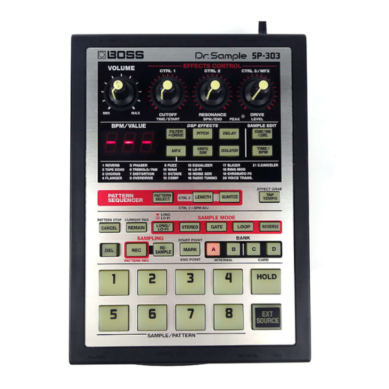
Page 4: Location Of Controls
Mar.2001 SP-303 LOCATION OF CONTROLS fig.panel... -
Page 5: Location Of Controls Parts List
Mar.2001 SP-303 LOCATION OF CONTROLS PARTS LIST Part Code Part Name Description Q'ty 02457512 J R-KNOB SFA BLK/LCG 02451945 9M/M ROTARY POTENTIOMETER RK09L12C 50KAx2(20MM) 13449645 JACK (PIN) YKC21-3049 (4P) RED/WHITE 13429672 MIDI JACK YKF51-5047 02452134 SLIDE SWITCH SLG-12-465A 13449720 DC JACK HEC2305-01-250 02452423 BOTTOM COVER... -
Page 6: Exploded View Parts List
Mar.2001 SP-303 EXPLODED VIEW PARTS LIST EXPLODED VIEW [Parts] fig_exploded.eps Part Code Part Name Description Q'ty 02457512 J R-KNOB SFA BLK/LCG 02451823 PANEL SHEET 02451812 CARD COVER 40347767 LABEL SMARTMEDIA 02236489 FOOT 14.5X14.5 02452423 BOTTOM COVER 40344445 LABEL FCC CAUTION 71785956 PWB ASSY (EXG) - Page 7 Mar.2001 SP-303 fig_exploded.eps...
-
Page 8: Parts List
Mar.2001 SP-303 PARTS LIST fig.part1e SAFETY PRECAUTIONS: SAFETY PRECAUTIONS: The parts marked have safety-related characteristics. Use only listed parts for replacement. The parts marked have PART NUMBER DESCRIPTION MODEL NUMBER safety-related characteristics. Use 22575241 Sharp Key C-20/50 only listed parts for replacement. 2247017300 Knob (orange) DAC-15D... - Page 9 Mar.2001 SP-303 01901989 TC7SET04F(TE85L) IC (CMOS) IC16 on MB 01899167 TC74VHC04FT(EL) IC (CMOS) IC43 on MB 15189210 BA15218F-T2 IC (OP AMP) IC3 on MB 15289105 UPC4570G2-E2 IC (BIPOLAR OP AMP) IC1,IC2,IC4 on MB 15289109 M5216FP-600D IC (BIPOLAR OP AMP) IC5 on MB 15199137 AN7805F IC (V.RGL)
- Page 10 Mar.2001 SP-303 POTENTIOMETER 02451956 RK9K111A 250KRD(25MM) 9M/M ROTARY POTENTIOMETER VR6 on MB 02457556 RK09K113A 50KB(20MM) 9M/M ROTARY POTENTIOMETER VR2,VR3,VR4 on SB 02451945 RK09L12C 50KAx2(20MM) 9M/M ROTARY POTENTIOMETER VR5 on SB CAPACITOR 15359206 ECJ2VF1E104Z 100000 PF/25 V CERAMIC CAPACITOR C148,C149,C150,C240 on SB C60,C61,C62,C63,C65,C66,C67,C68,C69,C70,C73, C77,C92,C97,C99,C101,C102,C106,C107,C109,C115, C116,C118,C121,C122,C123,C133,C134,C140,C141,...
- Page 11 Mar.2001 SP-303 ACCESSORIES (STANDARD) 71785990 OWNER'S MANUAL JAPANESE 71890456 OWNER'S MANUAL ENGLISH 00905756 AC ADAPTOR ACI-100C 00905767 AC ADAPTOR ACI-120C 01018312 AC ADAPTOR ACI-230C 01458278 AC ADAPTOR ACB-230E (230 VE) 12449549 AC ADAPTOR ACB-240(A) 40232389 WARRANTY CARD (JAPAN only) 40451756 LEAFLET ENGLISH/JAPANESE...
-
Page 12: Identifying The Version Number
Mar.2001 SP-303 IDENTIFYING THE VERSION Press the [PATTERN SELECT] button and turn it off if it is lit. When the [PATTERN SELECT] button is lit, pattern save operation is selected NUMBER so be careful. Press either the [C] or [D] button while pressing the [CANCEL] button. Turn on the power of the main unit while pressing the [FILTER+DRIVE], The BANK [C] and [D] buttons light up and the pad corresponding to the [PITCH] and [DELAY] buttons. -
Page 13: How To Update System Software
Mar.2001 SP-303 1. Updating by SmartMedia Insert the SmartMedia that contains the sample data into the SP-303. Turn on the SP-303’s power while pressing the [CANCEL] button. 3 Confirm that the [PATTERN SELECT] button is turned off. What is needed Press the [PATTERN SELECT] button and turn it off if it is lit. -
Page 14: Test Mode & Resorting The Factory Setting
Mar.2001 SP-303 2. Test item list The first number of the 3-digit displayed on the SP-303 and the NUMBER SW which lights up represent the song number being received and the song number already received. The [Test mode] includes the following: Digital circuit test When updating is completed, “End”... - Page 15 Mar.2001 SP-303 5. LINE IN/OUT CHECK Check the function of the CPU (IC23) and FLASH MEMORY 4M, 8M (IC22, IC24). “Lin” appears. Check the function of the CPU RAM (IC23) and DRAM (IC27). Check the function of the signal input to INPUT L and R at the time of output Check the function of the DSP (IC9) and CPU (IC23).
- Page 16 Mar.2001 SP-303 8. CARD CHECK fig.fig1 “Crd” appears. Check the loading and writing function of the SmartMedia. When executing this test, always use the SmartMedia initialized in the [Initializing SmartMedia.] procedure. Insert initialized but not write protected SmartMedia. “Wr” appears and the dot blinks, and writing test is executed automatically. “rd”...
-
Page 17: Error Message
Mar.2001 SP-303 ERROR MESSAGE In usual function, when problems occur is the test mode function, the following letters appear. Err cause: Error in test items other than the device check cause:4M Flash ROM device error (Solder, pattern and device defection, and device mistake of the 4MB FLASH ROM IC) 8M Flash ROM device error (Solder, pattern and device defection, and device mistake of the... -
Page 18: About The Shaping Of The Wiring
Mar.2001 SP-303 ABOUT THE SHAPING OF THE FIG12.eps WIRING After disassembling the SP-303 for replacing the basal board and when hearing a noise in [10. NOISE CHECK] in [Return to test mode & factory shipment condition], always shape the ribbon cable 1-4 (P/No.02671167, 02671178, 02671189, 02671190) as described in the figure below. - Page 19 Mar.2001 SP-303 2. RIBON CABLE 14P (P/ 3. RIBON CABLE 13P (P/ No.02671189) shaping method No.02671178), RIBON CABLE 11P (P/No.02671167) shaping Bend the SW board (P/No. 71785978) and RIBBON CABLE 14P (P/ method No.02671189) vertically, then bend and make a fold line at about 3 cm position from the main board of the RIBBON CABLE 14P (P/No.02671189) fig.ribon21 Same shaping method can be used for these 2 ribbon cables.
-
Page 20: Block Diagram
Mar.2001 SP-303 BLOCK DIAGRAM FIG_BLOCK.eps VR6(MIC VOLUME) MIC IN LINE IN L LINE IN R MIDI IN CODE Photo Coupler (IC35 (IC25) RIBON CABLE 5P VR5(VOLUME) X'tal(X RIBON CABLE 13P LOGIC (IC43) RIBON CABLE 13P Peak LED RIBON CABLE 14P CPU(I (LED34) RIBON CABLE 14P... - Page 21 Mar.2001 SP-303 FIG_BLOCK.eps LINE OUT L LINE OUT R PHONES 4M SRAM MUTE TR (IC13) (Q15~18) DSP(IC9) RESET (IC28) C23) X'tal(X1) 3.3V ➝ 5V GA(IC14) LOGIC (IC16) Memory 4M Flash Memory (IC22) ARRAY Smart Media K DIAGRAM...
-
Page 22: Circuit Board
Mar.2001 SP-303 CIRCUIT BOARD fig_compornent.eps... - Page 23 Mar.2001 SP-303 fig_compornent.eps View from compornent side...
-
Page 24: Circuit Board
Mar.2001 SP-303 CIRCUIT BOARD fig_foil.eps... - Page 25 Mar.2001 SP-303 fig_foil.eps View from foil side...
-
Page 26: Circuit Diagram(Digital1)
Mar.2001 SP-303 CIRCUIT DIAGRAM(DIGITAL1) fig.digital1 D 3. 3 C223 0.01 IC43F SW SCAN TC74VHC04FT D 3. 3 IC43G TO SW BOARD TC74VHC04FT CN10 C249 C250 C251 0.01 0.01 0.01 EXBA10E103J D 3. 3 RIBON CABLE 13P C110 10/16 EXBV8V470JV C111 0.01 C112 0.01... - Page 27 Mar.2001 SP-303 fig.digital1 GA-DMA-REQ0 GA-DMA-REQ0 GA-DMA-REQ1 GA-DMA-REQ1 GA-DMA-ACK0 4M FLASH ROM GA-DMA-ACK0 GA-DMA-ACK1 GA-DMA-ACK1 A-1/DQ15 IC22 DQ14 LH28F400BVE-BL85 DQ13 CPU-RD CPU-RD DQ12 CPU-UCAS CPU-UCAS DQ11 D 3. 3 CPU-LCAS CPU-LCAS DQ10 D 3. 3 N2012Z601T02 CLOCK-OUT CLOCK-OUT R193 DSP-INT DSP-INT RA12 DSP-INT1 EXBA10E103J...
-
Page 28: Circuit Diagram(Digital2)
Mar.2001 SP-303 CIRCUIT DIAGRAM(DIGITAL2) fig.digital2 CONTROL[0-50] DATA[0-15] ADDRESS[0-23] D 3. 3 GA-DMA-REQ0 N2012Z601T0 GA-DMA-REQ0 GA-DMA-REQ1 GA-DMA-REQ1 GA-DMA-ACK0 GA-DMA-ACK0 D 3. 3 GA-DMA-ACK1 GA-DMA-ACK1 R234 CPU-RD CPU-RD CPU-UCAS CPU-UCAS CPU-LCAS CPU-LCAS CLOCK-OUT CD_CLE CLOCK-OUT R233 DSP-INT CD_XCE DSP-INT 1.5K DSP-INT1 CD_ALE DSP-INT1 RESET CD_XRE... - Page 29 Mar.2001 SP-303 fig.digital2 D 3. 3 C287 0.001 Smart Media 10/16 3VSW1 C288 0.001 3VSW2 5VSW1 5VSW2 R245 C104 WPSW2 TC203C040AF-001(MR2) RESET WPSW1 C103 4.7k MA-406 33.8688MHz OSC1 CPU-LCAS I/O1 CPU-RD I/O2 IC13 I/O8 UPD431000AGW-70LL-E2 I/O3 I/O7 I/O4 I/O8 EA11 I/O6 I/O7 I/O6...
-
Page 30: Circuit Diagram(Analog)
Mar.2001 SP-303 CIRCUIT DIAGRAM(ANALOG) fig.analog C152 R123 N2012Z601T02 MIC VOLUME 0.01 C154 R126 VR6A R125 N2012Z601T02 22/16 250kRD LGR4609-7000 R128 C308 C224 R129 0.22/50 1/50 R124 MIC IN MA147-(TX) R207 4.7k C246 N2012Z601T02 C155 R208 C225 IC1B 4.7k 10/16 UPC4570G 4.5v(M) C242 C160... - Page 31 Mar.2001 SP-303 fig.analog IC1C IC4C UPC4570G UPC4570G IC3C IC2C IC5C BA15218F UPC4570G M5216FP A +9V A +9V A+4.5V A+4.5V (MIC (EXCEPT ONLY) R127 4.5v(M) MIC) IC1A UPC4570G R130 C156 10/16 470/6.3 VR5C RK09L1220 50KA N2012Z601T02 VR6B D 3. 3 C211 C161 C305 250kRD...
-
Page 32: Circuit Diagram(Sw)
Mar.2001 SP-303 CIRCUIT DIAGRAM(SW) fig_SW.eps CTRL 3 /MFX CTRL 1 CTRL 2 RK09K 50kB RK09K 50kB RK09K 50kB LED1 LNJ208R8ARA MARK LED3 LNJ208R8ARA STEREO LED5 LNJ208R8ARA IC33 IC34 BU2090F LED7 SML-010LTT86 BU2090F SOURCE LED9 SML-010LTT86 DATA DATA CLOCK CLOCK LED11 SML-010LTT86 LED13 SML-010LTT86... - Page 33 Mar.2001 SP-303 fig_SW.eps LED2 LNJ208R8ARA LENGTH R112 LED26 LNJ208R8ARA REVERSE LED4 LNJ208R8ARA SONG LED28 LNJ208R8ARA R114 LOOP LED30 LNJ208R8ARA R116 IC44 LED8 LNJ208R8ARA BU2090F VINTYL LED32 LNJ208R8ARA R118 LED10 LNJ208R8ARA DATA LED25 LNJ208R8ARA R111 GATE CLOCK LED12 LNJ208R8ARA FILTER+OD R113 LED27 LNJ208R8ARA LED14...
-
Page 34: Circuit Diagram(Power)
Mar.2001 SP-303 CIRCUIT DIAGRAM(POWER) fig.power DIGITAL +3.3V D 3. 3 ELC10D221E 2SA1706S-AN R187 R188 C213 C214 SB07-03N 1.6k(METAL) 1000/6.3 IC30 NJM2360AF R189 R190 1k(METAL) R191 0.33(1/2W) VIN- C216 150p DIGITAL +5V IC31 GA,7SEG LED Tr ARRAY AN7805 DSP,DSP MEMORY C139 C140 C141 1000/6.3... - Page 35 Mar.2001 SP-303...
- Page 36 Mar.2001 SP-303...