Table of Contents
Advertisement
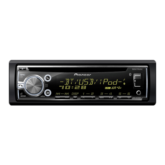
CD RDS RECEIVER
DEH-X6700BS
DEH-X5700BT
DEH-X6710BT
DEH-X6700BT
DEH-X6790BT
DEH-X6750BT
DEH-X6750BT
This service manual should be used together with the following manual(s):
Model No.
Order No.
CRT4759
CX-3287
PIONEER CORPORATION
PIONEER ELECTRONICS (USA) INC. P.O. Box 1760, Long Beach, CA 90801-1760, U.S.A.
PIONEER EUROPE NV Haven 1087, Keetberglaan 1, 9120 Melsele, Belgium
PIONEER ELECTRONICS ASIACENTRE PTE. LTD. 253 Alexandra Road, #04-01, Singapore 159936
PIONEER CORPORATION 2014
Mech. Module
S11.6STD
CD Mech. Module : Circuit Descriptions, Mech. Descriptions, Disassembly
1-1, Shin-ogura, Saiwai-ku, Kawasaki-shi, Kanagawa 212-0031, Japan
DEH-X6700BS/XNUC
/XNEW5
/XNUC
/XNUC
/XNID
/XNGS
/XNCS
Remarks
ORDER NO.
CRT5560
/XNUC
K-ZZZ JUNE 2014 Printed in Japan
Advertisement
Table of Contents

Related Manuals for Pioneer DEH-X6700BS/XNUS


Summary of Contents for Pioneer DEH-X6700BS/XNUS
- Page 1 PIONEER CORPORATION 1-1, Shin-ogura, Saiwai-ku, Kawasaki-shi, Kanagawa 212-0031, Japan PIONEER ELECTRONICS (USA) INC. P.O. Box 1760, Long Beach, CA 90801-1760, U.S.A. PIONEER EUROPE NV Haven 1087, Keetberglaan 1, 9120 Melsele, Belgium PIONEER ELECTRONICS ASIACENTRE PTE. LTD. 253 Alexandra Road, #04-01, Singapore 159936...
-
Page 2: Safety Information
SAFETY INFORMATION CAUTION This service manual is intended for qualified service technicians; it is not meant for the casual do-it-yourselfer. Qualified technicians have the necessary test equipment and tools, and have been trained to properly and safely repair complex products such as those covered by this manual. Improperly performed repairs can adversely affect the safety and reliability of the product and may void the warranty. - Page 3 CAUTION Danger of explosion if battery is incorrectly replaced. Replaced only with the same or equivalent type recommended by the manufacturer. Discord used batteries according to the manufacturer's instructions. DEH-X6700BS/XNUC...
-
Page 4: Table Of Contents
CONTENTS SAFETY INFORMATION............................. 2 1. SERVICE PRECAUTIONS ..........................5 1.1 SERVICE PRECAUTIONS......................... 5 1.2 NOTES ON SOLDERING .......................... 5 2. SPECIFICATIONS ............................6 2.1 SPECIFICATIONS............................6 2.2 DISC/CONTENT FORMAT ........................6 3. BASIC ITEMS FOR SERVICE.......................... 6 3.1 CHECK POINTS AFTER SERVICING....................... 6 3.2 PCB LOCATIONS ............................ -
Page 5: Service Precautions
1. SERVICE PRECAUTIONS 1.1 SERVICE PRECAUTIONS 1. You should conform to the regulations governing the product (safety, radio and noise, and other regulations), and should keep the safety during servicing by following the safety instructions described in this manual. 2. Before disassembling the unit, be sure to turn off the power. Unplugging and plugging the connectors during power-on mode may damage the ICs inside the unit. -
Page 6: Specifications
2.2 DISC/CONTENT FORMAT The Bluetooth word mark and logos are owned by the Bluetooth SIG, Inc. and any use of such marks by Pioneer Corporation is under license. Other trademarks and trade names are those of their respective owners. 3. BASIC ITEMS FOR SERVICE 3.1 CHECK POINTS AFTER SERVICING... -
Page 7: Pcb Locations
3.2 PCB LOCATIONS CD Core Unit (S11.6VA) BT Unit Tuner Amp Unit Keyboard Unit A:DEH-X6700BS/XNUC B:DEH-X5700BT/XNEW5 C:DEH-X6710BT/XNUC D:DEH-X6700BT/XNUC E:DEH-X6790BT/XNID F:DEH-X6750BT/XNGS G:DEH-X6750BT/XNCS Unit Name : Keyboard Unit Unit Name : Tuner Amp Unit Unit Number : (A,C,D,E,F,G) Unit Number : QWM3861(A) Unit Number : (B) Unit Number... -
Page 8: Block Diagram
4. BLOCK DIAGRAM 4.1 BLOCK DIAGRAM RL/SW RR/SW BT MIC Power Connector JA892 WIRED REMOTE, MIC & AUX2 JA401 JA901 CD CORE UNIT Connector flex 7.4V 1. VD Q751 KTD2092(QR) 2. VD B.up CD S11.6 STD 3. /CDSRQ VD SENS IC30 4. - Page 9 A DEH-X6700BS/XNUC B DEH-X5700BT/XNEW5 JA961 Sxi BUS JA251 R/SW CKS3806 P251 YEK5001-A CEK1386 750mA B.up RCA GND P1002 IC301 FSMD07524-R IC POWER AMP B.up PAL013A BREM& A.ANT RCA MUTE STBY MUTE STBY +B 5.75 MUTE SYS+B SYS+B SXML0 SXMR0 SXMG0 Sxi BUFFER SXiTOSYS SXiTx...
- Page 10 RL/SW RR/SW BT MIC Power Connector JA892 WIRED REMOTE JA401 & JA901 CD CORE UNIT Connector flex 1. VD 7.4V Q751 KTD2092(QR) 2. VD B.up 3. /CDSRQ CD S11.6 STD VD SENS VD CONT 4. CDSTBY CDSKIP,CDRST CXK5805 5. SCL CDSRQ,CDSTBY 6.
- Page 11 C DEH-X6710BT/XNUC D DEH-X6700BT/XNUC E DEH-X6790BT/XNID F DEH-X6750BT/XNGS JA251 G DEH-X6750BT/XNCS R/SW P251 YEK5001-A CEK1386 TUNER AMP UNIT RCA GND IC POWER AMP B.up IC301 PAL013A EFG PA2032A STBY MUTE STBY VDD3.3V SYS+B 5.75 MUTE SYS+B SYS+B RCA MUTE IC681 VDD 3.3V B.up S-Quad Flash...
-
Page 12: Power Block Diagram
4.2 POWER BLOCK DIAGRAM A DEH-X6700BS/XNUC B DEH-X5700BT/XNEW5 SYSPW SW5VCNT VDDCNT TYPE PART NO. B.UP 55.00 mA 38.00 mA PM9013A IC REGURATER SYS+B E-Volume (Analog) IC911 5.60 6.20 Voltage BA49183-V12 Power Amp (standby) (YEK5001-A) Current 60.00 mA 18.00 mA Power Amp (Mute) 216.00 mA Lithio SW 5V... - Page 13 C DEH-X6710BT/XNUC D DEH-X6700BT/XNUC E DEH-X6790BT/XNID F DEH-X6750BT/XNGS G DEH-X6750BT/XNCS SYSPW SW5VCNT VDDCNT TYPE PART NO. B.UP 55.00 mA 38.00 mA PM9013A IC REGURATER SYS+B E-Volume (Analog) IC911 5.60 6.20 Voltage BA49183-V12 10 mA B.REM A.ANT (YEK5001-A) Current 60.00 mA 18.00 mA Power Amp (Mute) 216.00 mA...
-
Page 14: Diagnosis
5. DIAGNOSIS 5.1 OPERATIONAL FLOWCHART Power ON (DEH-X6700BS/XNUC, DEH-X5700BT/XNEW5) Vcc : Pin 15, 26, 51, 93, 104, 130 Vcc = 1.2 V PVcc = 3.3 V PVcc : Pin 3, 11, 22, 34, 44, 58, 81, 89, 100, 119, 126, 136 BSENS Pin 108 BSENS = L... - Page 15 Power ON (DEH-X6710BT/XNUC, DEH-X6700BT/XNUC, DEH-X6790BT/XNID, DEH-X6750BT/XNGS, DEH-X6750BT/XNCS) Vcc : Pin 12, 20, 43, 78, 86, 109 Vcc = 1.2 V PVcc = 3.3 V PVcc : Pin 3, 16, 28, 36, 48, 69, 82,101, 112 BSENS Pin 90 BSENS = L ASENS Pin 89 ASENS = L...
-
Page 16: Error Code List
5.2 ERROR CODE LIST ERROR CODES If a CD memory device is inoperable, or operation of such media is stopped by an error, the error mode is established and a cause of the error is displayed by an error code. Indication of error codes is intended to reduce the number of calls from customers and facilitate failure analysis and repair work in servicing. - Page 17 Symptoms are written in bold and causes in reg- USB storage device/iPod ular, non-indented text. Regular, indented text is FORMAT READ used to indicate actions to be taken. Sometimes there is a delay between the start of play- back and when you start to hear any sound. Common Wait until the message disappears and you hear sound.
- Page 18 NO BT DEVICE GO TO BT MENU TO REGISTER If the error message is still displayed after performing the above action, please contact your No Bluetooth device found. dealer or an authorized Pioneer Service Station. Follow the instructions that appear on the screen. Pandora CONN.
- Page 19 If the message fails to disappear even after the engine is switched off/on, contact your dealer or NO NETWORK an authorized Pioneer Service Station for The connected device is out of area. assistance. Connect the connected device to a network.
-
Page 20: Connector Function Description
5.3 CONNECTOR FUNCTION DESCRIPTION REAR OUTPUT DEH-X6700BS/XNUC Sirius XM BUS FM/AM ANTENNA INPUT MICROPHONE WIRED FRONT INPUT REMOTE OUTPUT 15 13 11 9 7 5 3 1 CONTROL Sirius XM BUS 16 14 12 10 8 6 4 2 SUBWOOFER OUTPUT 1 FL+ 9 NC 10 NC... -
Page 21: Service Mode
6. SERVICE MODE 6.1 DISPLAY TEST MODE 1 [How to enter Test mode] Press and hold "PHONE" and "LIST" buttons together, and turn BUP and ACC on. SOURCE LIST PHONE BAND BACK Grille condition Conf. item Operate Show LCD All light up PHONE + LIST Draw 1 White... -
Page 22: Display Test Mode 2
6.2 DISPLAY TEST MODE 2 The information such as the system microcomputer version is checked. [How to enter Test mode] Press and hold "1" and "3" buttons together, and turn BUP and ACC on. [Operation key] Operation key Processing Remarks Enter display test mode 1 + 3 Switch to next test mode... -
Page 23: Software Version Up Method
6.3 SOFTWARE VERSION UP METHOD Overview This mode is used for upgrading the MCU software of system using USB memory. How to enter in USB rewriting mode Press and hold "1" and "2" buttons together, and turn BUP and ACC on. USB rewriting operation flow Explanatory note Screen display and ON/OFF of illumination... -
Page 24: Cd Test Mode
6.4 CD TEST MODE - Flow Chart To enter the test mode: [4] + [6] -> BUP + ACC ON [Key] [CD] or [SOURCE] Source ON Contents Display [BAND] Power On RF AMP (T.Offset is adjusted) Gain switching 00 00 00 [BAND] [>] [<]... -
Page 25: Disassembly
7. DISASSEMBLY While the photograph shown is slightly different from this model in shape, the disassembly procedure is the same. - Removing the Panel Assy (Fig.1) Release the two latches. Release the two latches and then remove the Panel Assy. Panel Assy Fig.1 - Removing the CD Mechanism Module (Fig.2) - Page 26 - Removing the Tuner Amp Unit and the BT Unit (Fig.3) Tuner Amp Unit Disconnect the connector. Remove the two screws. Remove the screw. (X6700BS/XNUC,X5700BT/XNEW5) Remove the two screws and then remove the Tuner Amp Unit. Remove the screw and then remove the BT Unit.
- Page 27 Disassembling the Panel Part (Fig.5, 6) 1. Remove the arm while bending the rib of the panel upward. Fig.5 2. Press the upside hook and the bottom side hook of the button at the same time, and pull out the button. Fig.6 Assembling the Panel Part (Fig.7, 8, 9) 1.
- Page 28 3. Fit the spring in the groove at the position shown in the figure. 4. Fit the boss on the lower side of the arm in the lower hole of the panel, and then warp the rib on the panel in the direction shown in the figure and fit the boss of the arm in the panel.
- Page 29 How to carry the mecha unit 1. Hold the designated points (shown with dashed lines) of the upper chassis and the front/rear bracket. 2. Be careful not to hold the solid line portions or the CRG mecha part or insert foreign substances, to prevent distortion. 3.
- Page 30 How to remove the PU unit 1. Create an empty-clamp state according to “How to create empty clamp state (motor drive)”. 2. Hook the feeding screw biasing spring to a tentative hooking portion (Fig 2b). Be careful not to get injured by the spring edge.
-
Page 31: Each Setting And Adjustment
8. EACH SETTING AND ADJUSTMENT 8.1 CD ADJUSTMENT 1) Cautions on adjustments 2) Test mode This mode is used to adjust the CD mechanism module. In this product the single voltage (3.3 V) is used for the regulator. The reference voltage is the REFO1 (1.65 V) To enter the test mode. -
Page 32: Checking The Grating After Changing The Pickup Unit
8.2 CHECKING THE GRATING AFTER CHANGING THE PICKUP UNIT Note : The grating angle of the PU unit cannot be adjusted after the PU unit is changed. The PU unit in the CD mechanism module is adjusted on the production line to match the CD mechanism module and is thus the best adjusted PU unit for the CD mechanism module. - Page 33 Grating waveform Ech -> Xch 20 mV/div, AC Fch -> Ych 20 mV/div, AC 0 degrees 30 degrees 45 degrees 60 degrees 75 degrees 90 degrees DEH-X6700BS/XNUC...
-
Page 34: Pcl Output Confirmation
8.3 PCL OUTPUT CONFIRMATION (DEH-X6700BS/XNUC, DEH-X5700BT/XNEW5) - PCL Output In the normal operation mode (with the detachable panel installed, the ACC switched ON, the standby mode cancelled), shift the TESTIN IC601(Pin 117) terminal to H. The clock signal is output from the PCL_RAM_MON terminal IC601(Pin140). The frequency of the clock signal is 600 kHz that is divided by 20th of the oscillation frequency of X601 (12MHz). - Page 35 DEH-X6700BS/XNUC...
-
Page 36: Exploded Views And Parts List
9. EXPLODED VIEWS AND PARTS LIST OTES : Parts marked by " * " are generally unavailable because they are not in our Master Spare Parts List. The > mark found on some component parts indicates the importance of the safety factor of the part. Therefore, when replacing, be sure to use parts of identical designation. - Page 37 (1) PACKING SECTION PARTS LIST Mark No. Description Part No. Mark No. Description Part No. 12-4 Caution Card See Contrast table (2) Protector See Contrast table (2) Microphone Assy CPM1083 12-5 Caution Card See Contrast table (2) Holder CZN7192 12-6 Warranty Card See Contrast table (2) Cushion CZN7193...
- Page 38 * QRB3460 Finnish * QRB3461 Danish * QRB3462 Portuguese * QRB3463 Greek * QRB3464 Turkish All operation manuals are supplied in PDF files by the CD-ROM. Regarding the availability of paper manual, contact Pioneer Service representative in your region. DEH-X6700BS/XNUC...
- Page 39 DEH-X6700BS/XNUC...
-
Page 40: Exterior
9.2 EXTERIOR X6700BS/XNUC X6710BT/XNUC X6700BT/XNUC X6790BT/XNID X6750BT/XNGS X6750BT/XNCS X6700BS/XNUC X6710BT/XNUC X6700BT/XNUC X6700BS/XNUC X6790BT/XNID X6750BT/XNGS X5700BT/XNEW5 X6750BT/XNCS X6710BT/XNUC X6700BT/XNUC X6790BT/XNID X6750BT/XNGS X6750BT/XNCS X5700BT/XNEW5 DEH-X6700BS/XNUC... - Page 41 (1) EXTERIOR SECTION PARTS LIST Mark No. Description Part No. Mark No. Description Part No. QNV3025 Screw ASZ26P050FTC Button QNV3026 Screw BSZ26P060FTC Detachable Grille Assy See Contrast table (2) Screw BSZ26P080FTC Screw BPZ20P100FTC Screw BSZ26P120FTC Spring CBH2210 CD Mechanism Module (S11.6VA) CXK5805 Button (EJECT) QAC3166...
- Page 42 DEH-X6750BT/ DEH-X6750BT/ Mark Description XNGS XNCS Heat Sink QNR3002 QNR3010 Detachable Grille QXA4157 QXA4156 Assy Knob Unit QXA3694 CXE3692 Grille Unit QXA4130 QXA4129 Card Remote QXE1044 QXE1044 Control Unit Cover CNS7068 CNS7068 Sheet Not used Not used DEH-X6700BS/XNUC...
- Page 43 DEH-X6700BS/XNUC...
-
Page 44: Cd Mechanism Module
9.3 CD MECHANISM MODULE (A) : GEM1024 (B) : GEM1043 DEH-X6700BS/XNUC... - Page 45 CD MECHANISM MODULE SECTION PARTS LIST Mark No. Description Part No. Mark No. Description Part No. Damper CNW1198 ..Screw BSZ20P040FTC CNW1726 Screw(M2 x 4) CBA1835 Motor Unit(M2)(LOAD/CRG) CXC4026 Washer CBF1038 Screw Unit CXC8894 Spring CBH3010 Arm Assy CXE6232 Washer CBF1037 Spring CBH2855...
-
Page 46: Schematic Diagram
10. SCHEMATIC DIAGRAM 10.1 TUNER AMP UNIT (DEH-X6700BS, DEH-X5700BT) (1/2 scale) Note: When ordering service parts, be sure to refer to " EXPLODED VIEWS AND PARTS LIST" or "ELECTRICAL PARTS LIST". CN701 FM/AM ANTENNA R454 C454 TUNER C707 CN701 JA401 C708 FM(30%): -18.0 dBs VKN1192-... - Page 47 MODEL C707 TUNER AMP UNIT DEH-X6700BS/XNUC C708 C233 C202 DEH-X5700BT/XNEW5 1u/10 R720 C242 C236 1u/10 C204 1u/10 C206 1u/10 C221 C239 FM: -6.0 dBs FM: -2.0 dBs C710 1u/10 AM: -6.0 dBs AM: -2.0 dBs AUX:+10.2 dBs AUX:+10.2 dBs C241 CD:+10.2 dBs CD:+10.2 dBs 1000p/50...
-
Page 48: Tuner Amp Unit (Except Deh-X6700Bs, Deh-X5700Bt) (1/2 Scale)
10.2 TUNER AMP UNIT (Except DEH-X6700BS, DEH-X5700BT) (1/2 scale) CN701 TUNER FM/AM ANTENNA FM(30%):-18.0 dBs C707 NM AM(30%):-18.0 dBs CN701 JA401 TP412 C708 VKN1192- C406 TUNL YKS5041- TUNGND C402 TUNR R720 L407 KN401 M2R6TP_GND R451 C710 Ref. C,D,G 0.1u/16 R701 R409 R411 L406... - Page 49 TUNER AMP UNIT C707 NM C708 C233 C202 1u/10 C236 MODEL R720 1u/10 C DEH-X6710BT/XNUC C204 1u/10 C710 D DEH-X6700BT/XNUC C206 1u/10 0.1u/16 C221 REFERENCE AREA MAP C237 1000p/50 EVOL 201 - 250 MECHA VD 751 - 800 E DEH-X6790BT/XNID 1u/10 251 - 300 GRILL...
-
Page 50: Keyboard Unit
10.3 KEYBOARD UNIT KEY MATRIX GRILLE uCON C1801 CCG1212-A S1821 S1822 S1823 S1824 X1801 CSS1547- CSG1155- CSG1155- CSG1155- CSG1155- DGND EJECT RIGHT BAND LEFT KST0 DGND SEG15 DPDT S1825 S1826 S1827 SEG16 KYDT SEG17 URX/P35 SEG18 R1802 FT8C UTX/P34 CSG1155- CSG1155- CSG1155- BACK... - Page 51 DEH-X6700BS/XNUC KEYBOARD UNIT DEH-X5700BT/XNEW5 DEH-X6710BT/XNUC DEH-X6700BT/XNUC DEH-X6790BT/XNID DEH-X6750BT/XNGS S1824 DEH-X6750BT/XNCS CSG1155- BAND S1827 CSG1155- BACK KYDT DPDT S1831 SOURCE CONNECTOR CSG1155- CN1941 CKS6451 DGND ILMGND DGND SWVDD L1941 ILMGND SWVDD MULTI-CONTROL ROT1 ILM+B S1836 ILM+B KDT2 ROT0 USBGND R1941 1/10W KST1 KYDT 2.2k...
-
Page 52: Cd Core Unit (S11.6Va)
10.4 CD CORE UNIT (S11.6VA) PU UNIT(P11)(SERVICE) CXX4754 V3R3 PUEN Q102 Vref LTA123JUB R111 R110 LD_CURRENT Q101 R109 1.5k 2SA1577(QR) ATEST VREF A.Vdd1 C221 V+3A A.GND1 0.1u/10 C216 1500p/50 AGCO RFAGC C220 HOLOGRAM UNIT C219 0.1u/10 AGCI 0.1u/10 FOCUS ACT C228 R229 TRK ACT... - Page 53 CD CORE UNIT(S11.6VA) C302 C303 1000p/50 1000p/50 PUEN C304 0.022u/16 C305 0.1u/10 R310 4.7k R311 4.7k R312 4.7k R313 4.7k TEMP TEMP R215 TH201 TESTIN ATEST BSCK0 /WAIT A.Vdd1 A.GND1 C216 R291 1500p/50 LRCK AGCO /WAIT C283 TX/EMPH C219 BCLK AGCI LRCK C281...
-
Page 54: Bt Unit
10.5 BT UNIT BT MODULE 1u/10 CN21 CKS6346- MIC_BIAS BT18ON MIC1P BT1.8V MIC1N BOOTS 3.3V BT1.8V RESET BT1.8V BT3.3V IC21 DBG_Tx DBG_Rx VOUT MM3479A18P DEH-X6700BS/XNUC... - Page 55 BT UNIT CN23 CKS3857-A 1u/10 BTDATA BTSCK BTRLCK CN971 NRST_CPU 3.3V SYSTOBT BTTOSYS IC22 BT3.3V VOUT MIC1P MIC1N MM3411A33N DEH-X6700BS/XNUC...
-
Page 56: Waveforms
10.6 WAVEFORMS - CD CORE UNIT(S11.6VA) Note : 1. The encircled numbers denote measuring points in the circuit diagram. 2. Reference voltage REFO1(1.65 V) 1DSCSNS 1DSCSNS 5 V/div 500 ms/div 5 V/div 500 ms/div 3HOME 5CLCONT 5 V/div 5 V/div 4LOEJ 4LOEJ 5 V/div... - Page 57 fRFAGC fRFAGC gLRCK 1 V/div 2 ms/div 1 V/div 200 ms/div 2 V/div 10 us/div hBCLK 500 mV/div 1 V/div 2 V/div 9TIN 8CIN 500 mV/div 500 mV/div DOUT(DATA) 2 V/div 7SIN 2 V/div 32 Tracks Jump waveform Search operation(Outter to Inner) Digital Out waveform (Zoom of 100 Track Jump waveform) Ref.:...
-
Page 58: Pcb Connection Diagram
11. PCB CONNECTION DIAGRAM 11.1 TUNER AMP UNIT (DEH-X6700BS, DEH-X5700BT) NOTE FOR PCB DIAGRAMS TUNER AMP UNIT 1.The parts mounted on this PCB include all necessary parts for several destination. For further information for respective destinations, be sure W.REM to check with the schematic dia- JA891 gram. - Page 59 SIDE A FM/AM ANTENNA JA961 POWER SUPPLY C326 L901 JA901 IC301 VA965 VA963 VA961 C325 VA962 VA964 R961 C963 R962 R966 R965 C333 C334 C332 VA966 R964 C335 C961 C305 C324 C323 D902 D901 C313 D302 R963 C965 C969 C321 C307 C303 R1013...
- Page 60 TUNER AMP UNIT TESTIN PCL_RAM_MON DEH-X6700BS/XNUC...
- Page 61 SIDE B DEH-X6700BS/XNUC...
-
Page 62: Tuner Amp Unit (Except Deh-X6700Bs, Deh-X5700Bt)
11.2 TUNER AMP UNIT (Except DEH-X6700BS, DEH-X5700BT) TUNER AMP UNIT JA891 W.REM&MIC PREOUT JA892 JA251 C892 C891 C260 R899 R900 R891 VA891 R892 C319 C894 C320 C261 C893 P252 Q252 R893 C331 C333 C33 C317 Q251 VA892 P251 R255 C255 C318 C257 C305... - Page 63 SIDE A FM/AM ANTENNA C326 IC301 POWER SUPPLY L901 Q751 JA901 C752 D751 R752 C320 C325 C331 C333 C334 C332 Q752 C753 C318 C313 C751 C327 C303 C335 C305 C324 D902 R312 R310 C323 D901 C321 C301 C311 R307 C310 D301 C901 C307...
- Page 64 TUNER AMP UNIT TESTIN PCL_RAM_MON DEH-X6700BS/XNUC...
- Page 65 SIDE B AM_MON DEH-X6700BS/XNUC...
-
Page 66: Keyboard Unit
11.3 KEYBOARD UNIT KEYBOARD UNIT S1822 EJECT S1835 S1826 SOURCE LIST S1825 D1845 D1842 PHONE S1836 MULTI-CONTROL D1841 S1827 BAND S1824 LEFT RIGHT DISP BACK S1823 S1828 S1821 S1834 KEYBOARD UNIT R1860 R1856 R1862 R1941 R1942 R1852 R1861 Q1845 R1851 Q1844 R1855 Q1842... - Page 67 SIDE A IC1951 JA1901 V1801 D1843 D1844 JA1921 S1834 S1832 S1833 S1830 S1831 S1829 SIDE B CN801 L1922 C1922 R1922 R1941 L1923 R1923 C1921 CN1941 R1921 L1921 R1802 C1902 L1941 C1851 D1902 C1944 IC1801 L1901 C1903 R1865 Q1847 R1953 R1875 Q1848 C1951 R1876...
-
Page 68: Cd Core Unit (S11.6Va)
11.4 CD CORE UNIT (S11.6VA) CD CORE UNIT(S11.6VA) SIDE A PU UNIT(P11) (SERVICE) TH201 R254 C235 CN101 LOAD/CRG R246 MOTOR R232 HOME S901 C201 CN702 R253 R245 C238 C710 C299 R706 R297 C205 C705 C707 C220 R702 R701 SPDL MOTOR CN701 CN701 C702... - Page 69 CD CORE UNIT(S11.6VA) SIDE B C202 R108 Q102 Q101 C104 X201 R109 R294 C203 C209 C233 C101 R237 C224 C210 C223 C211 R110 R111 R240 R282 C204 C284 R281 C222 IC201 C281 C218 C301 C282 R216 R218 R291 C219 R229 C217 C283 C216...
-
Page 70: Bt Unit
11.5 BT UNIT BT UNIT SIDE A CN971 CN23 BT MODULE CN21 BT UNIT SIDE B DEH-X6700BS/XNUC... -
Page 71: Electrical Parts List
12. ELECTRICAL PARTS LIST NOTE: Parts whose parts numbers are omitted are subject to being not supplied. The part numbers shown below indicate chip components. Chip Resistor RS1/_S___J,RS1/__S___J Chip Capacitor (except for CQS..) CKS.., CCS.., CSZS..The > mark found on some component parts indicates the importance of the safety factor of the part. Therefore, when replacing, be sure to use parts of identical designation. - Page 72 Circuit Symbol and No. Part No. Circuit Symbol and No. Part No. D 805 (A,121,13) Diode DZ2S068C R 402 (A,150,94) RS1/16SS0R0J D 806 (A,117,13) Diode DZ2S068C R 403 (A,140,94) RS1/16SS391J D 807 (A,114,13) Diode DZ2S068C R 404 (A,151,109) RS1/16SS105J D 901 (A,138,127) Diode D1F60-5053 R 405...
- Page 73 Circuit Symbol and No. Part No. Circuit Symbol and No. Part No. R 650 (A,94,74) RS1/16SS102J R 913 (A,154,42) RS1/16SS223J R 651 (A,91,72) RS1/16SS473J R 914 (A,133,41) RS1/16SS223J R 652 (A,95,68) RS1/16SS222J R 930 (A,138,122) RS1/10SR0R0J R 653 (A,97,65) RS1/16SS103J R 941 (A,126,110) RS1/16SS223J...
- Page 74 Circuit Symbol and No. Part No. Circuit Symbol and No. Part No. C 257 (A,30,129) (A) CCSSCH101J50 C 612 (A,125,81) CKSSYB104K10 C 258 (A,25,130) (A) CCSSCH101J50 C 613 (A,124,84) CKSSYB104K10 C 260 (A,34,131) CKSSYB103K16 C 618 (A,126,89) CCSSCH120J50 C 261 (A,6,132) CKSSYB104K10 C 619...
- Page 75 Circuit Symbol and No. Part No. Circuit Symbol and No. Part No. D 941 (A,92,124) Diode DZ2J068M0 C 941 (A,132,112) CKSRYB104K16 D 1011 (A,126,107) Diode CRG03 C 961 (A,149,130) CKSRYB105K16 L 202 (A,93,101) Inductor CTF1793 C 963 (A,137,134) (B) CKSRYB104K16 L 402 (A,137,91) Inductor(C,D,G) LCTAW150J2520...
- Page 76 Circuit Symbol and No. Part No. Circuit Symbol and No. Part No. R 532 (A,90,86) RS1/16SS222J R 668 (A,101,58) RS1/16SS473J R 533 (A,91,86) RS1/16SS222J R 671 (A,128,68) RS1/16SS104J R 681 (A,107,96) RS1/16SS473J R 534 (A,93,86) RS1/16SS272J R 682 (A,109,90) RS1/16SS473J R 535 (A,94,86) RS1/16SS472J...
- Page 77 Circuit Symbol and No. Part No. Circuit Symbol and No. Part No. R 976 (A,96,51) RS1/16SS101J C 418 (A,139,102) (E,F) CCSSCK2R0C50 R 977 (A,90,73) RS1/16SS0R0J C 419 (A,139,103) (E,F) CCSSCK1R0C50 R 978 (A,88,69) RS1/16SS0R0J R 1011 (A,130,107) RS1/16SS103J C 420 (A,145,107) CCSSCH471J50 R 1013...
- Page 78 Circuit Symbol and No. Part No. Circuit Symbol and No. Part No. C 683 (A,119,93) CCSSCJ3R0C50 D 1843 (A,160,23) LED SMLVN6RGB2UK(B) C 685 (A,118,98) (E,F) CKSRYB105K10 D 1844 (A,145,20) LED SMLVN6RGB2UK(B) C 687 (A,121,96) CKSRYB105K10 D 1845 (A,45,20) LED SMLVN6RGB2UK(B) C 701 (A,110,39) CKSSYB103K16...
- Page 79 Circuit Symbol and No. Part No. Circuit Symbol and No. Part No. C 1802 (B,70,21) CKSSYB104K10 R 311 (B,31,10) RS1/16SS472J C 1803 (B,75,9) CKSSYB104K10 R 312 (B,31,11) RS1/16SS472J C 1804 (B,76,9) CKSSYB104K10 R 313 (B,31,12) RS1/16SS472J C 1805 (B,77,9) CKSSYB104K10 R 701 (A,22,38) RS1/16SS101J...
- Page 80 Circuit Symbol and No. Part No. R 28 (A,42,30) RS1/16SS222J R 29 (A,29,40) RS1/16SS102J R 30 (A,29,37) RS1/16SS102J R 38 (A,42,16) RS1/16SS0R0J R 39 (A,41,22) RS1/16SS221J R 40 (A,39,22) RS1/16SS221J R 41 (A,38,22) RS1/16SS221J CAPACITORS C 23 (A,24,39) XCEVW221M4 C 24 (A,6,43) CKSRYB105K10 C 26...