Technics SA-DA10 Service Manual
Av control stereo receiver
Hide thumbs
Also See for SA-DA10:
- Operating instructions manual (96 pages) ,
- Operating instrutions (59 pages) ,
- Operating instructions manual (52 pages)
Table of Contents
Advertisement
file:///C|/Documents%20and%20Settings/Administrateur/Mes%20documents/service/SA-DA10/p01.htm
Service Manual
TOP NEXT
Order No. MD0006112C1
A2
AV Control Stereo Receiver
SA-DA10
Color
(K) ... Black Type
(N) ... Gold Type
PP ... U.S.A. and Canada
FM Tuner Section
Frequency range
Sensitivity
50 dB quieting sensitivity
MONO
STEREO
Total harmonic distortion
MONO
STEREO
S/N
file:///C|/Documents%20and%20Settings/Administrateur/Mes%20documents/service/SA-DA10/p01.htm (1 of 3) [21/01/2007 13:46:55]
87.9-107.9 MHz
11.2 dBf (2•V, IHF'58)
18.3 dBf (4.5•V, IHF'58)
38.3 dBf (45•V, IHF'58)
0.2%
0.3%
Advertisement
Table of Contents

Related Manuals for Technics SA-DA10


Summary of Contents for Technics SA-DA10
-
Page 1: Service Manual
PP ... U.S.A. and Canada FM Tuner Section Frequency range 87.9-107.9 MHz Sensitivity 11.2 dBf (2•V, IHF’58) 50 dB quieting sensitivity MONO 18.3 dBf (4.5•V, IHF’58) STEREO 38.3 dBf (45•V, IHF’58) Total harmonic distortion MONO 0.2% STEREO 0.3% file:///C|/Documents%20and%20Settings/Administrateur/Mes%20documents/service/SA-DA10/p01.htm (1 of 3) [21/01/2007 13:46:55]... - Page 2 2 x 100 W (6Ω) Low frequency damping factor 30 (6Ω) Load impedance Front A or B 4 - 8Ω A and B 8Ω BI-WIRE 6 - 8Ω Center 6 - 8Ω Surround 6 - 8Ω file:///C|/Documents%20and%20Settings/Administrateur/Mes%20documents/service/SA-DA10/p01.htm (2 of 3) [21/01/2007 13:46:55]...
- Page 3 ** Manufactured under license from Digital Theater System.“DTS” and“DTS Digital Surround” are trademarks of Digital Theater Syatem. © 2000 Matsushita Electronics (S) Pte. Ltd. All rights reserved. Unauthorized copying and distribution is a violation of law. •@ TOP NEXT file:///C|/Documents%20and%20Settings/Administrateur/Mes%20documents/service/SA-DA10/p01.htm (3 of 3) [21/01/2007 13:46:55]...
-
Page 4: Table Of Contents
6.2.1 Replacement of the Power IC and Regulator Transistor 6.2.2 Installation of the bottom cover after replacement 7 Type Illustrations of ICs, Transistors& Diodes 8 Terminal Functions of ICs 9 Block Diagram 10 Schematic Diagram 11 Printed Circuit Board file:///C|/Documents%20and%20Settings/Administrateur/Mes%20documents/service/SA-DA10/p02.htm (1 of 2) [21/01/2007 13:47:30]... - Page 5 12 Wiring Connection Diagram 13 Parts Location and Replacement Parts List 13.1 Cabinet 13.1.1 Cabinet Parts Location 13.1.2 Cabinet Parts List 13.2 Electrical Parts List 13.3 Packing Materials& Accessories Parts List 13.4 Packaging file:///C|/Documents%20and%20Settings/Administrateur/Mes%20documents/service/SA-DA10/p02.htm (2 of 2) [21/01/2007 13:47:30]...
-
Page 6: Safety Precaution
*Note: Some exposed parts may be isolated from the chassis by design. These will read infinity. 4. If the measurement is outside the specified limits, there is a possibility of a shock hazard. The equipment should be repaired and rechecked before it is returned to the customer. file:///C|/Documents%20and%20Settings/Administrateur/Mes%20documents/service/SA-DA10/p03.htm (1 of 2) [21/01/2007 13:47:05]... - Page 7 •@ TOP PREVIOUS NEXT file:///C|/Documents%20and%20Settings/Administrateur/Mes%20documents/service/SA-DA10/p03.htm (2 of 2) [21/01/2007 13:47:05]...
-
Page 8: Before Repair And Adjustment
After repairs are completed, restore power gradually using a variac, to avoid over current. Current consumption at AC 120 V, 60 Hz in NO SIGNAL mode should be 750~1050 mA. •@ TOP PREVIOUS NEXT file:///C|/Documents%20and%20Settings/Administrateur/Mes%20documents/service/SA-DA10/p04.htm [21/01/2007 13:47:05]... -
Page 9: Protection Circuitry
2. Determine the cause of the problem and correct it. 3. Turn on the power once again after one minute. Note: When the protection circuitry functions, the unit will not operate unless the power is first turned off and then on again. •@ TOP PREVIOUS NEXT file:///C|/Documents%20and%20Settings/Administrateur/Mes%20documents/service/SA-DA10/p05.htm [21/01/2007 13:47:06]... -
Page 10: Accessories
4 Accessories TOP PREVIOUS NEXT AC power supply cord... 1 pc. AM Loop Antenna Set/... 1 set. FM Indoor Antenna... 1 pc. file:///C|/Documents%20and%20Settings/Administrateur/Mes%20documents/service/SA-DA10/p06.htm (1 of 2) [21/01/2007 13:47:06]... - Page 11 Remote Control/Transmitter... 1 pc. •@ TOP PREVIOUS NEXT file:///C|/Documents%20and%20Settings/Administrateur/Mes%20documents/service/SA-DA10/p06.htm (2 of 2) [21/01/2007 13:47:06]...
-
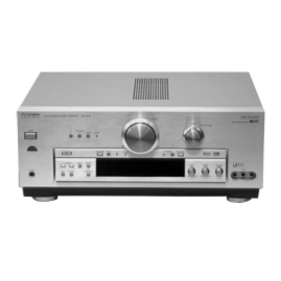
Page 12: Front Panel Controls
5 Front Panel Controls TOP PREVIOUS NEXT 5.1 Front Panel 5.2 Remote Control •@ TOP PREVIOUS NEXT file:///C|/Documents%20and%20Settings/Administrateur/Mes%20documents/service/SA-DA10/p07.htm [21/01/2007 13:47:06]... -
Page 13: Front Panel
5.1 Front Panel TOP PREVIOUS NEXT file:///C|/Documents%20and%20Settings/Administrateur/Mes%20documents/service/SA-DA10/p08.htm (1 of 2) [21/01/2007 13:47:07]... - Page 14 •@ TOP PREVIOUS NEXT file:///C|/Documents%20and%20Settings/Administrateur/Mes%20documents/service/SA-DA10/p08.htm (2 of 2) [21/01/2007 13:47:07]...
-
Page 15: Remote Control
5.2 Remote Control TOP PREVIOUS NEXT •@ TOP PREVIOUS NEXT file:///C|/Documents%20and%20Settings/Administrateur/Mes%20documents/service/SA-DA10/p09.htm [21/01/2007 13:47:07]... -
Page 16: Operation Checks And Main Component Replacement Procedures
2. Installation of the bottom cover after replacement....................... P.g. 15 6.1 Checking Procedure for each major P.C.B. 6.2 Main Component Replacement Procedures 6.2.1 Replacement of the Power IC and Regulator Transistor 6.2.2 Installation of the bottom cover after replacement file:///C|/Documents%20and%20Settings/Administrateur/Mes%20documents/service/SA-DA10/p10.htm (1 of 2) [21/01/2007 13:47:07]... - Page 17 •@ TOP PREVIOUS NEXT file:///C|/Documents%20and%20Settings/Administrateur/Mes%20documents/service/SA-DA10/p10.htm (2 of 2) [21/01/2007 13:47:07]...
- Page 18 6.1 Checking Procedure for each major P.C.B. TOP PREVIOUS NEXT Step 1& Step 2 Unscrew and remove top cabinet as shown. file:///C|/Documents%20and%20Settings/Administrateur/Mes%20documents/service/SA-DA10/p11.htm (1 of 17) [21/01/2007 13:47:10]...
- Page 19 Step 3 Remove all the screws. file:///C|/Documents%20and%20Settings/Administrateur/Mes%20documents/service/SA-DA10/p11.htm (2 of 17) [21/01/2007 13:47:10]...
- Page 20 Step 4 Remove all the screws. Step 5 Remove the two support bars and VGCA cover. file:///C|/Documents%20and%20Settings/Administrateur/Mes%20documents/service/SA-DA10/p11.htm (3 of 17) [21/01/2007 13:47:10]...
- Page 21 Step 6 Release the connectors CP451 and CP506. Step 7 Remove the screw. file:///C|/Documents%20and%20Settings/Administrateur/Mes%20documents/service/SA-DA10/p11.htm (4 of 17) [21/01/2007 13:47:10]...
- Page 22 Step 8 Release the connectors CN351 and CP353. file:///C|/Documents%20and%20Settings/Administrateur/Mes%20documents/service/SA-DA10/p11.htm (5 of 17) [21/01/2007 13:47:10]...
- Page 23 Step 9 Release the flat cable from CN901B./Take note of CN504, CN505 and CN902. file:///C|/Documents%20and%20Settings/Administrateur/Mes%20documents/service/SA-DA10/p11.htm (6 of 17) [21/01/2007 13:47:10]...
- Page 24 Step 10 Remove all the screws and support bar (A). Step 11 Unscrew the nut from AL Panel and remove the Volume Knob. file:///C|/Documents%20and%20Settings/Administrateur/Mes%20documents/service/SA-DA10/p11.htm (7 of 17) [21/01/2007 13:47:10]...
- Page 25 Step 12 Remove all the screws and pull the Volume P.C.B. up as shown./Take note of CP501 and CP502. file:///C|/Documents%20and%20Settings/Administrateur/Mes%20documents/service/SA-DA10/p11.htm (8 of 17) [21/01/2007 13:47:10]...
- Page 26 Step 13 Lift up Panel P.C.B. and remove all connectors. file:///C|/Documents%20and%20Settings/Administrateur/Mes%20documents/service/SA-DA10/p11.htm (9 of 17) [21/01/2007 13:47:10]...
- Page 27 Step 14 Remove all the screws. Step 15 Remove Selector Knobs, Tone Knob, Selector Ring, Light Guide and unscrew the nut./Take note of CP503. file:///C|/Documents%20and%20Settings/Administrateur/Mes%20documents/service/SA-DA10/p11.htm (10 of 17) [21/01/2007 13:47:10]...
- Page 28 Step 16 Remove all the screws. file:///C|/Documents%20and%20Settings/Administrateur/Mes%20documents/service/SA-DA10/p11.htm (11 of 17) [21/01/2007 13:47:10]...
- Page 29 Step 17 Release the AC In/Out P.C.B. catch. Step 18 Release the CP771 and pull out the rear panel in the direction shown. Step 19 Remove the screw and Shield Plate. file:///C|/Documents%20and%20Settings/Administrateur/Mes%20documents/service/SA-DA10/p11.htm (12 of 17) [21/01/2007 13:47:10]...
- Page 30 Step 20 Release the CN702 and pull out the Surround P.C.B. in the direction shown./Take note of CN1201 to CN1204. file:///C|/Documents%20and%20Settings/Administrateur/Mes%20documents/service/SA-DA10/p11.htm (13 of 17) [21/01/2007 13:47:10]...
- Page 31 Step 21 Release the CN354 and pull out the Input Selector P.C.B. in the direction shown./Take note of CN401 to CN403. file:///C|/Documents%20and%20Settings/Administrateur/Mes%20documents/service/SA-DA10/p11.htm (14 of 17) [21/01/2007 13:47:10]...
- Page 32 Step 22 Remove all the screws. Step 23 Release the CN102 and CN103 from the Phono P.C.B.. file:///C|/Documents%20and%20Settings/Administrateur/Mes%20documents/service/SA-DA10/p11.htm (15 of 17) [21/01/2007 13:47:10]...
- Page 33 Step 24 Remove all the screws. Step 25 Release the CN751 and CN752 from the Power P.C.B.. Pull out in the direction shown. file:///C|/Documents%20and%20Settings/Administrateur/Mes%20documents/service/SA-DA10/p11.htm (16 of 17) [21/01/2007 13:47:10]...
- Page 34 •@ TOP PREVIOUS NEXT file:///C|/Documents%20and%20Settings/Administrateur/Mes%20documents/service/SA-DA10/p11.htm (17 of 17) [21/01/2007 13:47:10]...
-
Page 35: Main Component Replacement Procedures
6.2 Main Component Replacement Procedures TOP PREVIOUS NEXT 6.2.1 Replacement of the Power IC and Regulator Transistor 6.2.2 Installation of the bottom cover after replacement •@ TOP PREVIOUS NEXT file:///C|/Documents%20and%20Settings/Administrateur/Mes%20documents/service/SA-DA10/p12.htm [21/01/2007 13:47:10]... - Page 36 6.2.1 Replacement of the Power IC and Regulator Transistor TOP PREVIOUS NEXT Step 1 Remove the top cabinet. file:///C|/Documents%20and%20Settings/Administrateur/Mes%20documents/service/SA-DA10/p13.htm (1 of 5) [21/01/2007 13:47:11]...
- Page 37 Step 2 Cut the joints as shown below. (8 joints) Step 3 Fold the joints. (8 joints) file:///C|/Documents%20and%20Settings/Administrateur/Mes%20documents/service/SA-DA10/p13.htm (2 of 5) [21/01/2007 13:47:11]...
- Page 38 Step 4 Desolder the terminals of Power IC and Regulator Transistor. file:///C|/Documents%20and%20Settings/Administrateur/Mes%20documents/service/SA-DA10/p13.htm (3 of 5) [21/01/2007 13:47:11]...
- Page 39 Remove all the screws, disconnect the CP603 and remove IC651. • The PROTO Offset Screwdriver No.34-1/4 is recommended for use in the application above. Step 8 Remove all the screws at the rear panel and pull out Shield Plate, Surround P.C.B. and Input file:///C|/Documents%20and%20Settings/Administrateur/Mes%20documents/service/SA-DA10/p13.htm (4 of 5) [21/01/2007 13:47:11]...
- Page 40 Selector P.C.B. from Main P.C.B.. Step 9 Remove the two screws from IC602. •@ TOP PREVIOUS NEXT file:///C|/Documents%20and%20Settings/Administrateur/Mes%20documents/service/SA-DA10/p13.htm (5 of 5) [21/01/2007 13:47:11]...
- Page 41 6.2.2 Installation of the bottom cover after replacement TOP PREVIOUS NEXT Step 1 Upset the bottom cover. Step 2 Align the ribs of bottom cover into the bugs. Step 3 Prepare the screws to fix the bottom cover. file:///C|/Documents%20and%20Settings/Administrateur/Mes%20documents/service/SA-DA10/p14.htm (1 of 2) [21/01/2007 13:47:12]...
- Page 42 •@ TOP PREVIOUS NEXT file:///C|/Documents%20and%20Settings/Administrateur/Mes%20documents/service/SA-DA10/p14.htm (2 of 2) [21/01/2007 13:47:12]...
-
Page 43: Type Illustrations Of Ics, Transistors& Diodes
7 Type Illustrations of ICs, Transistors& Diodes TOP PREVIOUS NEXT •@ TOP PREVIOUS NEXT file:///C|/Documents%20and%20Settings/Administrateur/Mes%20documents/service/SA-DA10/p15.htm [21/01/2007 13:47:12]... -
Page 44: Terminal Functions Of Ics
Selector encoder for input 2 D.PASS DSP signal selector Relay control output LOUDNESS Loudness control output (Not used, open) Not used Power supply for FL driver S/C SP Surround/Center speaker control output SP B Speaker B control output file:///C|/Documents%20and%20Settings/Administrateur/Mes%20documents/service/SA-DA10/p16.htm (1 of 2) [21/01/2007 13:47:13]... - Page 45 HELP LED/RDS CE Help LED control output (Not used, open) COM REQM Common mechanical request output VIDEO B Video selector control output B VIDEO A Video selector control output A •@ TOP PREVIOUS NEXT file:///C|/Documents%20and%20Settings/Administrateur/Mes%20documents/service/SA-DA10/p16.htm (2 of 2) [21/01/2007 13:47:13]...
-
Page 46: Block Diagram
9 Block Diagram TOP PREVIOUS NEXT •@ TOP PREVIOUS NEXT file:///C|/Documents%20and%20Settings/Administrateur/Mes%20documents/service/SA-DA10/p17.htm [21/01/2007 13:47:13]... -
Page 47: Schematic Diagram
Furthermore, special parts which have purposes of fire-retardant (resistors), high-quality sound (capacitors), low-noise (resistors), etc. are used. Whenreplacing any of components, be sure to use only manufacturer’s specified parts shown in the parts list. file:///C|/Documents%20and%20Settings/Administrateur/Mes%20documents/service/SA-DA10/p18.htm (1 of 3) [21/01/2007 13:47:13]... - Page 48 Cover the parts boxes made of plastics with aluminium foil. Put a conductive mat on the work table. Ground the soldering iron. Do not touch the pins of IC, LSI or VLSI with fingers directly. file:///C|/Documents%20and%20Settings/Administrateur/Mes%20documents/service/SA-DA10/p18.htm (2 of 3) [21/01/2007 13:47:13]...
- Page 49 •@ TOP PREVIOUS NEXT file:///C|/Documents%20and%20Settings/Administrateur/Mes%20documents/service/SA-DA10/p18.htm (3 of 3) [21/01/2007 13:47:13]...
-
Page 50: Printed Circuit Board
11 Printed Circuit Board TOP PREVIOUS NEXT file:///C|/Documents%20and%20Settings/Administrateur/Mes%20documents/service/SA-DA10/p19.htm (1 of 2) [21/01/2007 13:47:14]... - Page 51 •@ TOP PREVIOUS NEXT file:///C|/Documents%20and%20Settings/Administrateur/Mes%20documents/service/SA-DA10/p19.htm (2 of 2) [21/01/2007 13:47:14]...
- Page 52 12 Wiring Connection Diagram TOP PREVIOUS NEXT file:///C|/Documents%20and%20Settings/Administrateur/Mes%20documents/service/SA-DA10/p20.htm (1 of 3) [21/01/2007 13:47:14]...
- Page 53 (2 of 3) [21/01/2007 13:47:14]...
- Page 54 •@ TOP PREVIOUS NEXT file:///C|/Documents%20and%20Settings/Administrateur/Mes%20documents/service/SA-DA10/p20.htm (3 of 3) [21/01/2007 13:47:14]...
- Page 55 [M] indicates in the Remarks columns indicates parts that are supplied by MESA The“(SF)” mark denotes the standard part. Remote Control Unit: Supply period for three years from terminal of production. Reference for O/I book languages are as follows : file:///C|/Documents%20and%20Settings/Administrateur/Mes%20documents/service/SA-DA10/p21.htm (1 of 2) [21/01/2007 13:47:15]...
- Page 56 Co : Traditional Chinese Cn : Simplified Chinese 13.1 Cabinet 13.1.1 Cabinet Parts Location 13.1.2 Cabinet Parts List 13.2 Electrical Parts List 13.3 Packing Materials& Accessories Parts List 13.4 Packaging •@ TOP PREVIOUS NEXT file:///C|/Documents%20and%20Settings/Administrateur/Mes%20documents/service/SA-DA10/p21.htm (2 of 2) [21/01/2007 13:47:15]...
- Page 57 13.1 Cabinet TOP PREVIOUS NEXT 13.1.1 Cabinet Parts Location 13.1.2 Cabinet Parts List •@ TOP PREVIOUS NEXT file:///C|/Documents%20and%20Settings/Administrateur/Mes%20documents/service/SA-DA10/p22.htm [21/01/2007 13:47:15]...
- Page 58 13.1.1 Cabinet Parts Location TOP PREVIOUS NEXT •@ TOP PREVIOUS NEXT file:///C|/Documents%20and%20Settings/Administrateur/Mes%20documents/service/SA-DA10/p23.htm [21/01/2007 13:47:15]...
- Page 59 RGK1247-N VOLUME RING [M]N RGK1247-S VOLUME RING [M]K RGL0496-Q PANEL LIGHT (L) RGL0497-Q PANEL LIGHT (R) RHD26016 SCREW (PHONE JACK) RMA1232 PCB ANGLE RHN90001 M9 NUT RGW0346-K TONE KNOB [M]K RGW0346-N TONE BUTTON [M]N file:///C|/Documents%20and%20Settings/Administrateur/Mes%20documents/service/SA-DA10/p24.htm (1 of 3) [21/01/2007 13:47:16]...
- Page 60 SHRD163 CORD HOLDER SHR301 WIRE CRAMPER RMA1325 VGCA COVER RMA1327 BUS BAR RKM0373A-K CABINET [M]K RKM0373A-N TOP CABINET [M]N RKW0605-Q FL WINDOW RHD30070 EARTH TERMINAL RSC0528 SHIELD CASE RGP0791-K GRILL [M]K RGP0791-N GRILL [M]N file:///C|/Documents%20and%20Settings/Administrateur/Mes%20documents/service/SA-DA10/p24.htm (2 of 3) [21/01/2007 13:47:16]...
- Page 61 RMC0401 EARTH PLATE RGU1863A-K POWER BUTTON [M]K RGU1863A-N POWER BUTTON [M]N RGU1863C-K MONITOR BUTTON [M]K RGU1863C-N MONITOR BUTTON [M]N RGU1864B-K VGCA BUTTON [M]K RGU1864B-N VGCA BUTTON [M]N SC1701 XYN3+F8 SCREW •@ TOP PREVIOUS NEXT file:///C|/Documents%20and%20Settings/Administrateur/Mes%20documents/service/SA-DA10/p24.htm (3 of 3) [21/01/2007 13:47:16]...
- Page 62 IC503 NJM4580EDTE1 IC OP AMP IC504 NJM4580EDTE1 IC OP AMP IC505 NJM4580DD IC OP AMP IC506 NJM4580DD IC OP AMP IC507 NJM4580DD IC OP AMP IC508 NJM4580DD IC OP AMP IC601 RSN313H25-P IC HIC file:///C|/Documents%20and%20Settings/Administrateur/Mes%20documents/service/SA-DA10/p25.htm (1 of 43) [21/01/2007 13:47:27]...
- Page 63 TC9459F IC VOLUME IC1213 TC9459F IC VOLUME IC1701 PQ30RV11 IC REGULATOR IC1901 M38B57M6154F IC MICOM TRANSISTORS Q351 2SC3940AQSTA TRANSISTOR Q352 2SA1534AQRTA TRANSISTOR Q401 RVTDTC143XST TRANSISTOR Q501 RVTDTC143XST TRANSISTOR Q502 RVTDTC143XST TRANSISTOR Q503 RVTDTC143XST TRANSISTOR file:///C|/Documents%20and%20Settings/Administrateur/Mes%20documents/service/SA-DA10/p25.htm (2 of 43) [21/01/2007 13:47:27]...
- Page 64 TRANSISTOR Q653 RVTDTA143XST TRANSISTOR Q701 2SD2374PQAU TRANSISTOR Q703 2SC1740SSTA TRANSISTOR Q704 2SC1740SSTA TRANSISTOR Q706 2SC3940AQSTA TRANSISTOR Q707 2SA1534AQRTA TRANSISTOR Q708 2SB1548PQAU TRANSISTOR Q723 RVTDTA114YST TRANSISTOR Q724 RVTDTC114YST TRANSISTOR Q725 RVTDTC114YST TRANSISTOR Q751 RVTDTC143XST TRANSISTOR file:///C|/Documents%20and%20Settings/Administrateur/Mes%20documents/service/SA-DA10/p25.htm (3 of 43) [21/01/2007 13:47:27]...
- Page 65 Q1702 2SD2374PQAU TRANSISTOR Q1703 2SC1740SSTA TRANSISTOR Q1901 RVTDTC114YST TRANSISTOR Q1902 2SA933SSTA TRANSISTOR DIODES D301 RVD1SS133TA DIODE D302 RVD1SS133TA DIODE D351 RVD1SS133TA DIODE D352 RVD1SS133TA DIODE D353 MTZJ5R6BTA DIODE D354 MTZJ5R6BTA DIODE D401 RVD1SS133TA DIODE file:///C|/Documents%20and%20Settings/Administrateur/Mes%20documents/service/SA-DA10/p25.htm (4 of 43) [21/01/2007 13:47:27]...
- Page 66 DIODE D627 MTZJ5R1BTA DIODE D628 MTZJ5R1BTA DIODE D629 MTZJ27DTA DIODE D630 MTZJ27DTA DIODE D651 RK306LFU1 DIODE D652 RK306LFU1 DIODE D653 RK306LFU1 DIODE D654 RK306LFU1 DIODE D701 1N5402BM21 DIODE D702 1N5402BM21 DIODE D703 1N5402BM21 DIODE file:///C|/Documents%20and%20Settings/Administrateur/Mes%20documents/service/SA-DA10/p25.htm (5 of 43) [21/01/2007 13:47:27]...
- Page 67 DIODE D753 1SR35400V DIODE D754 1SR35400V DIODE D755 RVD1SS133TA DIODE D756 MTZJ6R8BTA DIODE D757 MTZJ16CTA DIODE D768 MTZJ3R3ATA DIODE D769 RVD1SS133TA DIODE D770 RVD1SS133TA DIODE D771 RB721Q40T77 DIODE D772 RB721Q40T77 DIODE D773 MTZJ8R2CTA DIODE file:///C|/Documents%20and%20Settings/Administrateur/Mes%20documents/service/SA-DA10/p25.htm (6 of 43) [21/01/2007 13:47:27]...
- Page 68 VR BALANCE VR503 EWC1XA016C15 VR TONE CONTROL VR504 EWC1XA016C15 VR TONE CONTROL VR901 EVQVBHFK112B VR BALANCE CONTROL SWITCHES S301 RSP2D018-A SW SLIDE S901 EVQ21405R SW POWER S902 EVQ21405R SW SPEAKER A S903 EVQ21405R SW BAND file:///C|/Documents%20and%20Settings/Administrateur/Mes%20documents/service/SA-DA10/p25.htm (7 of 43) [21/01/2007 13:47:27]...
- Page 69 BOAD IN CONNECTOR CN601 RJS9T6ZA CONNECTOR CN702 RJS1A6603T1 3P TAPING CONNECTOR CN751 SJS305-1 3P CONNECTOR CN752 RJS1A6603T1 3P TAPING CONNECTOR CN901A RJS2A8430 CONNECTOR CN901B RJS2A5630 CONNECTOR CN902 RJU003K008M1 BOAD IN CONNECTOR CN903 RJU100W04 4P CONNECTOR file:///C|/Documents%20and%20Settings/Administrateur/Mes%20documents/service/SA-DA10/p25.htm (8 of 43) [21/01/2007 13:47:27]...
- Page 70 RJP12G4YA CONNECTOR CP771 SJT3213 CONNECTOR (FAN) CP902 RJT003K008M1 8P CONNECTOR CP903 RJT100W04 4P CONNECTOR CP904 RJT100W04 4P CONNECTOR CP1201 RJT100W07 7P CONNECTOR CP1202 RJT100W07 7P CONNECTOR CP1203 RJT100W07 7P CONNECTOR CP1204 RJT100W07 7P CONNECTOR file:///C|/Documents%20and%20Settings/Administrateur/Mes%20documents/service/SA-DA10/p25.htm (9 of 43) [21/01/2007 13:47:27]...
- Page 71 BL02RN2R62T4 EMI BEAD CORE Z1303 BL02RN2R62T4 EMI BEAD CORE Z1304 BL02RN2R62T4 EMI BEAD CORE Z1305 BL02RN2R62T4 EMI BEAD CORE Z1306 BL02RN2R62T4 EMI BEAD CORE Z1307 BL02RN2R62T4 EMI BEAD CORE Z1308 BL02RN2R62T4 EMI BEAD CORE file:///C|/Documents%20and%20Settings/Administrateur/Mes%20documents/service/SA-DA10/p25.htm (10 of 43) [21/01/2007 13:47:27]...
- Page 72 RELAY RL602 RSY0038-C RELAY RL603 RSY0038-C RELAY RL604 RSY0038-C RELAY RL605 RSY0038-C RELAY RL751 RSY0054-C RELAY OSCILLATORS X1001 RSXB12M2S01T CYRSTAL OSCILLATOR DISPLAY TUBE FL901 RSL0303-F FUSES XBA1C80NBAL FUSE XBA1C80NBAL FUSE XBA1C80NBAL FUSE XBA1C16NBAU FUSE file:///C|/Documents%20and%20Settings/Administrateur/Mes%20documents/service/SA-DA10/p25.htm (11 of 43) [21/01/2007 13:47:27]...
- Page 73 JK792 SJS9233B JK AC OUTLET JK1301 T0RX178B JK OPTICAL MODULE JK1302 T0RX178B JK OPTICAL MODULE JK1303 T0RX178B JK OPTICAL MODULE EARTH TERMINAL E351 SNE1004-2 EARTH TERMINAL E401 SNE1004-2 EARTH TERMINAL E601 SNE1004-2 EARTH TERMINAL file:///C|/Documents%20and%20Settings/Administrateur/Mes%20documents/service/SA-DA10/p25.htm (12 of 43) [21/01/2007 13:47:27]...
- Page 74 RWJ1803430SQ 3P WIRE W752 RWJ1803290SQ 3P WIRE W905 RWJ1812170SQ WIRE W906 RWJ1810170SQ WIRE W907 RWJ1805100SS 5P WIRE RESISTORS R301 ERDS2TJ750T 75 1/4W R302 ERDS2TJ104T 100K 1/4W R303 ERDS2TJ103T 10K 1/4W R304 ERDS2TJ750T 75 1/4W file:///C|/Documents%20and%20Settings/Administrateur/Mes%20documents/service/SA-DA10/p25.htm (13 of 43) [21/01/2007 13:47:27]...
- Page 75 1K 1/4W R367 ERDS2TJ182T 1.8K 1/4W R368 ERDS2TJ182T 1.8K 1/4W R369 ERD2FCVG220T 22 1/4W R370 ERD2FCVG220T 22 1/4W R401 ERDS2TJ102T 1K 1/4W R402 ERDS2TJ102T 1K 1/4W R403 ERDS2TJ102T 1K 1/4W R404 ERDS2TJ102T 1K 1/4W file:///C|/Documents%20and%20Settings/Administrateur/Mes%20documents/service/SA-DA10/p25.htm (14 of 43) [21/01/2007 13:47:28]...
- Page 76 100K 1/4W R434 ERDS2TJ104T 100K 1/4W R435 ERDS2TJ473T 47K 1/4W R436 ERDS2TJ473T 47K 1/4W R437 ERDS2TJ472T 4.7K 1/4W R438 ERDS2TJ102T 1K 1/4W R439 ERDS2TJ102T 1K 1/4W R440 ERDS2TJ103T 10K 1/4W R441 ERDS2TJ103T 10K 1/4W file:///C|/Documents%20and%20Settings/Administrateur/Mes%20documents/service/SA-DA10/p25.htm (15 of 43) [21/01/2007 13:47:28]...
- Page 77 47K 1/4W R474 ERDS2TJ473T 47K 1/4W R475 ERDS2TJ104T 100K 1/4W R476 ERDS2TJ104T 100K 1/4W R477 ERDS2TJ473T 47K 1/4W R478 ERDS2TJ473T 47K 1/4W R479 ERDS2TJ473T 47K 1/4W R480 ERDS2TJ473T 47K 1/4W R481 ERDS2TJ102T 1K 1/4W file:///C|/Documents%20and%20Settings/Administrateur/Mes%20documents/service/SA-DA10/p25.htm (16 of 43) [21/01/2007 13:47:28]...
- Page 78 2.2K 1/4W R526 ERDS2TJ222T 2.2K 1/4W R527 ERDS2TJ122T 1.2K 1/4W R528 ERDS2TJ122T 1.2K 1/4W R529 ERDS2TJ393T 39K 1/4W R530 ERDS2TJ393T 39K 1/4W R531 ERDS2TJ332T 3.3K 1/4W R533 ERDS2TJ473T 47K 1/4W R534 ERDS2TJ473T 47K 1/4W file:///C|/Documents%20and%20Settings/Administrateur/Mes%20documents/service/SA-DA10/p25.htm (17 of 43) [21/01/2007 13:47:28]...
- Page 79 3.3K 1/4W R568 ERDS2TJ332T 3.3K 1/4W R569 ERDS2TJ682T 6.8K 1/4W R570 ERDS2TJ682T 6.8K 1/4W R571 ERDS2TJ473T 47K 1/4W R572 ERDS2TJ473T 47K 1/4W R573 ERDS2TJ473T 47K 1/4W R574 ERDS2TJ473T 47K 1/4W R575 ERDS2TJ473T 47K 1/4W file:///C|/Documents%20and%20Settings/Administrateur/Mes%20documents/service/SA-DA10/p25.htm (18 of 43) [21/01/2007 13:47:28]...
- Page 80 220 1/4W R606 ERDS2TJ221T 220 1/4W R607 ERDPS2VF223T 22K 1/4W R608 ERDPS2VF223T 22K 1/4W R609 ERDS2TJ470T 47 1/4W R610 ERDS2TJ470T 47 1/4W R611 ERDS1FVJ100T 10 1/2W R612 ERDS1FVJ100T 10 1/2W R616 ERD25FVJ181T 180 1/4W file:///C|/Documents%20and%20Settings/Administrateur/Mes%20documents/service/SA-DA10/p25.htm (19 of 43) [21/01/2007 13:47:28]...
- Page 81 220 1/4W R647 ERDS2TJ221T 220 1/4W R648 ERD25FVJ182T 1.8K 1/4W R649 ERD25FVJ4R7T 4.7 1/4W R650 ERDS2TJ223T 22K 1/4W R651 ERDS2TJ472T 4.7K 1/4W R652 ERDS2TJ472T 4.7K 1/4W R653 ERDPS2VF122T 1.2K 1/4W R654 ERDPS2VF122T 1.2K 1/4W file:///C|/Documents%20and%20Settings/Administrateur/Mes%20documents/service/SA-DA10/p25.htm (20 of 43) [21/01/2007 13:47:28]...
- Page 82 150K 1/4W R688 ERDS2TJ154T 150K 1/4W R689 ERDS2TJ154T 150K 1/4W R690 ERDS2TJ154T 150K 1/4W R691 ERDS2TJ153T 15K 1/4W R692 ERDS2TJ153T 15K 1/4W R693 ERDS2TJ822T 8.2K 1/4W R694 ERDS2TJ822T 8.2K 1/4W R695 ERDS2TJ223T 22K 1/4W file:///C|/Documents%20and%20Settings/Administrateur/Mes%20documents/service/SA-DA10/p25.htm (21 of 43) [21/01/2007 13:47:28]...
- Page 83 10K 1/4W R770 ERDS2TJ104T 100K 1/4W R771 ERDS2TJ104T 100K 1/4W R773 ERDS2TJ103T 10K 1/4W R774 ERDS2TJ155T 1.5M 1/4W R775 ERDS2TJ331T 330 1/4W R776 ERDS1FVJ220T 22 1/2W R777 ERDS2TJ154T 150K 1/4W R778 ERDS2TJ472T 4.7K 1/4W file:///C|/Documents%20and%20Settings/Administrateur/Mes%20documents/service/SA-DA10/p25.htm (22 of 43) [21/01/2007 13:47:28]...
- Page 84 10K 1/4W R916 ERDS2TJ104T 100K 1/4W R917 ERDS2TJ104T 100K 1/4W R918 ERDS2TJ104T 100K 1/4W R919 ERDS2TJ101T 100 1/4W R920 ERDS2TJ101T 100 1/4W R921 ERDS2TJ473T 47K 1/4W R922 ERDS2TJ102T 1K 1/4W R923 ERDS2TJ332T 3.3K 1/4W file:///C|/Documents%20and%20Settings/Administrateur/Mes%20documents/service/SA-DA10/p25.htm (23 of 43) [21/01/2007 13:47:28]...
- Page 85 100 1/4W R955 ERDS2TJ101T 100 1/4W R956 ERDS2TJ102T 1K 1/4W R957 ERDS2TJ472T 4.7K 1/4W R958 ERDS2TJ473T 47K 1/4W R960 ERDS2TJ104T 100K 1/4W R961 ERDS2TJ104T 100K 1/4W R1003 ERJ3GEYJ102Z 1K 1/16W R1004 ERJ3GEYJ102Z 1K 1/16W file:///C|/Documents%20and%20Settings/Administrateur/Mes%20documents/service/SA-DA10/p25.htm (24 of 43) [21/01/2007 13:47:28]...
- Page 86 1K 1/16W R1035 ERJ3GEYJ102Z 1K 1/16W R1036 ERJ3GEYJ102Z 1K 1/16W R1037 ERJ3GEYJ104Z 100K 1/16W R1038 ERJ3GEYJ102Z 1K 1/16W R1039 ERJ3GEYJ104Z 100K 1/16W R1040 ERJ3GEYJ102Z 1K 1/16W R1041 ERJ3GEYJ330V 33 1/16W R1042 ERJ3GEYJ330V 33 1/16W file:///C|/Documents%20and%20Settings/Administrateur/Mes%20documents/service/SA-DA10/p25.htm (25 of 43) [21/01/2007 13:47:28]...
- Page 87 1K 1/4W R1204 ERDS2TJ102T 1K 1/4W R1205 ERDS2TJ222T 2.2K 1/4W R1206 ERDS2TJ222T 2.2K 1/4W R1207 ERDS2TJ472T 4.7K 1/4W R1208 ERDS2TJ472T 4.7K 1/4W R1209 ERDS2TJ332T 3.3K 1/4W R1210 ERDS2TJ332T 3.3K 1/4W R1211 ERDS2TJ332T 3.3K 1/4W file:///C|/Documents%20and%20Settings/Administrateur/Mes%20documents/service/SA-DA10/p25.htm (26 of 43) [21/01/2007 13:47:28]...
- Page 88 100 1/4W R1242 ERDS2TJ101T 100 1/4W R1243 ERDS2TJ473T 47K 1/4W R1244 ERDS2TJ473T 47K 1/4W R1245 ERDS2TJ104T 100K 1/4W R1246 ERDS2TJ104T 100K 1/4W R1249 ERDS2TJ101T 100 1/4W R1250 ERDS2TJ101T 100 1/4W R1251 ERDS2TJ473T 47K 1/4W file:///C|/Documents%20and%20Settings/Administrateur/Mes%20documents/service/SA-DA10/p25.htm (27 of 43) [21/01/2007 13:47:28]...
- Page 89 1K 1/4W R1306 ERDS2TJ470T 47 1/4W R1307 ERDS2TJ332T 3.3K 1/4W R1308 ERDS2TJ102T 1K 1/4W R1309 ERDS2TJ470T 47 1/4W R1310 ERDS2TJ100T 10 1/4W R1351 ERDS2TJ102T 1K 1/4W R1352 ERDS2TJ102T 1K 1/4W R1353 ERDS2TJ102T 1K 1/4W file:///C|/Documents%20and%20Settings/Administrateur/Mes%20documents/service/SA-DA10/p25.htm (28 of 43) [21/01/2007 13:47:28]...
- Page 90 39 1/4W R1712 ER0S2TKF3900 39 1/4W R1715 ERDS2TJ392T 3.9K 1/4W R1901 ERDS2TJ102T 1K 1/4W R1902 ERDS2TJ472T 4.7K 1/4W R1903 ERDS2TJ104T 100K 1/4W R1904 ERDS2TJ121T 120 1/4W R1905 ERDS2TJ271T 270 1/4W R1906 ERDS2TJ101T 100 1/4W file:///C|/Documents%20and%20Settings/Administrateur/Mes%20documents/service/SA-DA10/p25.htm (29 of 43) [21/01/2007 13:47:28]...
- Page 91 100 1/4W R1937 ERDS2TJ101T 100 1/4W R1938 ERDS2TJ101T 100 1/4W R1939 ERDS2TJ101T 100 1/4W R1940 ERDS2TJ101T 100 1/4W R1941 ERDS2TJ101T 100 1/4W R1942 ERDS2TJ101T 100 1/4W R1943 ERDS2TJ101T 100 1/4W R1946 ERDS2TJ102T 1K 1/4W file:///C|/Documents%20and%20Settings/Administrateur/Mes%20documents/service/SA-DA10/p25.htm (30 of 43) [21/01/2007 13:47:29]...
- Page 92 100 6.3V C363 ECA0JAK101XB 100 6.3V C364 ECA0JAK101XB 100 6.3V C365 ECBT1H103KB5 0.01 50V C366 ECBT1H103KB5 0.01 50V C401 ECA1EPXS100B 10 25V C402 ECA1EPXS100B 10 25V C403 ECBT1H103KB5 0.01 50V C404 ECBT1H103KB5 0.01 50V file:///C|/Documents%20and%20Settings/Administrateur/Mes%20documents/service/SA-DA10/p25.htm (31 of 43) [21/01/2007 13:47:29]...
- Page 93 10 25V C451 ECA1HAK4R7XB 4.7 50V C452 ECA1HAK4R7XB 4.7 50V C453 ECBT1H101KB5 100P 50V C454 ECBT1H101KB5 100P 50V C455 ECBT1H102KB5 1000P 50V C456 ECBT1H102KB5 1000P 50V C457 ECA1AAK330XB 33 10V C458 ECA1AAK330XB 33 10V file:///C|/Documents%20and%20Settings/Administrateur/Mes%20documents/service/SA-DA10/p25.htm (32 of 43) [21/01/2007 13:47:29]...
- Page 94 100P 50V C489 ECA1EPXS100B 10 25V C490 ECA1EPXS100B 10 25V C501 ECA0JAK101XB 100 6.3V C502 ECA0JAK101XB 100 6.3V C503 ECQV1H104JZ3 0.1 50V C504 ECQV1H104JZ3 0.1 50V C511 ECA1HAK4R7XB 4.7 50V C512 ECA1HAK4R7XB 4.7 50V file:///C|/Documents%20and%20Settings/Administrateur/Mes%20documents/service/SA-DA10/p25.htm (33 of 43) [21/01/2007 13:47:29]...
- Page 95 0.1 50V C548 ECQV1H104JZ3 0.1 50V C549 ECA1EPXS100B 10 25V C550 ECA1EPXS100B 10 25V C551 ECQV1H104JZ3 0.1 50V C552 ECQV1H104JZ3 0.1 50V C553 ECA1EPXS100B 10 25V C554 ECA1EPXS100B 10 25V C555 ECQV1H104JZ3 0.1 50V file:///C|/Documents%20and%20Settings/Administrateur/Mes%20documents/service/SA-DA10/p25.htm (34 of 43) [21/01/2007 13:47:29]...
- Page 96 0.01 50V C589 ECBT1H103KB5 0.01 50V C590 ECBT1H103KB5 0.01 50V C591 ECBT1H103KB5 0.01 50V C601 ECA1EPXS470B 47 25V C602 ECA1EPXS470B 47 25V C603 ECBT1H821KB5 820P 50V C604 ECBT1H821KB5 820P 50V C607 ECCR1H180KC5 18P 50V file:///C|/Documents%20and%20Settings/Administrateur/Mes%20documents/service/SA-DA10/p25.htm (35 of 43) [21/01/2007 13:47:29]...
- Page 97 18P 50V C658 ECCR1H180KC5 18P 50V C660 ECBT1H103KB5 0.01 50V C661 ECQV1H473JZ3 0.047 50V C662 ECQV1H473JZ3 0.047 50V C665 ECBT1H103KB5 0.01 50V C666 ECA1EAM101XB 100 25V C667 ECEA2AN2R2SB 2.2 100V C668 ECBT1H102KB5 1000P 50V file:///C|/Documents%20and%20Settings/Administrateur/Mes%20documents/service/SA-DA10/p25.htm (36 of 43) [21/01/2007 13:47:29]...
- Page 98 47 16V C757 ECA1CAK100XB 10 16V C758 ECA1EAM101XB 100 25V C771 ECA1HAK4R7XB 4.7 50V C772 ECA1HAK4R7XB 4.7 50V C773 ECBT1H104KB5 0.1 50V C774 ECA0JAK101XB 100 6.3V C775 ECA1CAK100XB 10 16V C776 ECA1HAK010XB 1 50V file:///C|/Documents%20and%20Settings/Administrateur/Mes%20documents/service/SA-DA10/p25.htm (37 of 43) [21/01/2007 13:47:29]...
- Page 99 10 16V C924 ECA1CAK100XB 10 16V C925 ECBT1H103KB5 0.01 50V C926 ECBT1H101KB5 100P 50V C927 ECBT1H101KB5 100P 50V C928 ECBT1H103KB5 0.01 50V C930 ECA0JAK101XB 100 6.3V C1001 ECEV0JA101SP 100 6.3V C1002 ECEV1HA010SR 1 50V file:///C|/Documents%20and%20Settings/Administrateur/Mes%20documents/service/SA-DA10/p25.htm (38 of 43) [21/01/2007 13:47:29]...
- Page 100 0.1 16V C1041 ECUVNC104ZFV 0.1 16V C1042 ECUV1H102KBV 1000P 50V C1043 ECUVNC104ZFV 0.1 16V C1044 ECUV1H101JCV 100P 50V C1045 ECUV1H101JCV 100P 50V C1046 ECUV1H102KBV 1000P 50V C1047 ECUV1H102KBV 1000P 50V C1048 ECUVNC104ZFV 0.1 16V file:///C|/Documents%20and%20Settings/Administrateur/Mes%20documents/service/SA-DA10/p25.htm (39 of 43) [21/01/2007 13:47:29]...
- Page 101 10 25V C1224 ECA1EPXS100B 10 25V C1225 ECBT1C472KR5 4700P 16V C1226 ECBT1H104KB5 0.1 50V C1227 ECA1CPXS330B 33 16V C1228 ECA1CPXS330B 33 16V C1229 ECBT1C222KR5 2200P 16V C1230 ECQV1H334JZ3 0.33 50V C1231 ECBT1H101KB5 100P 50V file:///C|/Documents%20and%20Settings/Administrateur/Mes%20documents/service/SA-DA10/p25.htm (40 of 43) [21/01/2007 13:47:29]...
- Page 102 150P 50V C1267 ECEA1CKN100B 10 16V C1268 ECEA1CKN100B 10 16V C1269 ECEA1CKN100B 10 16V C1270 ECEA1CKN100B 10 16V C1271 ECA1EPXS100B 10 25V C1272 ECBT1H103KB5 0.01 50V C1277 ECBT1H104KB5 0.1 50V C1278 ECBT1H104KB5 0.1 50V file:///C|/Documents%20and%20Settings/Administrateur/Mes%20documents/service/SA-DA10/p25.htm (41 of 43) [21/01/2007 13:47:29]...
- Page 103 100P 50V C1352 ECBT1H101KB5 100P 50V C1353 ECBT1H101KB5 100P 50V C1685 ECBT1H103KB5 0.01 50V C1702 ECA1CAM222XE 2200 16V C1705 ECA1HAK010XB 1 50V C1706 ECBT1H103KB5 0.01 50V C1707 ECA1CAK101XB 100 16V C1710 ECA0JAK470XB 47 6.3V file:///C|/Documents%20and%20Settings/Administrateur/Mes%20documents/service/SA-DA10/p25.htm (42 of 43) [21/01/2007 13:47:29]...
- Page 104 0.01 50V C1907 ECBT1H103KB5 0.01 50V C1908 ECA1HAK010XB 1 50V C1909 ECBT1C472KR5 4700P 16V C1910 ECBT1H101KB5 100P 50V C1911 ECBT1H102KB5 1000P 50V C1912 ECBT1H101KB5 100P 50V C1913 ECBT1H101KB5 100P 50V •@ TOP PREVIOUS NEXT file:///C|/Documents%20and%20Settings/Administrateur/Mes%20documents/service/SA-DA10/p25.htm (43 of 43) [21/01/2007 13:47:29]...
- Page 105 REMOTE CONTROL [M]N EUR51985 REMOTE CONTROL [M]K A1-1 UR51EC780 R/C BATTERY COVER [M]K A1-1 UR51EC780E R/C BATTERY COVER [M]N RJA0065-A AC CORD RQT5512-Y O/I BOOK (En/Cf) RSA0006 FM ANTENNA WIRE RSA0012 AM LOOP ANTENNA •@ TOP PREVIOUS NEXT file:///C|/Documents%20and%20Settings/Administrateur/Mes%20documents/service/SA-DA10/p26.htm [21/01/2007 13:47:30]...
- Page 106 13.4 Packaging TOP PREVIOUS ACCESSORY CASE A1 : REMOTE CONTROL A2 : AC CORD A3 : O/I BOOK A4 : FM ANTENNA WIRE A5 : AM LOOP ANTENNA •@ TOP PREVIOUS file:///C|/Documents%20and%20Settings/Administrateur/Mes%20documents/service/SA-DA10/p27.htm [21/01/2007 13:47:05]...
- Page 107 M38B57MCA242 (80p) RSN313H25-P BA6218 TC9459F AN6558F BU2090A M38B57M6154F (80p) NJM2115D NJM2296D CS4226-KQG (44p) NJM4580DD NJM4580EDTE1 SN74LV244APW (20p) NJM2279D TC9162AN PQ30RV11 CS49326-CLR SNAHC1U04DBV SN74HCT244PW (20p) TC9163AN SN74HCU04APW (8p) No. 1 2SA1534AQRTA 2SK2880CTA 2SB621AQSTA CS4341-KSRC (16p) 2SD1915FTA 2SB1548PQAU 2SC3940AQSTA 2SC1845FTA 2SD2374PQAU SLR325MCT31 2SA933SSTA RVTDTC143XST 1N5402BM21...
- Page 108 FROM IC901 IC404 IC401 NJM4580EDTE1 IC503 TC9163AN NJM4580EDTE1 DVD LCH INPUT SIGNAL SELECTOR BUFFER TONE TUNER MODULE VR501(L) Q401 IC451 AN6558F RELAY RL401 DRIVE PHONO VR502 PHONO EQ AMP (BALANCE) AOUTA 4(5) LRCK S301 TV IN IC1011 IC402 CS4341-KSRC NJM4580EDTE1 (12) SCLK BUFFER...
- Page 109 (24) (OPTICAL) IC1201 NJM4580EDTE1 DIGITAL (OPTICAL) (22) BUFFER A OUT1(2) (OPTICAL) IC1002 CS4226-KQG IC1204 DIR/DAC/VOL NJM4580EDTE1 IC1206(1207) A OUT5 NJM2115D BUFFER (13) BUFFER AIN1L A OUT6 (AIN1R) (12) AIN2L (AIN2R) X1001 (12.288MHz) IC1006 Q1001 IC1005 SNAHC1U04DBV SN74HCU04APW POWER INVERTER SUPPLY LOGIC CONTROL IC1003 SN74LV244APW...
- Page 110 21(8) 10(19) X6-1 20(9) IC406 DVD C NJM4580EDTE1 BUFFER 23(6) 22(7) DVD SW 24(5) X2-2 IC1205 X1-1 IC1202 NJM4580EDTE1 NJM4580EDTE1 BUFFER X2-1 MIXER X1-2 SW CONT. IC403 TC9162AN SIGNAL SELECTOR IC1203 NJM4580EDTE1 BUFFER VR501 (VR_PS) IC1901 M38B57M6154F SYSTEM CONTROL Q1901 Q1902,D1901 RESET RESET...
- Page 111 Q501 DPASS RELAY DRIVE VR502 IC506 IC1208 (BALANCE) NJM4580DD NJM4580EDTE1 RL501 BUFFER TONE LOUT (D/A) IC1211 Q507,Q508 TC9459F IC505 (Q509,Q510) SOUND CONTROLLER NJM4580DD MAIN_LIN RL502 MUTING (VOLUME) TONE (VGCA) (21) L ch IN VR503 VR504 (Rch IN) (BASS) (TREBLE) Q502 RELAY DRIVE Q503...
- Page 112 VGCA MMD_CTRL VCR1 IN IC301 NJM2279D VIDEO SELECTOR TV/MONITOR OUT IC302 NJM2279D VIDEO SELECTOR IC501 BA6218 MOTOR DRIVER Q903 POWER SUPPLY D302 2,5, 4~7, Drive D301 9~15 Q0~11 Direction select IC902 BU2090A I/O EXPANDER DATA MAIN_CIN DPASS VGCA IC901 M38B57MCA242 SYSTEM CONTROL/FL DRIVE MMD_CTRL Q901...
- Page 113 +Vcc Hi +Vcc Hi -VHout -VHout H.P.F -IN 1ch Out 1ch -IN 1ch Out 1ch DC Det L.P.F DC Det -IN 2ch Out 2ch -IN 2ch Out 2ch +IN Gnd Over Det +IN Gnd L.P.F Over Det D652 -VHout IH Det -VHout IH Det -Vcc Hi...
- Page 114 Q1681 HP601 R ch (Q1682) HEADPHONES SPEAKER AMUTE MUTING FRONT Q606 Q607 RL605 SPEAKER(B) RELAY SIGNAL DRIVE FRONT Q601 RL601 SPEAKER(A) SP A RELAY DRIVE H.P.F OVER DET Q602 RL602 SP B RELAY DRIVE SURROUND SPEAKER Q603 RL603 Q653 S/C SP RELAY DRIVE RELAY...
- Page 118 SCHEMATIC DIAGRAM - 3 :+B SIGNAL LINE :-B SIGNAL LINE : MAIN SIGNAL LINE PANEL CIRCUIT FRONT VCR3 INPUT MAIN CIRCUIT (CN902)ON MAIN CIRCUIT (CN505)ON MAIN CIRCUIT (CN504)ON CIRCUIT (W352)ON SCHEMATIC DIAGRAM-6 SCHEMATIC DIAGRAM-6 SCHEMATIC DIAGRAM-6 SCHEMATIC DIAGRAM-8 CP505 CP504 CP902 CN352 D903...
- Page 119 SCHEMATIC DIAGRAM - 4 :+B SIGNAL LINE :-B SIGNAL LINE MAIN CIRCUIT (CN901B)ON SCHEMATIC DIAGRAM-6 CN901A 2 8 2 7 26 25 24 23 22 21 20 19 18 17 16 15 14 13 11 10 FL901 RSL0303-F R918 R917 100K 100K CP501...
- Page 120 SCHEMATIC DIAGRAM - 5 :+B SIGNAL LINE :MAIN SIGNAL LINE :-B SIGNAL LINE MAIN CIRCUIT CP401 V_SELA IC601 V_SELB INPUT IC601 V_SELC SELECTOR RSN313H25-P CIRCUIT POWER AMP HIC SW_IN (CN401) ON -14V SCHEMATIC C611 DIAGRAM-1 +14V R661 0.047 D605 C603 CP402 CK_63 RVD1SS133TA...
- Page 121 SCHEMATIC DIAGRAM - 6 :+B SIGNAL LINE :-B SIGNAL LINE Q601-Q603,Q607 Q651 Q652 Q653 RVTDTA143XST RELAY DRIVE Q651-Q653 -0.09V -9.43V -9.43V -9.37V RVTDTA143XST -0.17V RELAY DRIVE CONTROL R623 Q601 Q602 R640 Q603 Q607 6.8K 6.8K -0.25V -0.26V -0.26V -0.27V -0.26V -7.58V 4.74V 4.09V...
- Page 122 SCHEMATIC DIAGRAM - 7 :+B SIGNAL LINE :-B SIGNAL LINE :MAIN SIGNAL LINE RL602 R617 R616 JK601 W601 W612 RL601 L CH D612 RVD1SS133TA R791 FRONT SPEAKERS RL605 W611 R792 R CH L CH W602 FRONT D611 SPEAKERS R793 D615 R794 R CH R620...
-
Page 123: Video Circuit
SCHEMATIC DIAGRAM -8 :-B SIGNAL LINE :+B SIGNAL LINE FRONT VCR3 INPUT CIRCUIT W351 W352 VCR2_L PANEL CIRCUIT (CN352) ON SCHEMATIC VCR2_R INPUT DIAGRAM-3 SELECTOR S301_L CIRCUIT (CP351) ON SCHEMATIC DIAGRAM-1 S301_R W353 INPUT SELECTOR CIRCUIT S301 (CP353) ON R421 1K VCR2/VCR3 L CH SCHEMATIC... - Page 124 SCHEMATIC DIAGRAM - 9 :-B SIGNAL LINE :MAIN SIGNAL LINE :+B SIGNAL LINE KEY CIRCUIT 6.37V Q903 2SA933SSTA CP502 11.06V POWER SUPPLY Q903 D941 11.72V R932 R933 R934 R935 R936 R938 MTZJ3R0BTA R931 R937 R925 1.5K 1.8K 3.3K 1.2K 2.2K 4.7K 6.8K C922...
- Page 125 SCHEMATIC DIAGRAM - 10 : DVD AUDIO/VIDEO SIGNAL LINE : MAIN SIGNAL LINE : +B SIGNAL LINE : -B SIGNAL LINE : FM/AM SIGNAL LINE VOLUME CIRCUIT C541 IC502-IC504 NJM4580EDTE1 C543 R549 TONE AMP 330K R551 330K -16.05V C549 VR501 MOTOR VOLUME -16.27V C547 25V10...
- Page 126 SCHEMATIC DIAGRAM - 11 :+B SIGNAL LINE :-B SIGNAL LINE :MAIN SIGNAL LINE POWER CIRCUIT CN752 Q752 R752 5.98V 6.64V 6.64V MAIN RL751 C754 CIRCUIT 6.64V 0.01 (W752) ON T751 9.53V D751-D754 SCHEMATIC 9.51V 1SR35400V DIAGRAM-7 Q753 C752 D756 C755 0.01 16V47 MTZJ6R8BTA...
- Page 127 SCHEMATIC DIAGRAM-12 :FM SIGNAL LINE :AM SIGNAL LINE Z101TUNER UNIT(RAN0001MM) :+ B SIGNAL LINE :FM OSC SIGNAL LINE :AM OSC SIGNAL LINE 2SC2059 FM MIXER IFT1 2SK360 0 - 220 JK101 RF AMP FM ANT 2SC2413 BUFFER AMP AM ANT AM ANT AM OSC 0.47...
- Page 128 :POSITIVE VOLTAGE LINE :FM SIGNAL LINE :AM SIGNAL LINE :AM OSC SIGNAL LINE :FM/ AM SIGNAL LINE 470K 100P 470K 1000P DTA114 2SC2413 2SC2413 POWER SUPPLY (FM:ON) FM IF AMP FM IF AMP 3.3K 2SC2712 BUFFER AMP LA1844 FM/AM IF AMP, DET/AM OSC,MIX/FM MPX 50V1 470K...
- Page 129 SCHEMATIC DIAGRAM - 13 DTS CIRCUIT : +B SIGNAL LINE SCCLK AU DATA2 R1019 2.6V 2.6V R1027 4.7K DATA7 DB CLK R1018 2.6V 2.6V R1029 4.7K DATA6 DB DA R1017 2.6V 2.6V DATA5 RESET R1016 2.6V IC1001 DATA4 VssA 2.6V 2.6V CS49326-CLR 2.6V...
- Page 130 SCHEMATIC DIAGRAM - 14 : MAIN SIGNAL LINE : +B SIGNAL LINE C1042 R1055 1000P R1056 R1042 R1057 C1020 R1058 0.001 R1059 R1003 1K R1006 1K R1005 1K C1053 R1004 1K C1052 2.4V D IN1 A OUT2 C1011 R1068 2.4V D OUT2 A OUT1 6V100...
- Page 131 AC IN/OUT P.C.B. (REP3021A-P) L701 JK791 (BLACK) J221 J222 (WHITE) JK792 (BLUE) AC IN AC OUTLET 120V-60HZ LED1 P.C.B. EARTH TERMINAL P.C.B. (REP3020A-S) (REP3020A-S) W355 CN903 D931 E351 LED2 P.C.B. (REP3020A-S) CN904 D932 4 3 2...
- Page 132 DTS MODULE P.C.B (REP2703E-T) C1027 C1040 X1001 C1003 IC1006 C1026 C1024 C1036 R1024 C1009 IC1003 C1032 IC1005 R1023 C1034 C1039 C1005 C1025 IC1001 IC1004 Q1001 C1042 8 1 0 R1025 C1043 29 30 R1028 C1029 C1030 C1031 C1008 C1001 IC1002 IC1011 C1015 C1047...
- Page 133 FRONT VCR3 INPUT P.C.B. S-VIDEO P.C.B. (REP3020A-S) (REP3020A-S) JK301 9 10 11 12 13 R422 R422 C442 C442 J356 J356 J167 IC301 J357 J357 C441 C441 J358 J358 J200 J200 W355 W355 W351 W351 R310 R421 R421 J359 J359 R423 R423 W353 W353...
- Page 134 VOLUME P.C.B. (REP3021A-P) J216 CP451 C485 R546 R545 J220 R483 C553 R547 J429 C486 R553 C543 R484 C545 J202 R552 C487 IC501 J209 R542 J430 L501 L502 R502 J213 J207 R544 R541 J428 J215 C544 J427 R543 J214 J426 J208 J204 J206 R556...
- Page 135 INPUT SELECTOR P.C.B. (REP3021A-P) R401 JK402 J230 R403 CN354 R405 R425 CP351 J411 R402 J410 J442 C407 R404 C409 R406 C405 J196 J188 C411 R433 J201 R431 JK403 R407 IC402 J385 J416 J389 IC401 C410 R411 CP353 R409 C444 J382 C412 R408 J197...
- Page 136 MAIN P.C.B. (REP3019A-M) CP1204 CP1203 J329 J113 J310 J328 J327 J326 J618 J916 W102 J613 J324 J612 J325 C641 C652 C602 J312 D619 C651 D626 J815 D625 J812 Q614 J811 J810 D652 Q772 CP403 J809 J827 J808 D616 J301 R773 J304 J807 Q773...
- Page 137 J309 CP1202 CP1201 CP1203 W103 J310 J315 J916 J638 J613 J623 J612 J624 J312 J805 J308 Q614 CP402 CP403 CP401 C662 R604 R645 R654 J902 L602 R685 C654 L605 C665 W613 C604 J636 R660 6 7 8 9 11 12 13 14 16 17 18 19 R610 J816...
- Page 138 PANEL P.C.B. (REP3020A-S) J141 J128 CN906B CN906A RL504 J129 J348 5 6 7 J159 J347 J132 J138 J127 Q502 J344 RL502 J343 2 3 4 5 6 7 8 9 5 6 7 5 6 7 J133 CP501 R563 J143 C588 J144 J341...
- Page 139 CN905B CN905A J212 R907 C919 J106 R911 J104 J103 J312 CF901 C928 R953 R912 J112 IC901 R914 R913 R916 J105 J110 CP902 R918 R917 J113 J116...
- Page 140 SPEAKER TERMINAL P.C.B. (REP3021A-P) FRONT SPEAKER JK601 RL601 J438 R791 CN601 R792 POWER AMP P.C.B. (REP3019A-M) IC651 BROWN J796 C647 C660 J795 W613_ C655 C642 D653 R686 R642 R689 R690 J999 R677 R650 J799 C650 D654 R678 R641 W603...
- Page 141 SURROUND P.C.B. (REP3021A-P) CN702 C1313 CN1001B C1272 J106 C1271 J182 Z1301 R1265 C1263 R1263 Z1302 C1269 C1267 C1912 C1702 C1245 IC1206 C1268 J152 C1270 C1910 J153 J156 R1909 R1266 C1265 IC1208 C1264 R1269 J377 J378 IC1211 J150 R1906 J155 C1903 J151 IC1207 C1906...
- Page 142 DIGITAL IN C1310 CN1002B R1303 JK1303 R1309 Z1307 Z1305 L1301 Z1306 J314 J313 R1940 C1307 Z1303 R1201 R1307 Z1304 R1209 E1301 C1314 R1203 R1308 JK1302 R1211 J315 C1241 J316 C1909 R1933 C1304 R1304 R1305 J305 C1315 R1210 JK1301 C1210 R1934 R1310 C1302 R1302...
- Page 143 TONE P.C.B. (REP3020A-S) W906 D933 5 6 7 IC505 R529 VR901 R530 BALANCE CONTROL CP904 J209 D934 R946 R947 J208 J365 J203 DIGITAL TAPE_MONITOR J206 R522 R521 VR504 VR503 VR502 W506 BALANCE TREBLE BASS PHONO P.C.B. (REP3020A-S) TUNER MODULE P.C.B. (RAN0001MM) CP101 R467...
- Page 144 POWER P.C.B. (REP3021A-P) BLUE C754 C753 D756 C757 J224 C755 R755 RL751 C751 Z751 WHITE BLACK R751 J898 J899 C741 D744 D743 D742 D741 F3 125V 8A W702 FC705 FC706 TRANSFORMER P.C.B. (REP3019A-M)