Table of Contents
Advertisement
SERVICE MANUAL
Main Section
I Specifications
I Preparation for Servicing
I Adjustment Procedures
I Schematic Diagrams
I CBA's
I Exploded views
I Parts List
This service manual is for the DPVR-7630
different DVD Main CBA UNIT model, which
is different from the previous model.
For the DPVR-7630 different DVD Main CBA
UNIT model, the letter (E8D00ED) is printed
on the Bar code Label on the back of the
unit. Refer to the Bar code Label illustration
at right.
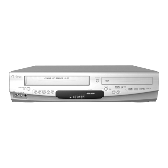
VIDEO CASSETTE RECORDER
DVD PLAYER &
DPVR-7630
When servicing the deck
mechanism, refer to MK14 Deck
Mechanism Section.
Deck Mechanism Part No.:
N25E0FL
Bar code Label
U
-E8D00ED
"
"
E8D00ED
PAL
Advertisement
Table of Contents

Related Manuals for FUNAI DPVR-7630


Summary of Contents for FUNAI DPVR-7630
- Page 1 Deck Mechanism Part No.: I CBA’s I Exploded views N25E0FL I Parts List This service manual is for the DPVR-7630 different DVD Main CBA UNIT model, which Bar code Label is different from the previous model. For the DPVR-7630 different DVD Main CBA...
-
Page 2: Table Of Contents
MAIN SECTION DVD PLAYER & VIDEO CASSETTE RECORDER DPVR-7630 Main Section I Specifications I Preparation for Servicing I Adjustment Procedures I Schematic Diagrams I CBA’s I Exploded Views I Parts List TABLE OF CONTENTS Specifications ............... . . 1-1-1 Laser Beam Safety Precautions . -
Page 3: Specifications
SPECIFICATIONS < VCR Section > Description Unit Minimum Nominal Maximum Remark 1. Video 1-1. Video Output (PB) Vp-p SP Mode 1-2. Video Output (R/P) Vp-p SP Mode, 1-3. Video S/N Y (R/P) W/O Burst 1-4. Video Color S/N AM (R/P) SP Mode 1-5. - Page 4 < DVD Section > ITEM CONDITIONS UNIT NOMINAL LIMIT 75 Ω load 1. Video Output ± 0.1 2. Optical Digital Out 3. Audio (PCM) 1 kHz 0 dB, 47k Ω load 3-1. Output Level Vrms 47k Ω load 3-2. S/N 3-3.
-
Page 5: Laser Beam Safety Precautions
LASER BEAM SAFETY PRECAUTIONS This DVD player uses a pickup that emits a laser beam. Do not look directly at the laser beam coming from the pickup or allow it to strike against your skin. The laser beam is emitted from the location shown in the figure. When checking the laser diode, be sure to keep your eyes at least 30 cm away from the pickup lens when the diode is turned on. -
Page 6: Important Safety Precautions
IMPORTANT SAFETY PRECAUTIONS Product Safety Notice K. Crimp type wire connector The power transformer uses crimp type connectors Some electrical and mechanical parts have special which connect the power cord and the primary side safety-related characteristics which are often not evi- of the transformer. -
Page 7: Safety Check After Servicing
Safety Check after Servicing Examine the area surrounding the repaired location for damage or deterioration. Observe that screws, Chassis or Secondary Conductor parts, and wires have been returned to their original positions. Afterwards, do the following tests and con- Primary Circuit firm the specified values to verify compliance with safety standards. -
Page 8: Standard Notes For Servicing
STANDARD NOTES FOR SERVICING Circuit Board Indications Pb (Lead) Free Solder When soldering, be sure to use the Pb free solder. 1. The output pin of the 3 pin Regulator ICs is indi- cated as shown. How to Remove / Install Flat Pack-IC Top View Bottom View 1. - Page 9 3. The flat pack-IC on the CBA is affixed with glue, so With Soldering Iron: be careful not to break or damage the foil of each (1) Using desoldering braid, remove the solder from all pin or the solder lands under the IC when removing pins of the flat pack-IC.
- Page 10 2. Installation (4) Bottom of the flat pack-IC is fixed with glue to the CBA; when removing entire flat pack-IC, first apply (1) Using desoldering braid, remove the solder from soldering iron to center of the flat pack-IC and heat the foil of each pin of the flat pack-IC on the CBA up.
- Page 11 Instructions for Handling Semi-conductors Electrostatic breakdown of the semi-conductors may occur due to a potential difference caused by electro- static charge during unpacking or repair work. 1. Ground for Human Body Be sure to wear a grounding band (1MΩ) that is prop- erly grounded to remove any static electricity that may be charged on the body.
-
Page 12: Preparation For Servicing
PREPARATION FOR SERVICING How to Enter the Service Mode About Optical Sensors Caution: An optical sensor system is used for the Tape Start and End Sensors on this equipment. Carefully read and follow the instructions below. Otherwise the unit may operate erratically. What to do for preparation Insert a tape into the Deck Mechanism Assembly and press the PLAY button. -
Page 13: Cabinet Disassembly Instructions
CABINET DISASSEMBLY INSTRUCTIONS 1. Disassembly Flowchart REMOVAL This flowchart indicates the disassembly steps to gain REMOVE/*UNHOOK/ LOC. PART Fig. access to item(s) to be serviced. When reassembling, UNLOCK/RELEASE/ Note follow the steps in reverse order. Bend, route, and UNPLUG/DESOLDER dress the cables as they were originally. 5(S-8), 2(S-9), (S-10), [1] Top Case Chassis Unit... - Page 14 Reference Notes CAUTION 1: Locking Tabs (L-1) and (L-2) are fragile. Be careful not to break them. (S-1) (S-1) 1-1. Release three Locking Tabs (L-1). [1] Top Case 1-2. Release three Locking Tabs (L-2), then remove the Front Assembly. CAUTION 2: Electrostatic breakdown of the laser (S-1) diode in the optical system block may occur as a potential difference caused by electrostatic charge...
- Page 15 CN401 (S-3) CN601 (S-9) (S-8) (S-3) (S-8) [4] DVD Mechanism (S-9) Assembly (S-3) (S-4) [5] Partition Plate (S-8) (S-5) (S-6) CN501 (S-10) [9] VCR Chassis Unit [7] Loader Holder [6] Power Supply CBA (L-3) Fig. D5 Fig. D3 (S-7) (S-7) [8] DVD Main CBA Unit CN301...
- Page 16 Cylinder Assembly FE Head ACE Head Assembly [10] Deck Assembly SW507 Lead with blue stripe LD-SW [13] Jack-A CBA (S-11) (S-13) [12] Main CBA [10] Deck Assembly (S-13) Cam Gear [12] Main CBA Desolder (S-11) Hole Shaft from bottom [11] DVD (S-12) Open/Close CBA Hole...
- Page 17 HOW TO EJECT MANUALLY 1. Remove the Top Case, Front Assembly and Top Bracket. 2. Remove four Screws (S-3) in Fig. D3. Do not disconnect connectors. 3. While lifting up the DVD Mechanism, rotate the roulette in the direction of the arrow as shown below.
-
Page 18: Electrical Adjustment Instructions
ELECTRICAL ADJUSTMENT INSTRUCTIONS General Note: "CBA" is an abbreviation for 3. To check/reset the initial function "Circuit Board Assembly." setting NOTE: Preparation: Electrical adjustments are required after replacing 1. Enter the service mode. circuit components and certain mechanical parts. It is important to do these adjustments only after all repairs 2. -
Page 19: How To Initialize The Dvd Player & Vcr
HOW TO INITIALIZE THE DVD PLAYER & VCR To put the program back at the factory-default, initialize the DVD player & VCR as the following procedure. < DVD Section > 1. Press [DVD], [1], [2], [3], [4], and [DISPLAY] buttons on the remote control unit in that order. Fig. -
Page 20: Firmware Renewal Mode
FIRMWARE RENEWAL MODE 1. Turn the power on and remove the disc on the tray. 5. After programming is finished, the tray opens automatically. Fig. e appears on the screen and 2. To put the DVD player into version up mode, press the checksum in (*2) of Fig. - Page 21 10. Press [CLEAR] button on the remote control unit. Fig. h appears on the screen. " ******* " differs depending on the models. MODEL : ******* Version : *.** Region : * EEPROM CLEAR : OK EEPROM CLEAR : CLEAR EXIT: POWER Fig.
-
Page 22: Function Indicator Symbols
FUNCTION INDICATOR SYMBOLS Note: If a mechanical malfunction occurs, the power is turned off. When the power comes on again after that by pressing [STANDBY-ON] button, an error message is displayed on the TV screen for 5 seconds. MODE INDICATOR ACTIVE When reel or capstan mechanism is not “A R”... -
Page 23: Block Diagrams
BLOCK DIAGRAMS <VCR SECTION> Servo / System Control Block Diagram E8D00BLS 1-11-1... - Page 24 Video Block Diagram E8D00BLV 1-11-2...
- Page 25 Audio Block Diagram E8D00BLA 1-11-3...
- Page 26 Hi-Fi Audio Block Diagram E8D00BLH 1-11-4...
- Page 27 Power Supply Block Diagram E8D00BLP 1-11-5...
- Page 28 BLOCK DIAGRAMS <DVD SECTION> DVD System Control / Servo Block Diagram E8D00BLSD 1-11-6...
- Page 29 Digital Signal Process Block Diagram E8D00BLD 1-11-7...
- Page 30 DVD Video / Audio Block Diagram 1-11-8 E8D00BLVD...
-
Page 31: Schematic Diagrams / Cba's And Test Points
SCHEMATIC DIAGRAMS / CBA’S AND TEST POINTS Standard Notes WARNING Many electrical and mechanical parts in this chassis have special characteristics. These characteristics often pass unnoticed and the protection afforded by them cannot necessarily be obtained by using replacement components rated for higher voltage, wattage, etc. - Page 32 LIST OF CAUTION, NOTES, AND SYMBOLS USED IN THE SCHEMATIC DIAGRAMS ON THE FOLLOWING PAGES: 1. CAUTION: FOR CONTINUED PROTECTION AGAINST FIRE HAZARD, REPLACE ONLY WITH THE SAME TYPE FUSE. 2. CAUTION: Fixed Voltage (or Auto voltage selectable) power supply circuit is used in this unit. If Main Fuse (F1001) is blown, first check to see that all components in the power supply circuit are not defec- tive before you connect the AC plug to the AC power supply.
- Page 33 Main 1/8 Schematic Diagram < VCR Section > 1-12-3 E8D00SCM1...
- Page 34 Main 2/8 & Sensor Schematic Diagram < VCR Section > IC611 MATRIX CHART SACD PSCAN REPEAT SACD PSCAN REPEAT TITLE GROUP GROUP TITLE HD VCD 1-12-4 E8D00SCM2...
- Page 35 Main 3/8 Schematic Diagram < VCR Section > 1-12-5 E8D00SCM3...
- Page 36 Main 4/8 Schematic Diagram < VCR Section > 1-12-6 E8D00SCM4...
- Page 37 Main 5/8 Schematic Diagram < VCR Section > 1-12-7 E8D00SCM5...
- Page 38 Main 6/8 Schematic Diagram < VCR Section > 1-12-8 E8D00SCM6...
- Page 39 1-12-9...
- Page 40 DVD Open/Close DVD Open/Close AFV CBA Bottom View AFV CBA Top View CBA Top View CBA Bottom View BE8B00F01013C BE6800F01091 Jack -A CBA Bottom View Jack -A CBA Top View BE8B00F01021C 1-12-19...
- Page 41 Power Supply CBA Top View Power Supply CBA Bottom View CAUTION ! Because a hot chassis ground is present in the power CAUTION ! supply circut, an isolation transformer must be used. For continued protection against fire hazard, Fixed voltage (or Auto voltage selectable) power supply circuit is used in this unit. replace only with the same type fuse.
-
Page 42: Waveforms
WAVEFORMS NOTE: Input COLOR BAR SIGNAL (WITH 1KHz AUDIO SIGNAL) TP301 UPPER TP504 Pin 8 of CN1601 Pin 12 of CN1601 LOWER C-PB 0.2V DVD-AUDIO(L) 0.5ms RF-SW VIDEO-Y 0.2V 20µs TP751 UPPER TP504 Pin 10 of CN1601 Pin 14 of CN1601 LOWER V-OUT 0.5V... -
Page 43: Wiring Diagram < Vcr Section
WIRING DIAGRAM < VCR SECTION > 1-14-1 E8D00WI... -
Page 44: Wiring Diagram < Dvd Section
WIRING DIAGRAM < DVD SECTION > 1-14-2 E8D00WID... -
Page 45: Ic Pin Function Descriptions
IC PIN FUNCTION DESCRIPTIONS < VCR Section > Signal Active Function Name Level IC501( SERVO / SYSTEM CONTROL IC ) Not Used “H” ≥ 4.5V, “L” ≤ 1.0V SCART 2 RGB 27 OUT RGB Through Control THROUGH Signal Active Signal Function Name Level... - Page 46 Signal Active Signal Active Function Function Name Level Name Level Not Used 83 OUT AUDIO- Audio Mute Control MUTE-H Signal (Mute = “H”) Not Used Not Used Not Used Not Used Composite PULSE C-SYNC Synchronized Hi-Fi Tape A-MODE Pulse Detection Signal Control SCART 1 Capstan Motor 8Pin Level by...
- Page 47 IC612 ( FIP DRIVER ) Signal Name Function Name FP-CLK Clock Input FP-STB Serial Interface Strobe Not Used Not Used Power Supply Segment Output Pull Down Level Segment Output Grid Output Power Supply Oscillator Input Not Used FP-DIN Serial Data Input 1-15-3 E8D04PIN...
-
Page 48: Lead Identifications
LEAD IDENTIFICATIONS KRA103M-AT/P 2SA1015-GR(TE2 F T) MID-32A22F 2SK3566 KRC103M-AT/P 2SA1020-Y(TE6 F M) PT204-6B-12 KTA1266-GR-AT/P 2SA1815-(BL,GR,Y)(TE2 F T) KTA1267-(GR,Y)-AT/P 2SC2120-Y(TE2 F T) KTC3199-(BL,GR,Y)-AT/P 2SC3266-Y(TPE2 F) RN2204(TE4 F T) KTA1281Y-AT/P KTC3203-Y-AT/P KTC3205-Y-AT/P G D S E C B E C B KIA4558P/P KRC103S-RTK/P FMG4A T148 EL817A... -
Page 49: Exploded Views
EXPLODED VIEWS Cabinet 2L071 2L071 2B21 2L071 See Electrical Parts List 2L012 for parts with this mark. 2L021 2L021 2L071 Some Ref. Numbers are 2L021 not in sequence. L0-9 L0-9 2L082 JW004 2L020 Jack-A CBA 2L021 JW003 Sensor CBA DVD Main AFV CBA CBA Unit 2B11... - Page 50 Packing X20A X20B X20C Some Ref. Numbers are not in sequence. Unit 1-17-2 E8D00PEX...
-
Page 51: Mechanical Parts List
MECHANICAL PARTS LIST PRODUCT SAFETY NOTE: Products marked with a ! have special characteristics important to safety. Before replacing any of these components, read carefully the product safety notice in this service manual. Don't degrade the safety of the product through improper servicing. -
Page 52: Electrical Parts List
ELECTRICAL PARTS LIST PRODUCT SAFETY NOTE: Products marked with a Ref. No. Description Part No. ! have special characteristics important to safety. C122 ELECTROLYTIC CAP . 1µF/50V M H7 or CE1JMAVSL1R0 Before replacing any of these components, read ALUMINUM ELECTROLYTIC CAP 1µF/50V H7 CE1JMAVSM1R0 carefully the product safety notice in this service C123 ELECTROLYTIC CAP . - Page 53 Ref. No. Description Part No. Ref. No. Description Part No. C324 CHIP CERAMIC CAP .(1608) B K 0.01µF/50V CHD1JK30B103 C418 CHIP CERAMIC CAP .(1608) F Z 0.1µF/50V or CHD1JZ30F104 C325 CHIP CERAMIC CAP . B K 8200pF/50V CHD1JK30B822 CHIP CERAMIC CAP .(1608) F Z 0.1µF/25V CHD1EZ30F104 C326 CHIP CERAMIC CAP .(1608) F Z 0.1µF/50V or...
- Page 54 Ref. No. Description Part No. Ref. No. Description Part No. ALUMINUM ELECTROLYTIC CAP 4.7µF/25V CE1EMAVSM4R7 CHIP CERAMIC CAP .(1608) B K 0.1µF/16V CHD1CK30B104 C612 CHIP CERAMIC CAP .(1608) B K 4700pF/50V CHD1JK30B472 C485 ELECTROLYTIC CAP . 10µF/16V M H7 or CE1CMAVSL100 C614 CHIP CERAMIC CAP .(1608) F Z 0.1µF/50V or...
- Page 55 Ref. No. Description Part No. Ref. No. Description Part No. C1355 CHIP CERAMIC CAP . F Z 1µF/10V or CHD1AZB0F105 D110 ZENER DIODE MTZJT-7711A or QDTA00MTZJ11 CHIP CERAMIC CAP . F Z 1µF/10V CHD1AZ30F105 DIODE ZENER 11BSA-T26 or NDTA011BST26 C1359 CHIP CERAMIC CAP .
- Page 56 Ref. No. Description Part No. Ref. No. Description Part No. IC1002 VOLTAGE REGULATOR PQ1LAX95MSPQ QSZBA0TSH053 CHIP TRANSISTOR FMG4A T148 QQ2Z000FMG4A IC1003 VOLTAGE REGULATOR PQ1LAX95MSPQ QSZBA0TSH053 Q403 TRANSISTOR KTC3203-Y-AT/P or NQSYKTC3203P IC1201 IC OP AMP KIA4558P/P or NSZBA0SJY035 TRANSISTOR 2SC2120-Y(TE2 F T) QQSY2SC2120F IC OP AMP RC4580IP or NSZBA0STY173...
- Page 57 Ref. No. Description Part No. Ref. No. Description Part No. CARBON RES. 1/4W J 1.2 k Ω CHIP RES. 1/10W J 470 Ω or R060 RCX4JATZ0122 R321 RRXAJR5Z0471 CARBON RES. 1/4W J 8.2 k Ω RES CHIP 1608 1/10W J 470 Ω R061 RCX4JATZ0822 RRXA471YF002...
- Page 58 Ref. No. Description Part No. Ref. No. Description Part No. CHIP RES. 1/10W J 4.7 k Ω or RES CHIP 1608 1/10W J 100 Ω R420 RRXAJR5Z0472 RRXA101YF002 RES CHIP 1608 1/10W J 4.7 k Ω CHIP RES. 1/10W J 33 Ω or RRXA472YF002 R481 RRXAJR5Z0330...
- Page 59 Ref. No. Description Part No. Ref. No. Description Part No. CARBON RES. 1/4W J 10 k Ω RES CHIP 1608 1/10W J 1.0 k Ω R545 RCX4JATZ0103 RRXA102YF002 CHIP RES. 1/10W J 1 k Ω or CARBON RES. 1/4W J 1 k Ω R546 RRXAJR5Z0102 R706...
- Page 60 Ref. No. Description Part No. Ref. No. Description Part No. CHIP RES. 1/10W F 12 k Ω or CHIP RES. 1/10W J 6.8 k Ω or R1206 RRXAFR5H1202 R1503 RRXAJR5Z0682 CHIP RES.(1608) 1/10W F 12 k Ω or RES CHIP 1608 1/10W J 6.8 k Ω RRXAFR5Z1202 RRXA682YF002 RES CHIP 1608 1/10W F 12.0 k Ω...
- Page 61 Ref. No. Description Part No. Ref. No. Description Part No. JK754 RCA JACK 1P MSP-281V31-A(B110) JYRL010LY027 ALUMINUM ELECTROLYTIC CAP 1000µF/16V CE1CMZPTM102 JK1202 RCA JACK MSP-281V41-B(B110) JXRL010LY140 C018 ELECTROLYTIC CAP . 470µF/6.3V M or CE0KMASDL471 JK1401 S TYPE JACK MDC-050V-2.4 LF(B110 or JXEL040LY003 ELECTROLYTIC CAP .
- Page 62 Ref. No. Description Part No. Ref. No. Description Part No. D1012 SWITCHING DIODE 1SS133(T-77) or QDTZ001SS133 TRANSISTOR KTA1267-GR-AT/P NQS1KTA1267P DIODE SWITCHING 1N4148-F0021 or NDTZ01N4148F Q1008 TRANSISTOR KTC3199-Y-AT/P or NQSYKTC3199P SWITCHING DIODE 1N4148M NDTZ01N4148M TRANSISTOR KTC3199-GR-AT/P or NQS4KTC3199P D1016 RECTIFIER DIODE FR101 NDWZ000FR101 TRANSISTOR 2SC1815-Y(TE2 F T) or QQSY2SC1815F...
- Page 63 JUNCTION CBA Ref. No. Description Part No. CARBON RES. 1/6W J 4.7 k Ω or R125 RCX6JATZ0472 Ref. No. Description Part No. CARBON RES. 1/4W J 4.7 k Ω RCX4JATZ0472 JUNCTION CBA (PSV-B) ---------- CHIP RES. 1/10W J 75 Ω or R126 RRXAJR5Z0750 Consists of the following:...
- Page 64 Ref. No. Description Part No. CHIP RES. 1/10W J 120 k Ω or RRXAJR5Z0124 RES CHIP 1608 1/10W J 120 k Ω RRXA124YF002 CHIP RES.(1608) 1/10W 0 Ω or RRXAZR5Z0000 RES CHIP 1608 1/10W J 0 Ω RRXA000YF002 CHIP RES.(1608) 1/10W 0 Ω or RRXAZR5Z0000 RES CHIP 1608 1/10W J 0 Ω...
- Page 65 DPVR-7630 E8D00ED 2006-09-21...