Table of Contents
Advertisement
SERVICE MANUAL
Main Section
I Specifications
I Preparation for Servicing
I Adjustment Procedures
I Schematic Diagrams
I CBA's
I Exploded views
I Parts List
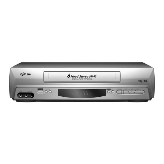
VIDEO CASSETTE RECORDER
When servicing the deck
mechanism, refer to MK14 Deck
Mechanism Section.
Deck Mechanism Part No.:
N25E0FL
31B-750
31A-850
PAL
Advertisement
Table of Contents

Related Manuals for FUNAI 31B-750


Summary of Contents for FUNAI 31B-750
- Page 1 When servicing the deck Main Section I Specifications mechanism, refer to MK14 Deck I Preparation for Servicing Mechanism Section. I Adjustment Procedures I Schematic Diagrams Deck Mechanism Part No.: I CBA’s I Exploded views N25E0FL I Parts List VIDEO CASSETTE RECORDER 31B-750 31A-850...
-
Page 2: Table Of Contents
MAIN SECTION VIDEO CASSETTE RECORDER 31B-750/31A-850 Sec. 1: Main Section I Specifications I Preparation for Servicing I Adjustment Procedures I Schematic Diagrams I CBA’s I Exploded Views I Parts List TABLE OF CONTENTS Specifications ............... . . 1-1-1 Important Safety Precautions . -
Page 3: Specifications
SPECIFICATIONS Description Unit Minimum Nominal Maximum Remark 1. Video 1-1. Video Output (PB) Vp-p FL6A 1-2. Video Output (R/P) Vp-p SP Mode, 1-3. Video S/N Y (R/P) W/O Burst 1-4. Video Color S/N AM (R/P) SP Mode 1-5. Video Color S/N PM (R/P) SP Mode 1-6. -
Page 4: Important Safety Precautions
IMPORTANT SAFETY PRECAUTIONS Product Safety Notice K. Crimp type wire connector The power transformer uses crimp type connectors Some electrical and mechanical parts have special which connect the power cord and the primary side safety-related characteristics which are often not evi- of the transformer. -
Page 5: Safety Check After Servicing
Safety Check after Servicing Chassis or Secondary Conductor Examine the area surrounding the repaired location for damage or deterioration. Observe that screws, parts, and wires have been returned to their original Primary Circuit positions. Afterwards, do the following tests and con- firm the specified values to verify compliance with safety standards. -
Page 6: Standard Notes For Servicing
STANDARD NOTES FOR SERVICING Circuit Board Indications Pb (Lead) Free Solder 1. The output pin of the 3 pin Regulator ICs is When soldering, be sure to use the Pb free solder. indicated as shown. How to Remove / Install Flat Pack-IC Top View Bottom View 1. - Page 7 3. The flat pack-IC on the CBA is affixed with glue, so With Soldering Iron: be careful not to break or damage the foil of each 1. Using desoldering braid, remove the solder from pin or the solder lands under the IC when all pins of the flat pack-IC.
- Page 8 2. Installation With Iron Wire: 1. Using desoldering braid, remove the solder from 1. Using desoldering braid, remove the solder from all pins of the flat pack-IC. When you use solder the foil of each pin of the flat pack-IC on the CBA flux which is applied to all pins of the flat pack-IC, so you can install a replacement flat pack-IC more you can remove it easily.
- Page 9 Instructions for Handling Semi- conductors Electrostatic breakdown of the semi-conductors may occur due to a potential difference caused by electrostatic charge during unpacking or repair work. 1. Ground for Human Body Be sure to wear a grounding band (1 MΩ) that is properly grounded to remove any static electricity that may be charged on the body.
-
Page 10: Preparation For Servicing
PREPARATION FOR SERVICING How to Enter the Service Mode About Optical Sensors Caution: An optical sensor system is used for the Tape Start and End Sensors on this equipment. Carefully read and follow the instructions below. Otherwise the unit may operate erratically. What to do for preparation Insert a tape into the Deck Mechanism Assembly and press the PLAY button. -
Page 11: Cabinet Disassembly Instructions
CABINET DISASSEMBLY INSTRUCTIONS 1. Disassembly Flowchart (1): Identification (location) No. of parts in the figures (2): Name of the part This flowchart indicates the disassembly steps to gain (3): Figure Number for reference access to item(s) to be serviced. When reassembling, (4): Identification of parts to be removed, unhooked, follow the steps in reverse order. - Page 12 (L-2) [4] Jack CBA (L-2) (S-5) Desolder [2] Front Assembly Fig. D4 (L-1) Fig. D2 (S-2) (S-2) (S-3) (S-2) (S-3) (S-4) [3]VCR Chassis (S-3) Unit (S-2) Fig. D3 1-5-2 HM4N0DC...
- Page 13 [7] Cylinder Shield Cylinder Assembly FE Head (S-7) SW507 ACE Head LD-SW Assembly [6] Main CBA [5] Deck [5] Deck Assembly [8] Jack Board Assembly (L-3) Cam Gear Hole Shaft Hole [6] Main CBA LD-SW [6] Main CBA (S-6) Fig. D6 (S-6) TOP VIEW From...
-
Page 14: Electrical Adjustment Instructions
ELECTRICAL ADJUSTMENT INSTRUCTIONS General Note: "CBA" is an abbreviation for Head Switching Position Adjustment "Circuit Board Assembly." Purpose: NOTE: To determine the Head Switching position during 1.Electrical adjustments are required after replacing playback. circuit components and certain mechanical parts. Symptom of Misadjustment: It is important to do these adjustments only after all repairs and replacements have been com- May cause Head Switching noise or vertical jitter... -
Page 15: How To Initialize The Vcr
HOW TO INITIALIZE THE VCR To put the program back at the factory-default, initialize the VCR as the following procedure. 1. Make sure that no timer programming is set. If not, reset all timer programming. 2. Turn the power off. 3. -
Page 16: Function Indicator Symbols
FUNCTION INDICATOR SYMBOLS Note: The following symbols will appear on the indicator panel to indicate the current mode or operation of the VCR. On-screen modes will also be momentarily displayed on the tv screen when you press the operation buttons. Display panel MODE INDICATOR ACTIVE... - Page 17 TV screen Note: OSD for mechanical error will be displayed for 5 sec. after the mechanical error occurs. Cause Indicator Active When reel or capstan mechanism is not “A R” is displayed on a TV screen. (Refer to Fig. 1.) functioning correctly When tape loading mechanism is not “A T”...
-
Page 18: Block Diagrams
BLOCK DIAGRAMS Servo / System Control Block Diagram HM410BLS 1-9-1... - Page 19 Video Block Diagram HM410BLV 1-9-2...
- Page 20 Audio Block Diagram HM410BLA 1-9-3...
- Page 21 Hi-Fi Audio Block Diagram HM410BLH 1-9-4...
- Page 22 Power Supply Block Diagram HM410BLP 1-9-5...
-
Page 23: Schematic Diagrams / Cba's And Test Points
SCHEMATIC DIAGRAMS / CBA’S AND TEST POINTS Standard Notes WARNING Many electrical and mechanical parts in this chassis have special characteristics. These characteristics often pass unnoticed and the protection afforded by them cannot necessarily be obtained by using replacement components rated for higher voltage, wattage, etc. - Page 24 LIST OF CAUTION, NOTES, AND SYMBOLS USED IN THE SCHEMATIC DIAGRAMS ON THE FOLLOWING PAGES: 1. CAUTION: FOR CONTINUED PROTECTION AGAINST FIRE HAZARD, REPLACE ONLY WITH THE SAME TYPE FUSE. 2. CAUTION: Fixed Voltage (or Auto voltage selectable) power supply circuit is used in this unit. If Main Fuse (F001) is blown, first check to see that all components in the power supply circuit are not defective before you connect the AC plug to the AC power supply.
- Page 25 Main 1/6 Schematic Diagram Comparison Chart of Models and Marks MODEL MARK 31B-750 31B-850 1-10-3 HM410SCM1...
- Page 26 Main 2/6 & Sensor Schematic Diagram FP562 MATRIX CHART 1-10-4 HM410SCM2...
- Page 27 Main 3/6 Schematic Diagram 1-10-5 HM410SCM3...
- Page 28 Main 4/6, Jack & Sub Jack Schematic Diagram 1-10-6 HM410SCM4...
- Page 29 Main 5/6 Schematic Diagram NOTE: CAUTION ! CAUTION ! For continued protection against fire hazard, The voltage for parts in hot circuit is measured using Fixed voltage (or Auto voltage selectable) power supply circuit is used in this unit. hot GND as a common terminal. If Main Fuse (F001) is blown , check to see that all components in the power supply replace only with the same type fuse.
- Page 30 Main 6/6 Schematic Diagram 1-10-8 HM410SCM6...
- Page 31 AFV Schematic Diagram HM410SCAFV 1-10-9...
- Page 32 Main CBA Top View CAUTION ! Because a hot chassis ground is present in the power CAUTION ! For continued protection against fire hazard, Fixed voltage (or Auto voltage selectable) power supply circuit is used in this unit. supply circut, an isolation transformer must be used. If Main Fuse (F001) is blown , check to see that all components in the power supply Also, in order to have the ability to increase the input replace only with the same type fuse.
- Page 33 Main CBA Bottom View CAUTION ! Because a hot chassis ground is present in the power CAUTION ! For continued protection against fire hazard, Fixed voltage (or Auto voltage selectable) power supply circuit is used in this unit. supply circut, an isolation transformer must be used. If Main Fuse (F001) is blown , check to see that all components in the power supply Also, in order to have the ability to increase the input replace only with the same type fuse.
- Page 34 Jack CBA Top View Jack CBA Bottom View 1-10-12 BHM450F01011C...
- Page 35 AFV CBA Top View AFV CBA Bottom View BE6800F01091 Sub Jack CBA Top View Sub Jack CBA Bottom View BHM450F01011B 1-10-13...
-
Page 36: Waveforms
WAVEFORMS NOTE: Input VCR: COLOR BAR SIGNAL (WITH 1KHz AUDIO SIGNAL) (WF1~WF3) TP301 UPPER TP502 LOWER C-PB 10mV x 10 RF-SW 0.5V x 10 UPPER TP502 LOWER V-OUT 0.1V x 10 RF-SW 0.5V x 10 50µs V-OUT E-E 10µs 50mV x 10 U31PWF 1-11-1... -
Page 37: Wiring Diagram
WIRING DIAGRAM 1-12-1 HM410WI... -
Page 38: Ic Pin Function Descriptions
IC PIN FUNCTION DESCRIPTIONS Signal Active Function Name Level IC501( SERVO / SYSTEM CONTROL IC ) Not Used “H” ≥ 4.5V, “L” ≤ 1.0V Not Used Signal Active Function Name Level Not Used Input Signal from Pin IN SC2-IN LINE- Audio Mute Control 8 of SCART2 28 OUT... - Page 39 Signal Active Signal Active Function Function Name Level Name Level LPF Connected A-MUTE- Audio Mute Control 83 OUT Terminal (Slicer) Signal Not Used Not Used Not Used Not Used Not Used P-DOWN- Power Voltage Down Detector Signal Composite IN C-SYNC PULSE Synchronized Pulse Capstan Motor...
-
Page 40: Lead Identifications
LEAD IDENTIFICATIONS KRA103M-AT/P 2SA1015-GR(TE2 F T) PT6958-FN-TP(L) KRC103M-AT/P 2SA1020-Y(TE6 F M) SC16458G KTA-1266-GR-AT/P 2SC1815-(BL,GR,Y)(TE2 F T) KTA1267-(GR,Y)-AT/P 2SC2120-Y(TE2 F T) KTC3199-(BL,GR,Y)-AT/P 2SC3266-Y(TPE2 F) RN2204(TE4 F T) KTA1281Y-AT/P KTC3203-Y-AT/P KTC3205-Y-AT/P E C B E C B BR24L02F-WE2 MID-32A22F 2SK3566 LTV-817-BF CAT24WC02WI-TE13 PT204-6B-12 PS2561A-1(Q,W) EL817(A,B) -
Page 41: Exploded Views
EXPLODED VIEWS Front Panel [ A ] [ B ] Comparison Chart of Models and Marks Model Mark 31B-750 31A-850 1-15-1 HM410FEX... - Page 42 2L011 2L011 See Electrical Parts List for parts with this mark. Some Ref. Numbers are not in sequence. 2L011 Comparison Chart of Models and Marks Model Mark 31B-750 JACK CBA 31A-850 2L011 2L012 2L022 2L042 2L021 2L021 2L021 2L051 2L021...
- Page 43 Packing [ A ] [ B ] X20A X20B X20C X20D X20E X20F X20G Some Ref. Numbers are not in sequence. [ A ] Unit Comparison Chart of Models and Marks Model Mark 31B-750 31A-850 1-15-3 HM410PEX...
-
Page 44: Mechanical Parts List
X20E! OWNERS MANUAL(SP) HM451ED 1VMN22157 X20F! OWNERS MANUAL(PO) HM451ED 1VMN22158 Model Mark X20G! OWNERS MANUAL(GE) HM451ED 1VMN22159 31B-750 QUICK GUIDE HM452BD 1VMN22161 31A-850 Ref. No. Mark Description Part No. FRONT ASSEMBLY HM410BD 1VM222235 FRONT ASSEMBLY HE450ED 0VM204197 CASE TOP(ANTHRACITE) HE240ED... -
Page 45: Electrical Parts List
Comparison Chart of Models and Marks C060 ELECTROLYTIC CAP . 10µF/16V M H7 or CE1CMAVSL100 Model Mark ALUMINUM ELECTROLYTIC CAP 10µF/ CE1CMAVSM100 16V H7 31B-750 C061 CHIP CERAMIC CAP .(1608) F Z 0.1µF/ CHD1JZ30F104 31A-850 50V or CHIP CERAMIC CAP .(1608) F Z 0.1µF/ CHD1EZ30F104... - Page 46 Ref. No. Mark Description Part No. Ref. No. Mark Description Part No. CHIP CERAMIC CAP .(1608) F Z 0.1µF/ CHD1EZ30F104 ALUMINUM ELECTROLYTIC CAP 1µF/ CE1JMAVSM1R0 50V H7 C314 CHIP CERAMIC CAP .(1608) B K 0.01µF/ CHD1JK30B103 C340 CHIP CERAMIC CAP . CH J 120pF/50V CHD1JJ3CH121 C341 CHIP CERAMIC CAP .
- Page 47 Ref. No. Mark Description Part No. Ref. No. Mark Description Part No. ALUMINUM ELECTROLYTIC CAP 10µF/ CE1CMAVSM100 C479 ELECTROLYTIC CAP . 4.7µF/25V M H7 or CE1EMAVSL4R7 16V H7 ALUMINUM ELECTROLYTIC CAP 4.7µF/ CE1EMAVSM4R7 C454 ELECTROLYTIC CAP . 22µF/10V M H7 or CE1AMAVSL220 25V H7 ALUMINUM ELECTROLYTIC CAP 22µF/ CE1AMAVSM220...
- Page 48 Ref. No. Mark Description Part No. Ref. No. Mark Description Part No. C528 CHIP CERAMIC CAP .(1608) B K 0.01µF/ CHD1JK30B103 DIODES D001 RECTIFIER DIODE 1N4005 or NDQZ001N4005 C530 CERAMIC CAP .(AX) F Z 0.022µF/25V CCA1EZTFZ223 RECTIFIER DIODE 1N4005 NDWZ001N4005 C531 CERAMIC CAP .(AX) Y M 0.01µF/16V CCA1CMT0Y103...
- Page 49 Ref. No. Mark Description Part No. Ref. No. Mark Description Part No. CHIP TRANSISTOR KTA1504S-GR-RTK/ NQ14KTA1504S IC001! PHOTOCOUPLER EL817A or NPEA000EL817 Q352 TRANSISTOR KTC3199-Y-AT/P or NQSYKTC3199P PHOTOCOUPLER EL817B or NPEB000EL817 TRANSISTOR KTC3199-GR-AT/P or NQS4KTC3199P PHOTOCOUPLER LTV-817B-F or NPEB0LTV817F TRANSISTOR 2SC1815-Y(TE2 F T) or QQSY2SC1815F PHOTOCOUPLER PS2561A-1(Q) or QPEQPS2561A1...
- Page 50 Ref. No. Mark Description Part No. Ref. No. Mark Description Part No. CARBON RES. 1/6W J 820 Ω or CHIP RES. 1/10W J 1.8k Ω R058 RCX6JATZ0821 R416 RRXAJR5Z0182 CARBON RES. 1/4W J 820 Ω CHIP RES. 1/10W J 560 Ω RCX4JATZ0821 R417 RRXAJR5Z0561...
- Page 51 Ref. No. Mark Description Part No. Ref. No. Mark Description Part No. CHIP RES. 1/10W J 33k Ω R533 RRXAJR5Z0333 TACT SWITCH TC-1104(H=9.5) SST0101DNG01 CARBON RES. 1/6W G 3.6k Ω or R534 RCX6GATZ0362 SW506 LEAF SWITCH MXS01830MVP0 SSC0101MCE03 CARBON RES. 1/4W G 3.6k Ω RCX4GATZ0362 SW507 ROTARY MODE SWITCH SSS-53MD...
- Page 52 JACK CBA Ref. No. Mark Description Part No. CARBON RES. 1/4W J 68 Ω R118 RCX4JATZ0680 Ref. No. Mark Description Part No. CHIP RES. 1/10W J 75 Ω R119 RRXAJR5Z0750 JACK CBA (MCV-C) ---------- CARBON RES. 1/6W J 680 Ω or R120 RCX6JATZ0681 Consists of the following:...
- Page 53 Ref. No. Mark Description Part No. CHIP CERAMIC CAP .(1608) F Z 0.1µF/ CHD1JZ30F104 50V or CHIP CERAMIC CAP .(1608) F Z 0.1µF/ CHD1EZ30F104 ELECTROLYTIC CAP . 10µF/16V M H7 or CE1CMASSL100 ELECTROLYTIC CAP . 10µF/16V M H7 CE1CMASSM100 ELECTROLYTIC CAP . 0.22µF/50V M H7 CE1JMASSLR22 ALUMINUM ELECTROLYTIC CAP CE1JMASSMR22...
- Page 54 31B-750/31A-850 HM410BD/451ED 2006-03-20...