Table of Contents
Troubleshooting

Related Manuals for Fluke 8842A


Summary of Contents for Fluke 8842A
-
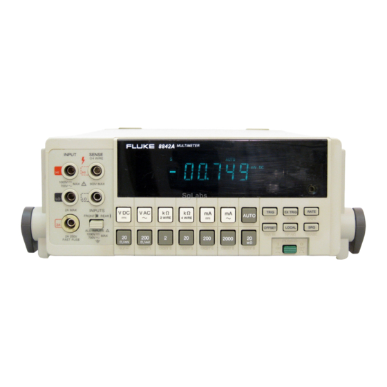
Page 1: Digital Multimeter
® 8842A Digital Multimeter Instruction Manual PN 879309 Date December 1991 Rev.3 7/96 © 1999 Fluke Corporation, All rights reserved. Printed in USA All product names are trademarks of their respective companies. -
Page 2: Table Of Contents
Table of Contents Chapter Title Page Introduction and Specifications............1-1 1-1. INTRODUCTION................1-2 1-2. THE 8842A DIGITAL MULTIMETER ..........1-2 1-3. OPTIONS AND ACCESSORIES ............1-2 1-4. SPECIFICATIONS ................1-3 Operating Instructions............... 2-1 2-1. INTRODUCTION................2-2 2-2. INSTALLATION ................. 2-2 2-3. - Page 3 8842A Instruction Manual 2-28. Current Fuse Protection..............2-13 2-29. Offset Measurements ............... 2-14 2-30. EXTERNAL CLEANING..............2-15 Remote Programming................ 3-1 3-1. INTRODUCTION................3-3 3-2. CAPABILITIES ................... 3-3 3-3. BUS SET-UP PROCEDURE ............... 3-3 3-4. AN OVERVIEW OF REMOTE OPERATION ........3-4 3-5.
- Page 4 Contents (continued) 3-50. The Serial Poll Register ..............3-27 3-51. The SRQ Mask................. 3-28 3-52. INTERFACE MESSAGES ..............3-29 3-53. Address Messages ................3-29 3-54. Universal Commands ............... 3-29 3-55. Addressed Commands..............3-30 3-56. TALK-ONLY MODE ................3-30 3-57. REMOTE CALIBRATION..............3-31 3-58.
- Page 5 8842A Instruction Manual 5-15. OHMS CURRENT SOURCE .............. 5-12 5-16. OHMS PROTECTION................. 5-13 5-17. OHMS FUNCTIONS ................5-13 5-18. 2-Wire Ohms..................5-13 5-19. 4-Wire Ohms..................5-15 5-20. A/D CONVERTER ................5-15 5-21. Timing/Data Control ................ 5-17 5-22. Precision DAC ................. 5-18 5-23.
- Page 6 Contents (continued) 6-20. TOLERANCE CHECK ............... 6-18 6-21. AC CALIBRATION AT OTHER FREQUENCIES ....6-19 6-22. OPTIMIZING USE OF THE 5450A........... 6-19 6-23. Remote Calibration ................6-20 6-24. TIMING CONSIDERATIONS ........... 6-23 6-25. REMOTE ERASURE..............6-24 6-26. EXAMPLE CALIBRATION PROGRAM........6-24 6-27.
- Page 7 8842A Instruction Manual 8-5. Replacement Test Leads (TL70A) ........... 8-4 8-6. Deluxe Test Lead Kits (Y8134) ............8-4 8-7. Slim-Flex Test Leads (Y8140)............8-4 8-8. Temperature Probes (80T-150U, and 80TK.) ........8-4 8-9. RF Probes (85RF and 83RF)............8-4 8-10.
- Page 8 List of Tables Table Title Page 2-1. Error Codes ......................2-9 2-2. Input Overload Limits.................... 2-13 3-1. Status Data ......................3-11 3-2. Numeric Output Data Format ................3-25 3-8. Serial Poll Register ....................3-28 3-3. Immediate-Mode Commands for Various Controllers .......... 3-32 3-4.
- Page 9 8842A Instruction Manual 6-27. AC Signal Tracing ....................6-68 6-28. Truth Table for U804 and K2 ................6-69 7-1. 8842A Digital Multimeter..................7-5 7-2. A1 Main PCA ......................7-10 7-3. A2 Display PCA ....................7-14 8-1. Accessories ......................8-3 8-2.
- Page 10 List of Figures Figure Title Page 1-1. External Dimensions....................1-11 2-1. Line Voltage Selection Settings................2-2 2-2. Adjusting the Handle ..................... 2-3 2-3. Rack-Mount Kits....................2-3 2-4. Installing the Single Rack Mount Kit ..............2-4 2-5. Front Panel Features ....................2-5 2-6.
- Page 11 6-3. Calibration Functions..................... 6-12 6-4. Optimizing Use of the 5450A ................6-20 6-5. Example A/D Calibration Program................ 6-25 6-6. 8842A Disassembly ....................6-26 6-7. Front Panel Disassembly..................6-34 6-8. Removing the Display Window................6-35 6-9. U202 Pin Diagram ....................6-46 6-10.
- Page 12 Contents (continued) 9-7. IEEE-488 Interface PCA, Option -05 ..............9-15 9-8. True RMS AC PCA, Option -09................9-17...
- Page 13 8842A Instruction Manual...
-
Page 14: Introduction And Specifications
Chapter 1 Introduction and Specifications Title Page 1-1. INTRODUCTION................1-2 1-2. THE 8842A DIGITAL MULTIMETER ..........1-2 1-3. OPTIONS AND ACCESSORIES ............1-2 1-4. SPECIFICATIONS ................1-3... -
Page 15: Introduction
This manual provides complete operating instructions and service information for the 8842A. If you want to get started using your 8842A right away, proceed to the operating instructions in Section 2. If you intend to use the 8842A with the IEEE-488 Interface (Option -05), read Sections 2 and 3. -
Page 16: Specifications
Introduction and Specifications SPECIFICATIONS 1-4. SPECIFICATIONS Specifications for the 8842A are given in Table 1-1. External dimensions are shown in Figure 1-1. Table 1-1. Specifications DC VOLTAGE Input Characteristics FULL SCALE 5ñ RESOLUTION INPUT DIGITS RESISTANCE RANGE 5ñ DIGITS 4ñ DIGITS* 20 mV 19.9999 mV... - Page 17 20 volts or 2 times full scale whichever is greater, not to exceed 1000V. Reading rate-1/3 rdg / sec. in the 20 mV, 20Ω, 200 mA dc ranges Reading rate-1.25 rdg / sec. in the 20 mV, 20Ω, 200 mA dc ranges TRUE RMS AC VOLTAGE (OPTION 8842A-09) Input Characteristics RANGE FULL SCALE 5ñ...
- Page 18 Introduction and Specifications SPECIFICATIONS Accuracy NORMAL (s) READING RATE ....±(% of Reading + Number of Counts). For sinewave inputs ≥10,000 counts FREQUENCY 24 HOURS 23±1°C 90 DAY 23±5°C 1 YEAR 23±5°C 2 YEARS ±5°C 20-45 1.2 + 100 1.2 + 100 1.2 + 100 1.2 + 100 45-200...
- Page 19 8842A Instruction Manual CURRENT Input Characteristics RANGE FULL SCALE 5½ RESOLUTION DIGITS 5½ DIGITS 4½ DIGITS 200 mA 199.999 mA 1 µA 10 µA 2000 mA 1999.99 mA 10 µA 100 µA 4½ digits at the fastest reading rate. The 200mA range is available for dc current only.
- Page 20 Introduction and Specifications SPECIFICATIONS MEDIUM AND FAST READING RATES..In medium rate, add 50 counts to number of counts. In fast reading rate, for sinewave inputs ≥1000 (4½ digit mode) counts and frequencies >100 Hz, the accuracy is ±(0.4% of reading +30 (4½ digit mode) counts). NONSINUSOIDAL INPUTS ......For nonsinusoidal inputs ≥10,000 counts with frequency components ≤100 kHz, add the following % of reading to the accuracy specifications...
- Page 21 8842A Instruction Manual Accuracy NORMAL (S) READING RATE ....±(% of Reading + Number of Counts) RANGE 24 HOURS 23±1°C 90 DAY 23±5°C 1 YEAR 23±5°C 2 YEARS 23±1°C 20Ω 0.007 + 30 0.009 + 40 0.012 + 40 0.015 + 40 200Ω...
- Page 22 AUTORANGING The 8842A autoranges up to the highest ranges in all funtions, down to the 200 mV range in the VDC and VAC funtions, and down to the 200 Ω ranges in the ohms funtions. To select the 20 mV dc, 20Ω, or 200 mA dc range, press the respective range button (or send the respective range command, if using the IEEE-488 option).
- Page 23 Delay” on previous page.) If the delay is disabled by using the T3 or T4 command, then the delay is 1 ms±150 µs. When the 8842A is triggered with an IEEE-488 command (GET or ?), the automatic settling time delay begins after the trigger command has been processed and recognized.
- Page 24 Introduction and Specifications SPECIFICATIONS GENERAL COMMON MODE VOLTAGE....1000V dc or peak ac, or 700V rms ac from any input to earth. TEMPREATURE RANGE .......0 to 50°C operating, -40 to 70°C storage. HUMIDITY RANGE .........80% RH from 0 to 35°C, 70% to 50°C. WARMUP TIME ........1 hour to rated specifications.
-
Page 25: Operating Instructions
Chapter 2 Operating Instructions Title Page 2-1. INTRODUCTION................2-2 2-2. INSTALLATION .................2-2 2-3. Installing the Power-Line Fuse ............2-2 2-4. Connecting to Line Power..............2-2 2-5. Adjusting the Handle................2-3 2-6. Rack Mounting Kits .................2-3 2-7. OPERATING FEATURES ..............2-4 2-8. Power-Up Features................2-4 2-9. Front and Rear Panel Features ............2-4 2-10. -
Page 26: Introduction
SET TO THE POWER-LINE VOLTAGE IN OUR AREA. The 8842A can be configured to accept line power of 100, 120, 220, or 240V ac (+/-10%, 250V maximum) at 50, 60, or 400 Hz. The voltage must be selected by setting the rear panel LINE SET switches as shown in Figure 2-1. -
Page 27: Adjusting The Handle
2-6. Rack Mounting Kits You can mount the 8842A in a standard 19-inch rack panel using the accessory rack mounting kits shown in Figure 2-3. To install the Single Rack Mount Kit, remove the handle and handle mounting plates, and attach the rack ears with the screws provided (Figure 2-4). -
Page 28: Operating Features
2-7. OPERATING FEATURES 2-8. Power-Up Features When the 8842A is turned on, all display segments light up for about 2 seconds while the instrument performs an internal self-test of its digital circuitry. The 8842A then assumes the following configuration: VDC function •... -
Page 29: Front Panel Features
Note that the VAC and mA AC functions are available only with the True RMS AC option. If this option is absent, pressing the VAC and mA AC function buttons causes the 8842A to briefly display an error message (ERROR 30). FUNCTION BUTTONS:... - Page 30 8842A may indicate errors. OFFSET stores the displayed reading as an If the 8842A is in remote, LOCAL returns it to offset, which the 8842A subtracts from all local control. If the 8842A is in local, the...
-
Page 31: Rear Panel Features
4 WIRE TALK EXT TRIG SAMPLE SH1, AH1, T5, L4, SR1, RL1, ONLY 10V MAX COMPLETE DC1, DT1, PP0, C0, E1 240V JOHN FLUKE MFG. CO., INC. IEEE-05 LINE 220V EVERETT, WA MADE IN U.S.A. AC-09 120V 100V 1000V 300V MAX... -
Page 32: Display Features
The annunciators are explained in Figure 2-5. 2-11. Error Messages If the 8842A detects an operator error or an internal failure, it displays an error message for about 2-1/2 seconds and then resumes normal operation. During this time, the front panel buttons are ignored. -
Page 33: Error Codes
MEANING CODE ANALOG SELF-TEST ERRORS OPERATION ERRORS 200 VAC, Zero AC funtions availible only with 8842A-09 True RMS AC option. 700 VAC, Zero mA AC or mA DC funtion selected while REAR inputs selected. OFFSET selected with reading unavailible for mA AC, Zero overrange. -
Page 34: Overrange Indication
The inputs must be left disconnected while the self-tests are performed or the 8842A may indicate that errors are present. If the 8842A detects an error, it displays an error message for about 2-1/2 seconds. (Error codes 01 through 29 correspond to the self-tests.) If self-test errors are displayed even when the input terminals are disconnected, there may be a hardware problem in your 8842A. -
Page 35: Manual Range
8842A selects the nearest valid range. For example, if the 8842A is in the VDC function and you press the 20 MΩ button, the 8842A selects the 1000V range. -
Page 36: Automatic Settling Time Delay
Section 1. 2-21. Automatic Settling Time Delay When the external trigger mode is selected, the 8842A automatically inserts a delay after receiving a trigger signal, but before starting the first input sample. The delay is just long... -
Page 37: Making Measurements
DO NOTAPPLY INPUT POTENTIALS THAT EXCEED THE INPUT OVERLOAD LIMITS SHOWN IN TABLE 2-2. The 8842A is protected against input overloads up to the limits shown in Table 2-2. Exceeding these limits may damage the instrument and/or pose a shock hazard. -
Page 38: Offset Measurements
Note that the input overload limits are not changed by the use of the offset feature. However, the display flashes if the 8842A is in the 1000V dc or 700V ac ranges and the input exceeds 1000V dc or 700V ac, respectively. -
Page 39: External Cleaning
NEVER GET WATER INSIDE THE CASE. TO AVOID INSTRUMENT DAMAGE, NEVER APPLY SOLVENTS TO THE INSTRUMENT. Should the 8842A case require cleaning, wipe the instrument with a cloth that is lightly dampened with water or a mild detergent solution. 2-15... - Page 40 8842A Instruction Manual 2-16...
-
Page 41: Measurement Tutorial
Chapter 4 Measurement Tutorial Title Page 4-1. INTRODUCTION................4-2 4-2. DC VOLTAGE MEASUREMENT .............4-2 4-3. Circuit Loading Error...............4-2 4-4. Input Bias Current Error..............4-3 4-5. RESISTANCE MEASUREMENT ............4-4 4-6. 2-Wire Ohms..................4-4 4-7. Correcting for Test Lead Resistance in 2-Wire Ohms .....4-5 4-8. 4-Wire Ohms..................4-5 4-9. -
Page 42: Introduction
Instruction Manual 4-1. INTRODUCTION This section discusses considerations and techniques to help you use the 8842A effectively. Among other things, this section discusses sources of error which are an inherent part of the measurement process and which occur for all multimeters. By understanding why and when these errors occur, and by knowing how and when to correct for them, you can make accurate measurements with confidence. -
Page 43: Input Bias Current Error
Measurement Tutorial DC VOLTAGE MEASUREMENT The input impedance of the 8842A is 10 MΩ in the 200V and 1000V dc ranges, and is greater than 10,000 MΩ in the 20 mV, 200 mV, 2V, and 20V ranges. Therefore, for the 8842A, circuit loading error is less than 0.01% as long as the source impedance is less... -
Page 44: Resistance Measurement
Note that this procedure does not correct for circuit loading error. Also note that if input bias current error is not corrected for, it may be added to the circuit loading error. 4-5. RESISTANCE MEASUREMENT The 8842A allows you to measure resistance in both 2-wire and 4-wire configurations. Each has its benefits. 4-6. -
Page 45: Correcting For Test Lead Resistance In 2-Wire Ohms
In 2-wire ohms, the resistance of the test leads can introduce error when measuring low resistances. Typical test leads may add as much as 0.5Q to 2-wire ohms readings. With the 8842A, it is easy to correct for this error using the OFFSET button: 1. Select the 2-wire ohms function. -
Page 46: Ohms Test Current
8842A Instruction Manual f4-04.wmf Figure 4-4. Wire Ohms Measurement Table 4-1. Ohms Test Current RANGE TEST CURRENT FULL SCALE VOLTAGE 20Ω 1 mA 0.02V 200Ω 1 mA 0.2V 2 kΩ 1 mA 2.0V 20 kΩ 100 µA 2.0V 200 kΩ... -
Page 47: Applications Of The Ohms Functions
2 kΩ range (about 6V). 3. Disconnect the + test lead. 4. To test for leakage, select the VDC function and the 20V range (leave the 8842A in the medium reading rate), and measure the voltage that was stored on the capacitor during step 2. -
Page 48: A Precision Current Source
This voltage drop is called the burden voltage, and it is highest for full- scale measurements. The full-scale burden voltage for the 8842A is typically less than The burden voltage can present a significant error if the current source being measured is unregulated (i.e., not a true current source) and if the resistance of the fuse and shunt is a... -
Page 49: Reducing Thermal Voltages
Measurement Tutorial REDUCING THERMAL VOLTAGES f4-05.wmf Figure 4-5. Burden Voltage Error Calculation 4-14. REDUCING THERMAL VOLTAGES When making very low-level dc measurements, thermal voltages can present an additional source of error. Thermal voltages are the thermovoltaic potentials generated at the junction between dissimilar metals. Thermal voltages typically occur at binding posts and can be greater than 10 µV. -
Page 50: Ac Voltage And Current Measurement
8842A and rms-calibrated average-responding meters display the correct rms reading of 1.00000V (the dc component equals 0). However, consider the 2V (peak-to-peak) square wave. Both types of meter correctly measure the dc component (0V), but only the 8842A correctly measures the ac component (1.00000V). The average-responding meter measures 1.110V, which amounts to an 11% error. -
Page 51: Waveform Comparison Chart
Measurement Tutorial AC VOLTAGE AND CURRENT MEASUREMENT f4-06.wmf Figure 4-6. Waveform Comparison Chart Since average-responding meters have been in use for so long, you may have accumulated test or reference data based on them. The conversion factors in Figure 4-6 should help you convert between the two measurement methods. -
Page 52: Crest Factor
Figure 4-7. Typical Crest Factors for Various Waveforms The 8842A has a full-scale crest factor limit of 3.0 for the 20V and 700V ranges, and 6.0 for the other ranges. For full-scale input signals with a crest factor above these limits, dynamic range limitations can begin to cause large errors. -
Page 53: Combined Ac And Dc Measurements
Figure 4-8. Combined AC and DC Measurement 4-20. Combined AC and DC Measurements The 8842A can be used to evaluate the true rms value of waveforms such as the one shown in Figure 4-8, which includes both ac and dc components. First, measure the rms value of the ac component using the VAC function. -
Page 54: Making Accurate Measurements On The 20 Mv And 20Ω Ranges
Figure 4-9. f4-09.wmf Figure 4-9. Reduction of Zero-Input Error As long as the 8842A reading is 1,000 counts or more, readings will still be within specified accuracy. 4-23. MAKING ACCURATE MEASUREMENTS ON THE 20 mV AND 20 Ω RANGES... -
Page 55: Making Accurate High-Resistance Measurements
For accurate measurements, use short test leads and enclose the test leads and test circuit in a proper shield that is connected to the 8842A’s INPUT LO terminal. Pickup of slowly fluctuating noise can also be reduced by using the OFFSET feature as described in paragraph 4-7. -
Page 56: Leakage Resistance In High Resistance Measurement
8842A Instruction Manual f4-12.wmf Figure 4-12. Leakage Resistance in High Resistance Measurement 4-16... -
Page 57: Theory Of Operation
Chapter 5 Theory of Operation Title Page 5-1. INTRODUCTION................5-3 5-2. OVERALL FUNCTIONAL DESCRIPTION ........5-3 5-3. DETAILED CIRCUIT DESCRIPTION ..........5-4 5-4. DC SCALING ..................5-4 5-5. VDC Scaling ..................5-6 5-6. VDC Protection................5-7 5-7. mA DC Scaling ................5-7 5-8. - Page 58 8842A Instruction Manual 5-36. POWER SUPPLY ................5-25 5-37. IEEE-488 INTERFACE (OPTION -05)..........5-26 5-38. Out-Guard Microcomputer............... 5-26 5-39. Guard Crossing................. 5-26 5-40. Bus Interface Circuitry..............5-26 5-41. Signal Conditioning ................. 5-27 5-42. IEEE-488 Interface Power Supply ........... 5-27 5-43.
-
Page 59: Introduction
Section 10. 5-2. OVERALL FUNCTIONAL DESCRIPTION A functional block diagram of the 8842A is shown in Figure 5-1. The basic signal path flows from left to right across the center of the page. The input is sensed at the input... -
Page 60: Detailed Circuit Description
8842A Instruction Manual 5-3. DETAILED CIRCUIT DESCRIPTION The following paragraphs give a detailed circuit description of each of the functional blocks in Figure 5-1. For clarity, measurement ranges are referred to as r1, r2, r3, etc., where r1 is the lowest possible range, r2 the next higher range, and so on. Pins are designated by the respective integrated circuit (e.g., U101-7 for U101 pin 7). -
Page 61: Overall Functional Block Diagram
Theory of Operation DC SCALING f5-01.wmf Figure 5-1. Overall Functional Block Diagram... -
Page 62: Vdc Scaling
8842A Instruction Manual 5-5. VDC Scaling Scaling is performed in the VDC function by two precision resistors networks (Z301 and Z302). These components are configured by relay K301, switching transistor Q311, and quad analog switches U302A and U301B to provide the correct scaling for each range. -
Page 63: Vdc Protection
Theory of Operation DC SCALING In the 20 mV, 200 mV and and 2V ranges, the input voltage is applied directly to the T/H Amplifier via Q310, Q311, and U301B. In the 20 mV range, the T/H Amplifier has a gain of 100;... -
Page 64: Track/Hold Circuit
8842A Instruction Manual 5-9. TRACK/HOLD CIRCUIT The Track/Hold (T/H) circuit presents a stable voltage to the A/D Converter during the input period of the A/D conversion cycle. The circuit also provides a gain of 100 in the 20 mV, 20Ω and 200 mA ranges, and a gain of 10 in the 200 mV dc, 200Ω, and 2000 mA dc ranges. -
Page 65: Track/Hold Circuit Configurations
Theory of Operation TRACK/HOLD CIRCUIT f5-04.wmf Figure 5-4. Track/Hold Circuit Configurations... -
Page 66: Track Configuration
8842A Instruction Manual f5-05.wmf Figure 5-5. Timing Diagram for One A/D Cycle 5-10. Track Configuration In the track configuration (Figure 5-4A), the T/H circuit functions as a non-inverting buffer. The voltage on C308 tracks the scaled dc input voltage. 5-10... -
Page 67: Settling Configuration
Theory of Operation PRECISION VOLTAGE REFERENCE 5-11. Settling Configuration The circuit assumes a settling configuration between the track and hold configurations. The circuit assumes the configuration in Figure 5-4B for unity gain and the configuration in Figure 5-4C for gain of 10. During this time the DC Scaling circuit is still connected to the T/H amp. -
Page 68: Ohms Current Source
8842A Instruction Manual Resistor R701, precision resistor network Z701, and transistor/zener diode combination U701 are produced as a matched set so that the output of U702A is precisely -7.00000V. This output is remotely sensed at the pins of the custom A/D IC (U101). Diode CR701 prevents the output from going positive at power-up. -
Page 69: Ohms Protection
Theory of Operation OHMS PROTECTION The second stage (U404, precision resistor network Z401, and analog switches U402 and U403) is a current amplifier whose gain is controlled by the In-Guard µC. The In-Guard µC sets the output current for each range by controlling U402 and U403. (See switch state table in Figure 5-7.) 5-16. -
Page 70: Ohms Scaling
8842A Instruction Manual f5-08.wmf Figure 5-8. Ohms Scaling 5-14... -
Page 71: 4-Wire Ohms
2000 kΩ range and less than 100Ω in the 20 MΩ range. 5-20. A/D CONVERTER The Analog-to-Digital (A/D) Converter (Figure 5-9) uses Fluke’s patented recirculating remainder technique. An input voltage (Vin) is compared to the output of the precision Digital-to-Analog Converter (DAC). -
Page 72: Analog-To-Digital Converter
8842A Instruction Manual f5-09.wmf Figure 5-9. Analog-to-Digital Converter The conversion process is broken up into an autozero period followed by five measurement intervals. (A timing diagram is shown in Figure 5-5.) Six bits of the final A/D sample are obtained during each interval. -
Page 73: Timing/Data Control
Theory of Operation A/D CONVERTER f5-10.wmf Figure 5-10. First Remainder-Store Period This five-interval process thus generates five nibbles which are processed by the In- Guard µC to produce one A/D sample. After the fifth nibble is generated, U101 interrupts the In-Guard µC over line INT. The In-Guard µC then pulls line CS7 low five times, causing U101 to send the µC the five (six-bit) nibbles one-at-a-time over lines AD0- AD5. -
Page 74: A/D Amplifier
8842A Instruction Manual The bit-switches determine the output voltage of U102B by controlling the binary ladder network. The gain of U102B is set by the ratio of a precision feedback resistor (Z101-7, - 8) and the equivalent output resistance of the ladder network. -
Page 75: Keyboard
Theory of Operation KEYBOARD f5-12.wmf Figure 5-12. Vacuum Fluorescent Display The Digital Controller sequentially enables the G lines by applying +30V dc (nominal). When a G line is enabled, electrons flow from the filament to the enabled grid. If a P line is enabled (i.e., raised to a nominal +30V dc by the Digital Controller), the electrons continue past the grid and strike the respective plate, causing it to glow. -
Page 76: Digital Controller Block Diagram
8842A Instruction Manual f5-13.wmf Figure 5-13. Digital Controller Block Diagram 5-20... -
Page 77: In-Guard Microcomputer
Theory of Operation DIGITAL CONTROLLER 5-28. In-Guard Microcomputer The In-Guard Microcomputer (µC) is a single-chip Z8 microcomputer containing 4K bytes of ROM, 144 bytes of RAM, a UART, and four 8-bit I/O ports. It communicates with the rest of the instrument via the internal bus and dedicated I/O lines. The In-Guard µC is reset when pin 6 is pulled low either by C204 at power-up or by the watch-dog timer in the custom A/D IC (U101). -
Page 78: Read/Write Timing Diagrams For Internal Bus
8842A Instruction Manual f5-14.wmf Figure 5-14. Read/Write Timing Diagrams for Internal Bus 5-22... -
Page 79: Function And Range Control
Theory of Operation DIGITAL CONTROLLER 5-29. Function and Range Control The In-Guard µC configures the DC Scaling circuit, the Track/Hold circuit, and the Ohms Current Source to provide the proper input switching, scaling, and filtering for each function, range, and reading rate. It does this by controlling dedicated output lines which control relays and FET switches, and by sending configuration codes out on the bus. -
Page 80: Keyboard/Display Control
8842A Instruction Manual 5-32. Keyboard/Display Control Keyboard/Display Controller U212 communicates with the In-Guard µC over the internal bus. During a µC write cycle, address line A0 tells U212 whether to consider data being sent by the µC as configuration commands or as display data. Display data is stored in the Keyboard/Display Controller, which automatically scans the display. -
Page 81: Power Supply
AC voltage for the +15V and -15V supplies is rectified by bridge network CR608, CR609, CR610, and CR611 and regulated by VR603 and VR604. The +15V and -15V supply analog circuitry throughout the 8842A. Zener diodes CR613 and CR614 supply +7.5V and -8.2V to the A/D Converter, analog filter, and DC Scaling circuit. -
Page 82: Ieee-488 Interface (Option -05)
8842A Instruction Manual 5-37. IEEE-488 INTERFACE (OPTION -05) The IEEE-488 Interface has five major parts, as shown in the block diagram in Figure 5- 16. All components are contained in a single printed circuit assembly (PCA). Reference designations are numbered in the 900 series. -
Page 83: Signal Conditioning
Jumpers E902 and E903 allow selection of the polarity of the EXT TRIG signal. (A polarity selection procedure is given in the Maintenance section.) The 8842A is configured in the factory so that it is triggered on the falling edge of the EXT TRIG signal. -
Page 84: Ma Ac Scaling
8842A Instruction Manual U806A, U806B, and a voltage divider (R804 and R805) provide gain which is selected for each range by the analog switches in U804. The configuration for each range is shown in Figure 5-17. (In this figure, the CMOS analog switches are represented by mechanical switches.) When U806A is not used, its non-inverting input is grounded by Q804. - Page 85 A Message From Fluke Corporation Some semiconductors and custom IC's can be damaged by electrostatic discharge during handling. This notice explains how you can minimize the chances of destroying such devices 1. Knowing that there is a problem.
- Page 86 8. WHEN REMOVING PLUG-IN ASSEMBLIES 5. USE STATIC SHIELDING CONTAINERS FOR HANDLE ONLY BY NON-CONDUCTIVE HANDLING AND TRANSPORT. EDGES AND NEVER TOUCH OPEN EDGE CONNECTOR EXCEPT AT STATIC-FREE WORK STATION. PLACING SHORTING STRIPS ON EDGE CONNECTOR HELPS PROTECT INSTALLED S.S. DEVICES. 6.
-
Page 87: Maintenance
Chapter 6 Maintenance Title Page 6-1. INTRODUCTION.................. 6-3 6-2. PERFORMANCE TEST ................ 6-4 6-3. Diagnostic Self-Tests ................. 6-4 6-4. DC Voltage Test................. 6-5 6-5. AC Voltage Test (Option -09 Only)........... 6-7 6-6. Resistance Test................... 6-8 6-7. DC Current Test ................. 6-9 6-8. - Page 88 8842A Instruction Manual 6-35. EXTERNAL TRIGGER POLARITY SELECTION (Option -05 Only) 6-36 6-36. TROUBLESHOOTING ................. 6-36 6-37. Initial Troubleshooting Procedure............6-36 6-38. Diagnostic Self-Tests ................. 6-41 6-39. Self-Test Descriptions................ 6-42 6-40. Digital Controller Troubleshooting............ 6-45 6-41. IN-GUARD MICROCOMPUTER SYSTEM ....... 6-45 6-48.
-
Page 89: Introduction
PERFORM ANY PROCEDURES IN THIS SECTION UNLESS YOU ARE QUALIFIED TO DO SO. 6-1. INTRODUCTION This section presents maintenance information for the 8842A. The section includes a performance test, a calibration procedure, troubleshooting information, and other general service information. Test equipment recommended for the performance test and calibration procedure is listed in Table 6-1. -
Page 90: Performance Test
To ensure optimum performance, the test must be performed at an ambient temperature of 18°C to 28°C, with a relative humidity of less than 75%. Also, the 8842A should be allowed to warm up for one hour prior to beginning any test other than the self-test. -
Page 91: Dc Voltage Test
To initiate the self-tests, press the SRQ button for 3 seconds. The TEST annunciator will then light up, and the 8842A will run through the analog tests in sequence. Each test number is displayed for about 1 second. The instrument can be stopped in any of the test configurations by pressing the SRQ button while the test number is displayed. -
Page 92: Dc Voltage Test
8842A Instruction Manual f6-01.wmf Figure 6-1. DC Calibration Connections Table 6-2. DC Voltage Test Displayed Reading STEP RANGE INPUT SLOW MEDIUM FAST (V dc) 20 mV -0.0030 +0.0030 -0.0050 +0.0050 -0.030 +0.030 (short) 200 mV -00.003 +00.003 -00.005 +00.005 -00.03 +00.03... -
Page 93: Ac Voltage Test (Option -09 Only)
AC Voltage Test (Option -09 Only) The following procedure may be used to verify the accuracy of the VAC function: 1. Ensure the 8842A is on and warmed up for at least 1 hour. 2. Select the VAC function and the slow (S) reading rate. -
Page 94: Resistance Test
The following procedure may be used to verify the accuracy of the 2-wire and 4-wire ohms functions. 1. Ensure the 8842A is on and has warmed up for at least 1 hour. 2. Connect the Resistance Calibrator to the 8842A for 4-wire ohms. -
Page 95: Dc Current Test
DC Current Test The following procedure may be used to test the mA DC function: 1. Ensure the 8842A is on and has warmed up for at least 1 hour. 2. Select the mA DC function. 3. Connect the Current Source to the 2A and LO INPUT terminals. -
Page 96: Ac Current Test (Option -09 Only)
If an ac current source is not available, the functionality of the 8842A can be checked at 10 mA by using a Fluke 5200A set at 100V and connected to the 8842A 2A terminal through a 10 kΩ, 2W, 1% resistor. -
Page 97: Basic Calibration Procedure
Calibration for the VDC function, it takes around 22 seconds before the next prompt appears. (The 8842A automatically uses this input to calibrate the offset for all ranges.) While the 8842A is executing a calibration step, it ignores all of the front panel buttons and postpones execution of all remote commands. -
Page 98: A/D Calibration
A/D calibration constants will be retained unchanged. To perform A/D Calibration, proceed as follows: 1. Ensure the Initial Procedure has been completed. The 8842A then displays the prompt for the first reference source, zero volts (i.e., a short). -
Page 99: A/D Calibration Steps
ERROR 41 if it exceeds a specific tolerance. (See Advanced Features and Special Considerations, later in this section.) 3. After the last input is stored, the 8842A begins taking readings in the 2V range of the VDC function. (The CAL annunciator remains on.) Verify the A/D calibration using the test points in Table 6-9. -
Page 100: Offset And Gain Calibration
6-13. OFFSET AND GAIN CALIBRATION This procedure calibrates the instrument’s offsets and gains by applying a high and low input for every range of each function. To save time, the 8842A uses each input for as many ranges as possible. -
Page 101: High-Frequency Ac Calibration
To use reference sources that differ from the prompted values, see Storing Variable Inputs later in this section. 4. After the last range is calibrated, the 8842A begins taking readings in the highest range so that you may verify its calibration. (The CAL annunciator remains on.) To verify the calibration for the other ranges, press the corresponding range button. -
Page 102: Advanced Features And Special Considerations
To use the variable input feature, proceed as follows: 1. When the 8842A prompts you for an input, press the VAR IN button. The blank digits will be replaced with zeroes. You can then increment each digit of the display by pressing the range buttons. -
Page 103: Calibrating Individual Ranges
(or press the HF AC button if High-Frequency AC Calibration is desired). 2. Press the range button for the range to be calibrated. The 8842A then prompts for a low reference source for that range. (See Table 6-12.) (During High-Frequency AC Calibration, the 8842A prompts only for a high reference source. -
Page 104: Erasing Calibration Memory
8842A is taking verification readings. 6-19. ERASING CALIBRATION MEMORY The 8842A allows you to erase some or all of the correction constants stored in calibration memory (U220). It is recommended that you erase the entire calibration memory before beginning calibration if the calibration memory is replaced or accidentally altered. -
Page 105: Ac Calibration At Other Frequencies
(The 5450A has a 25 mΩ "floor" which would otherwise result in 25 digits of error in the 200Ω range of the 8842A.) In this procedure, the 8842A is referred to as the unit under test (UUT). -
Page 106: Remote Calibration
Figure 6-4. Optimizing Use of the 5450A 6-23. Remote Calibration If the IEEE-488 Interface is installed, the 8842A can be calibrated under remote control. Remote calibration is very similar to local (front-panel controlled) calibration. Table 6-14 shows the remote commands which correspond to the front panel features.To facilitate... -
Page 107: Get Commands
(‘cl’). (The prompt is not loaded into the output buffer.) To complete the erasure you must then send C0. Sending any other command after the C3 command causes the 8842A to return to its previous state. There is no timeout as with the front panel ERASE button. CAUTION The command string “C3 C0”... -
Page 108: Error Messages
Note that a command may be valid in some parts of the calibration procedure but not in others. The Get Input Prompt (G2) command, for instance, is not valid when the 8842A is taking verification readings. The Rate (Sn) commands, for instance, are valid when the 8842A is taking verification readings, but they are not valid at any other time during calibration. -
Page 109: Timing Considerations
Maintenance CALIBRATION 6-24. TIMING CONSIDERATIONS Table 6-15. Error Numbers Which Are Displayed When Commands Are Not Valid COMMAND NORMAL SELFTEST CALIBRATION MODE MODE A/D CAL OFFSET & HF AC CAL VERIFICAT GAIN CAL ION MODE R1-6 6-23... -
Page 110: Remote Erasure
Fluke BASIC for the Fluke 1722A Instrument Controller. It uses the Fluke 5440A Direct Voltage Calibrator to perform and then verify the A/D Calibration procedure. In this program, the 8842A is at bus address 1, and the 5440A is at bus address 7. 6-24... -
Page 111: Disassembly Procedure
PCAs that are not solder masked unless absolutely necessary. These areas must be cleaned if contaminated. The following paragraphs present a disassembly procedure for the 8842A. The procedure should be performed in the order presented. Remove the case first, and then remove Option -09, the True RMS AC PCA, Option -05, the IEEE-488 Interface PCA, the Main PCA, and the front panel. -
Page 112: Case Removal
(See Figure 6-6A.) 2. While holding the front panel, slide the case and rear bezel off the chassis (See Figure 6-6B). (At this point, the rear bezel is not secured to the case.) f6-06_1.wmf Figure 6-6. 8842A Disassembly 6-26... - Page 113 Maintenance DISASSEMBLY PROCEDURE f6-06_2.wmf Figure 6-6. 8842A Disassembly (cont) 6-27...
- Page 114 8842A Instruction Manual f6-06_3.wmf Figure 6-6. 8842A Disassembly (cont) 6-28...
- Page 115 Maintenance DISASSEMBLY PROCEDURE f6-06_4.wmf Figure 6-6. 8842A Disassembly (cont) 6-29...
-
Page 116: True Rms Ac Pca Removal (Option -09 Only)
8842A Instruction Manual 6-29. True RMS AC PCA Removal (Option -09 Only) The True RMS AC PCA should be removed by reversing the last three steps in Figure 809-1 (see Section 8). 1. Release the True RMS AC PCA from the chassis by pulling the four plastic latches upward (Figure 809-1E). - Page 117 Maintenance DISASSEMBLY PROCEDURE b. Unplug the ribbon cable from the Main PCA and lift out the LINE SET PCA. 9. Remove the push rod for the CAL ENABLE switch as follows (Figure 6-6H): a. While supporting the white plunger of the CAL ENABLE switch with a finger, pop the push rod off the switch plunger by pulling the push rod directly upward.
-
Page 118: Front Panel Disassembly
8842A Instruction Manual 6-32. Front Panel Disassembly 1. Holding the chassis vertically (with the front panel downward), remove the mounting screws from the four corners of the Display PCA (Figure 6-7A). 2. Holding the chassis vertically (now standing the instrument on the rear panel), pull the front panel off the chassis and set it aside (Figure 6-7B). - Page 119 Maintenance REASSEMBLY PROCEDURE NOTE When installing the Main PCA, guide the rear ribbon cable around the shield connected to the rear panel so that the cable is next to the side of the chassis. Make certain that the cable is not pinched between the shield and the Main PCA.
-
Page 120: Front Panel Disassembly
8842A Instruction Manual f6-07.wmf Figure 6-7. Front Panel Disassembly 6-34... -
Page 121: Removing The Display Window
Make certain that the CAL ENABLE switch shaft is in the out (disabled) position after the CAL ENABLE push rod is installed. If the 8842A is switched on with the CAL ENABLE switch in the enabled position, the 8842A may require recalibration. -
Page 122: Internal Fuse Replacement
CAUTION For fire protection, use exact fuse replacements only. The 8842A has an internal 3A 600V slow-blow fuse (F301) in series with the 2A input terminal. To replace this fuse, remove the case according to the disassembly instructions. The fuse is held in fuse clips on the Main PCA. Do not use makeshift fuses or short- circuit the fuse holder. - Page 123 "ERROR" will appear on the display if a test should fail. The 8842A can be held in each of the test configurations by momentarily pressing the SRQ button. (Press any button to continue the tests.) With the description of the self-tests given below, it may be possible to isolate the failure.
-
Page 124: Overall State Table
8842A Instruction Manual Table 6-16. Overall State Table t6-16_1.wmf 6-38... - Page 125 Maintenance TROUBLESHOOTING Table 6-16. Overall State Table (cont) t6-16_2.wmf 6-39...
-
Page 126: Circuitry Tested By The Analog Self-Tests
8842A Instruction Manual Table 6-17. Circuitry Tested by the Analog Self-Tests t6-17.wmf Some failures will cause many self-tests to fail. If this occurs, the fault is usually in the Track/Hold circuit, the A/D Converter, the Digital Controller circuit, or the Power Supply. -
Page 127: Diagnostic Self-Tests
(most likely, errors 5, 7, 8, 9, and 10). Also, if the FRONT/REAR switch is in the REAR position, the 8842A skips tests 3 and 4, and if Option -09 is not installed, the 8842A skips tests 1, 2, and 3. For all tests, there is a 0.5 second delay period before any readings are taken. -
Page 128: Self-Test Descriptions
TEST 3: mA AC, Zero • Configures the 8842A exactly as in the mA AC function and takes a reading of the voltage across the 0.1Ω current shunt at the slow reading rate. TEST 4: mA DC, Zero •... - Page 129 TEST 5: 200 VDC, Zero • Configures the 8842A in the 200V dc range and slow reading rate. Input noise is divided by 100. Assuming no input of any kind, the T/H Amplifier is essentially shorted to ground by 100 kΩ and filtered by the 3-pole analog filter. Any non-zero reading under quiet input conditions is due to the offset of the T/H Amplifier (X1 configuration).
- Page 130 8842A Instruction Manual These tests put the 8842A in the respective range of the 2-wire ohms function. They check that each range of the Ohms Current Source has enough compliance voltage to overload the dc front end. TEST 15: 1000 VDC + X10 T/H + 20 MΩ...
-
Page 131: Digital Controller Troubleshooting
Calibration Memory each time a full or partial calibration is performed. If the Calibration Memory is not properly configured or not working correctly, ERROR 29 is displayed. The accuracy of the 8842A is suspect. 6-40. Digital Controller Troubleshooting The basic strategy in troubleshooting the Digital Controller circuit is to check first whether the In-Guard Microcomputer (µC) system is functional, starting with the In-... -
Page 132: U202 Pin Diagram
U101 and its watchdog timer are operating correctly. (See step 6, below.) When the test is complete, turn off the 8842A and remove the short from TP205. 6-42. In-Guard Microcomputer While the 8842A is in the In-Guard Troubleshooting Mode, check the following in the order shown: f6-09.wmf... -
Page 133: Waveforms For In-Guard Troubleshooting Mode
Maintenance TROUBLESHOOTING 1. Power supplies: +5V dc at U202-1; 0V dc U202-11. 2. µC clock output: 8 MHz at U202-2,-3. 3. Trigger line U202-40 (TP201): Square wave, 50% duty, low 0V, high 3.8V (nominal). The period of the trigger signal should be 12.500 ms for 60 Hz line. 4. -
Page 134: Display System
6-46. Relay Buffer (U201) At this point it is necessary to return the 8842A to the normal operating mode by turning the power switch off, removing the short from TP205 (U202-38), and installing the True RMS AC option, if present, so that U201-14, -15 may be checked. -
Page 135: Waveforms For Display Logic
Maintenance TROUBLESHOOTING possible to freeze the display, it should still be possible to observe the waveforms at U215, U213, U221, and U211 as described in the following paragraphs. To freeze the display, turn off the instrument, press the POWER switch and within 1 second press the SRQ button. - Page 136 8842A Instruction Manual Check for the same waveforms at outputs U215-11 through U215-18. (However, the high level should be approximately 30V.) If these waveforms are OK, then strobe decoder U213 and display control U212 are OK in this regard. 6-51. 3-to-8 Strobe Decoder (U213) Check for strobe waveforms 0-7 on U213-4, -5, -6, -7, -9, -10, -11, -12.
-
Page 137: Analog Control Signals
Maintenance TROUBLESHOOTING 6-56. Hex Inverter (U221) Check that U221-5 is the same as STROBE ZERO and that U221-6 is STROBE ZERO inverted. 6-57. Quad OR Gate (U211) Check U211-6 for 0.2 us pulses, normally high, in two groups of 3 and 15, group widths: 50 and 100 us, group spacing: 10 ms (in fast reading rate). -
Page 138: Analog Control Devices
For example, suppose quad comparator U305 appears not to be working. Connect a scope to U305-11 and step the 8842A through all functions and ranges in the following sequence: 1. VDC: 20 mV, 200 mV, 2V, 20V, 200V, 1000V 2. -
Page 139: Analog Control Logic States
Maintenance TROUBLESHOOTING Table 6-21. Analog Control Logic States t6-21.wmf Next move to U305-5 and repeat. The slow reading rate gives the following pattern at U305-5: 111111 00000 111000 1111000 000 6-53... -
Page 140: Dc Scaling Troubleshooting
8842A Instruction Manual If the instrument is not in the slow reading rate, it gives the following pattern at U305-5: 000000 00000 000000 0000000 000 Next move to U305-7 and repeat. The pattern at U305-7 will be: 000000 00000 000000 1111111 000 6-61. -
Page 141: Dc Scaling And Track/Hold Supply Voltages
1V and then 0V appear at TP302, U306 is probably OK. If not, the problem is in U306 or its bootstrap supplies (TP301 and TP303). To check the bootstrap supplies, put the 8842A in the 20V range and measure the voltage at TP301, TP302, and TP303. TP301 should be 6.3V (nominal) above TP302, and TP303 should be 6.2V (nominal) below TP302. -
Page 142: Track/Hold Troubleshooting
If the 8842A fails step 2 but not step 3, then U303 is bad. If the 8842A fails both steps 2 and 3, then the fault is in the A/D Converter or the T/H Amplifier. To tell which, lift the end of R318 closest to the front panel (connected to U307-6) and apply an input of less than +2V to TP103. -
Page 143: Typical Output Waveforms For Track/Hold Circuit (Tp103)
Maintenance TROUBLESHOOTING f6-13.wmf Figure 6-13. Typical Output Waveforms for Track/Hold Circuit (TP103) To test whether the Ohms Current Source is actually being sourced out the HI and LO OUTPUT terminals, select the 20 kΩ range and the 2-wire ohms function, connect a 10 kΩ... -
Page 144: Precision Voltage Reference Troubleshooting
8842A Instruction Manual If the ohms functions do not work in any range, check the supplies at U401 (+/-15V), U404 (+30V and -5V), U402 (+15V, +5V, and 0V), and U403 (+15V, +5V, and 0V), and check the -7V reference at R416. Also, test the Ohms Protection circuitry as follows: Select the 20 kΩ... -
Page 145: A/D Converter Troubleshooting
10%) referenced to the + input of the A/D amplifier (U103-3). Troubleshooting the bootstrap supplies can often be made easier by putting the 8842A in EX TRIG (to stop the A/D Converter) and connecting the input of the A/D Converter (TP103) to INPUT LO (Reference Low on the schematic). -
Page 146: Waveforms At U101-24 And U101-25
8842A Instruction Manual f6-15.wmf Figure 6-15. Waveforms at U101-24 and U101-25 f6-16.wmf Figure 6-16. Typical Bus Data Line Waveform The waveform at the storage capacitors can often be used to locate leakage problems. The leakage can be due to contamination on the Main PCA or to defective switches in U101. -
Page 147: Power Supply Troubleshooting
Maintenance TROUBLESHOOTING problem between the A/D Converter and the In-Guard µC can cause erroneous or noisy readings or offsets. Similar problems may be caused by a failure of the Calibration Memory (U220) or by bad A/D calibration constants. (To check for bad A/D calibration constants, clear the calibration memory.) Readings at the A/D Converter can be determined by interpreting the waveform at the DAC output (TP102). -
Page 148: Waveforms At Tp102 For Several Inputs On 2V Dv Range
8842A Instruction Manual f6-17.wmf Figure 6-17. Waveforms at TP102 for Several Inputs on 2V DV Range Since power supply problems can produce symptoms in many different sections of the instrument, the first step in troubleshooting any problem should usually be a quick check of the power supplies. -
Page 149: Power Supply Voltages
Maintenance TROUBLESHOOTING f6-18.wmf Figure 6-18. Calculating the A/D Reading From TP102 Waveform Table 6-23. Power Supply Voltages TEST POINT LIMITS (in volts) MINIMUM MAXIMUM 4.75 5.25 +7.5V 7.00 7.87 +15V 14.25 15.75 +30V 28.45 31.55 -8.2 -8.61 -7.60 -15V -15.75 -14.25 -30V -31.55... -
Page 150: Ieee-488 Interface Troubleshooting (Option -05)
2. Disconnect all cables from the rear panel IEEE-488 connector. 3. Short TP903 to TP905. 4. Power up the 8842A. The 8842A should display ERROR 50. To exit the troubleshooting mode, open the jumper and cycle the POWER switch from off to on. -
Page 151: Diagnostic Modes
Maintenance TROUBLESHOOTING f6-19.wmf Figure 6-19. Option -05 Service Position Table 6-24. Diagnostic Modes SWITCHES CONFIGURATION Static, odd-port bits = 1, even-port bits = 0 Static, odd-port bits = , even-port bits = 1 Dynamic Read/Write NOTES: • “x” means switch setting does not matter. “Static”... -
Page 152: True Rms Ac Troubleshooting (Option -09)
8842A Instruction Manual Table 6-25. I/O Port Configurations CONFIGURATION CONFIGURATION PORT BIT PORT BIT Static Read/Write Static Read/Write Dynamic Dynamic PO-0 Address P1-0 Data PO-1 Address P1-1 Data PO-2 Address P1-2 Data PO-3 Address P1-3 Data PO-4 P1-4 Data PO-5... -
Page 153: Major Problems
Maintenance TROUBLESHOOTING 4. Position the True RMS AC PCA vertically as shown in Figure 6-20 and latch it in place by pressing the bottom two nylon latches into the specially provided mounting supports on the chassis. 5. Connect the Main PCA ac take-off point (stud connector W301) to the True RMS AC PCA input (the stud connector labeled AC IN) with a 6-inch jumper (E-Z-Hook 204- 6W-S or equivalent). -
Page 154: Ac Signal Tracing
8842A Instruction Manual f6-20.wmf Figure 6-20. Option -09 Service Position If the signal at the input to U801A (pin 5) is incorrect, U804 may be defective, or the switch codes may be wrong. If the latter problem is suspected, refer to Table 6-28 and test the control lines to U804 (U804-1, 8, 9, 16). -
Page 155: More Obscure Problems
Maintenance TROUBLESHOOTING Table 6-28. Truth Table for U804 and K2 RANGE PIN OR DEVICE U804-1 U804-8 U804-9 U804-16 2000 mA 200 mV 200V 700V NOTE: For U804, logic 0 = switch on. Logic 1 is >2.4V; logic 0 is <0.8V. If the signal at TP802 is correct but the output signal (TP803) is incorrect, the rms converter is probably the source of the problem. -
Page 156: Guard Crossing Troubleshooting
PCA via one-half of the Guard Crossing circuit. You should be able to observe the waveforms shown in the left half of Figure 6-21. To troubleshoot the second half of the Guard Crossing circuit, leave the 8842A in the In- Guard Troubleshooting Mode. This causes the IEEE-488 Interface PCA to send a test pattern to the In-Guard µC. -
Page 157: Cleaning After Soldering
Maintenance INTERNAL CLEANING 6-78. Cleaning After Soldering CAUTION T.M.C. Cleaner and similar products can can attack the nylon latches and other plastic pieces. f6-21.wmf Figure 6-21. Guard Crossing Test Waveforms If a PCA has been soldered, it should first be cleaned with SPRAYON T.M.C Cleaner (rosin flux remover) or equivalent. -
Page 158: List Of Replaceable Parts
Chapter 805 Option –05 IEEE-488 Interface Title Page 805-1. INTRODUCTION................805-3 805-2. CAPABILITIES ................... 805-3 805-3. EXTERNAL CONTROLS..............805-3 805-4. INSTALLATION ................. 805-3 805-5. PROGRAMMING INSTRUCTIONS..........805-4 805-6. MAINTENANCE................. 805-4 805-7. LIST OF REPLACEABLE PARTS ............. 805-4 805-1... - Page 159 8842A Instruction Manual 805-2...
-
Page 160: Introduction
Interface, the 8842A can become part of an automated instrumentation system. The 8842A can be under complete, interactive control from a remote bus controller, or it can be set to the talk-only mode, connected to a data logger or printer, and dedicated to a single task. -
Page 161: Programming Instructions
805-5. PROGRAMMING INSTRUCTIONS Programming instructions are presented in Section 3. That section also explains how to set up the 8842A on the IEEE-488 bus. 805-6. MAINTENANCE All service information regarding Option -05 is contained in Section 6. The theory of operation is contained in Section 5. -
Page 162: List Of Replaceable Parts
Option –05 IEEE-488 Interface LIST OF REPLACEABLE PARTS f805-1_1.wmf Figure 805-1. Installing Option -05 805-5... - Page 163 8842A Instruction Manual f805-1_2.wmf Figure 805-1. Installing Option –05 (cont) 805-6...
-
Page 164: Option -05A Ieee-488 Interface Pca
Option –05 IEEE-488 Interface LIST OF REPLACEABLE PARTS Table 805-1. Option -05A IEEE-488 Interface PCA 805-7... -
Page 165: Ieee-488 Interface Pca
8842A Instruction Manual f805-2.wmf Figure 805-2. IEEE-488 Interface PCA 805-8... -
Page 166: Option -09 True Rms Ac
Chapter 809 Option –09 True RMS AC Title Page 809-1. INTRODUCTION.................. 809-3 809-2. INSTALLATION ................... 809-3 809-3. OPERATING INSTRUCTIONS............809-4 809-4. MAINTENANCE................... 809-4 809-5. LIST OF REPLACEABLE PARTS ............809-4 809-1... - Page 167 8842A Instruction Manual 809-2...
-
Page 168: Introduction
INTRODUCTION 809-1. INTRODUCTION The True RMS AC option gives the 8842A the ability to make ac voltage and current measurements. The ac functions are selected with the front panel VAC and mA AC buttons, or by remote commands if the IEEE-488 Interface option is installed. -
Page 169: Operating Instructions
8842A Instruction Manual 809-3. OPERATING INSTRUCTIONS For operating instructions, refer to Section 2. For ac measurement considerations, refer to Section 4. 809-4. MAINTENANCE All service information regarding Option -09 is contained in Section 6. The theory of operation is contained in Section 5. -
Page 170: Installing Option -09
Option –09 True RMS AC LIST OF REPLACEABLE PARTS f809-1.wmf Figure 809-1. Installing Option -09 809-5... -
Page 171: Option -09 True Rms Ac Pca
8842A Instruction Manual Table 809-1. Option -09 True RMS AC PCA t809-1.wmf 809-6... -
Page 172: True Rms Ac Pca
Option –09 True RMS AC LIST OF REPLACEABLE PARTS f809-2.wmf Figure 809-2. True RMS AC PCA 809-7... - Page 173 8842A Instruction Manual 809-8...
-
Page 174: Schematic Diagrams
Chapter 9 Schematic Diagrams... - Page 175 8842A Instruction Manual...
-
Page 176: Main Pca, Dc Scaling And F/R Switch
Schematic Diagrams f9-01_1.wmf Figure 9-1. Main PCA, DC Scaling and F/R Switch... - Page 177 8842A Instruction Manual f9-01_2.wmf Figure 9-1. Main PCA, DC Scaling and F/R Switch (cont.)
-
Page 178: Main Pca, A/D Converter
Schematic Diagrams f9-02_1.wmf Figure 9-2. Main PCA, A/D Converter... - Page 179 8842A Instruction Manual f9-02_2.wmf Figure 9-2. Main PCA, A/D Converter (cont.)
-
Page 180: Main Pca, Ohms Current Source
Schematic Diagrams f9-03_1.wmf Figure 9-3. Main PCA, Ohms Current Source... - Page 181 8842A Instruction Manual f9-03_2.wmf Figure 9-3. Main PCA, Ohms Current Source (cont.)
-
Page 182: Main Pca, Digital
Schematic Diagrams f9-04_1.wmf Figure 9-4. Main PCA, Digital... - Page 183 8842A Instruction Manual f9-04_2.wmf Figure 9-4. Main PCA, Digital (cont.) 9-10...
-
Page 184: Main Pca, Power Supply
Schematic Diagrams f9-05_1.wmf Figure 9-5. Main PCA, Power Supply 9-11... - Page 185 8842A Instruction Manual f9-05_2.wmf Figure 9-5. Main PCA, Power Supply (cont.) 9-12...
-
Page 186: Display Pca
Schematic Diagrams f9-06_1.wmf Figure 9-6. Display PCA 9-13... - Page 187 8842A Instruction Manual f9-06_2.wmf Figure 9-6. Display PCA (cont.) 9-14...
- Page 188 Schematic Diagrams f9-07_1.wmf Figure 9-7. IEEE-488 Interface PCA 9-15...
- Page 189 8842A Instruction Manual f9-07_2.wmf Figure 9-7. IEEE-488 Interface PCA (cont.) 9-16...
- Page 190 Schematic Diagrams f9-08_1.wmf Figure 9-8. IEEE-488 Interface PCA, Option -08 9-17...
- Page 191 8842A Instruction Manual f9-08_2.wmf Figure 9-8. IEEE-488 Interface PCA, Option –08 (cont.) 9-18...