Sony DCR-TRV230 Service Manual
Hide thumbs
Also See for DCR-TRV230:
- Limited warranty (1 page) ,
- Operating instructions manual (156 pages) ,
- Operating instructions manual (156 pages)
Table of Contents
Advertisement
Quick Links
- 1 Power Supply During Repairs
- 2 Service Note
- 3 Service Mode Display
- 4 Trv230/Trv330) ··························································
- 5 Trv530) ·········································································
- 6 Mounted Parts Location
- 7 Cassette ···································································
- 8 Repair Parts List
- Download this manual
DCR-TRV230/TRV330/TRV530
SERVICE MANUAL
SERVICE MANUAL
Ver 1.2 2005. 06
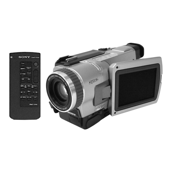
Photo : DCR-TRV530
RMT-814
For MECHANISM ADJUSTMENT, refer to the "8mm
Video MECHANICAL ADJUSTMENT MANUAL
M2000 MECHANISM " (9-929-861-11).
SPECIFICATIONS
DIGITAL VIDEO CAMERA RECORDER
RMT-814
US Model
Canadian Model
E Model
Hong Kong Model
Korea Model
DCR-TRV230/TRV330/TRV530
Tourist Model
DCR-TRV330/TRV530
Argentina Model
DCR-TRV230/TRV530
Brazilian Model
DCR-TRV330
M2000 MECHANISM
IX
— Continued on next page —
Advertisement
Table of Contents

Related Manuals for Sony DCR-TRV230


Summary of Contents for Sony DCR-TRV230
- Page 1 DCR-TRV230/TRV330/TRV530 RMT-814 SERVICE MANUAL SERVICE MANUAL US Model Canadian Model E Model Hong Kong Model Ver 1.2 2005. 06 Korea Model DCR-TRV230/TRV330/TRV530 Tourist Model DCR-TRV330/TRV530 Argentina Model DCR-TRV230/TRV530 Brazilian Model DCR-TRV330 Photo : DCR-TRV530 RMT-814 M2000 MECHANISM For MECHANISM ADJUSTMENT, refer to the “8mm Video MECHANICAL ADJUSTMENT MANUAL M2000 MECHANISM ”...
- Page 2 MARK 0 ON THE SCHEMATIC DIAGRAMS AND IN THE PARTS CRITIQUES POUR LA SÉCURITÉ DE FONCTIONNEMENT. NE LIST ARE CRITICAL TO SAFE OPERATION. REPLACE THESE REMPLACER CES COMPOSANTS QUE PAR DES PIÈSES SONY COMPONENTS WITH SONY PARTS WHOSE PART NUMBERS DONT LES NUMÉROS SONT DONNÉS DANS CE MANUEL OU APPEAR AS SHOWN IN THIS MANUAL OR IN SUPPLEMENTS DANS LES SUPPÉMENTS PUBLIÉS PAR SONY.
- Page 3 Table for difference of function Model DCR-TRV230 DCR-TRV330 DCR-TRV530 Remark US,CND,E,HK,KR, US,CND,E,HK,KR, US,CND,E,HK,KR, Destination JE,BR JE,AR 2.5 inch size 3.5 inch pixel 123K TYPE SH type TYPE SO a: with PC-082 board Memory stick a (P) a (P): Supports printer...
- Page 4 “Memory Stick” operations (DCR-TRV330/TRV530 only) 4-2. PRINTED WIRING BOARDS AND Using “Memory Stick” –introduction ·································· 1-21 SCHEMATIC DIAGRAMS ············································ 4-8 Recording still images on “Memory Stick”s • CD-292 (CCD IMAGER) –Memory Photo recording ················································ 1-22 PRINTED WIRING BOARD (DCR-TRV230/TRV330) ································ 4-9 — 4 —...
- Page 5 CONTROL, LASER LINK, DRUM CAPSTAN DRIVE, • CF-079/080 (EVF DRIVER)(2/2) AUDIO PROCESS, MIC, DC/DC CONVERTER) SCHEMATIC DIAGRAM ···························· 4-77 PRINTED WIRING BOARD ······················· 4-11 • SI-028 (DCR-TRV230/TRV330), SI-029 (DCR-TRV530) • VC-254 (CAMERA PROCESS)(1/18) (STEADY SHOT, REMOTE COMMANDER SCHEMATIC DIAGRAM ···························· 4-15 RECEIVER, LASER LINK) •...
- Page 6 PSIG Gray Adjustment (PD-139 board)(DCR-TRV530) · 5-30 (VC-254 board) ····························································· 5-56 RGB AMP Adjustment (PD-138 board) Hi8/Standard8 AFM 1.7 MHz Deviation Adjustment (DCR-TRV230/TRV330) ·············································· 5-31 (VC-254 board) ····························································· 5-56 RGB AMP Adjustment (PD-139 board)(DCR-TRV530) · 5-31 Digital8 Playback Level Check ····································· 5-56 Black Limit Adjustment (PD-139 board)(DCR-TRV530) ··...
- Page 7 Record of Use check ······················································ 5-64 Record of Self-diagnosis check ····································· 5-65 REPAIR PARTS LIST 6-1. EXPLODED VIEWS ······················································ 6-1 6-1-1. OVERALL SECTION ····················································· 6-1 6-1-2. CABINET (L) SECTION-1 ············································ 6-2 6-1-3. CABINET (L) SECTION-2 ············································ 6-3 6-1-4. CABINET (R) SECTION (2.5 INCH LCD MODEL) (TRV230/TRV330) ··························································...
-
Page 8: Service Note
SERVICE NOTE POWER SUPPLY DURING REPAIRS In this unit, about 10 seconds after power is supplied (8.4V) to the battery terminal using the service power code (J-6082-223-A), the power is shut off so that the unit cannot operate. These following two methods are available to prevent this. Take note of which to use during repairs. Method 1. -
Page 9: Service Mode Display
SELF-DIAGNOSIS FUNCTION Self-diagnosis Function Self-diagnosis Display When problems occur while the unit is operating, the self-diagnosis When problems occur while the unit is operating, the counter of the function starts working, and displays on the viewfinder or Display viewfinder or Display window shows a 4-digit display consisting window what to do. - Page 10 Self-diagnosis Code Table Self-diagnosis Code Block Detailed Symptom/State Correction Function Code Non-standard battery is used. Use the InfoLITHIUM battery. Condensation. Remove the cassette, and insert it again after one hour. Video head is dirty. Clean with the optional cleaning cassette. LOAD direction.
- Page 11 Self-diagnosis Code Block Detailed Symptom/State Correction Function Code Inspect the lens block focus reset sensor (Pin qd of CN1551 of Difficult to adjust focus VC-254 board) when focusing is performed when the control dial (Cannot initialize focus.) is rotated in the focus manual mode and the focus motor drive circuit (IC1553 of VC-254 board) when the focusing is not performed.
- Page 12 DCR-TRV230/TRV330/TRV530 SECTION 1 This section is extracted from GENERAL instruction manual.
- Page 21 1-10...
- Page 22 1-11...
- Page 23 1-12...
- Page 24 1-13...
- Page 25 1-14...
- Page 26 1-15...
- Page 27 1-16...
- Page 28 1-17...
- Page 29 1-18...
- Page 30 1-19...
- Page 31 1-20...
- Page 32 1-21...
- Page 33 1-22...
- Page 34 1-23...
- Page 35 1-24...
- Page 36 1-25...
- Page 37 1-26...
- Page 38 1-27...
- Page 39 1-28...
- Page 40 1-29...
- Page 41 1-30...
- Page 42 1-31...
- Page 43 1-32...
- Page 44 1-33...
- Page 45 1-34...
- Page 46 1-35...
- Page 47 1-36...
- Page 48 1-37E...
- Page 49 DCR-TRV230/TRV330/TRV530 SECTION 2 DISASSEMBLY The following flow chart shows the disassembly procedure. PD-138 board service position 2-1. LCD unit, PD-138 board (TRV230/TRV330) PD-139 board service position 2-2. LCD unit, PD-139 board (TRV530) 2-3. Front panel section, SI-028/029 board SI-028/029 board service position 2-4.
- Page 50 NOTE: Follow the disassembly procedure in the numerical order given. 2-1. LCD UNIT, PD-138 BOARD (TRV230/TRV330) 3 Two claws REMOVING THE BACK LIGHT P cabinet C (2) screws (M2 × 4) (H) Remove the indication LCD block assembly, back light in the direction of the arrow B . 5 Screw (M1.7 ×...
- Page 51 2-2. LCD UNIT, PD-139 BOARD (TRV530) REMOVING THE BACK LIGHT P cabinet C (3) assembly screws Remove the indication LCD block assembly, Two screws (M2 × 4) (H) back light in the direction of the arrow B . (M1.7 × 2.5), p 5 Screw (M1.7 ×...
-
Page 52: Trv230/Trv330) ··························································
2-3. FRONT PANEL SECTION, SI-028/029 BOARD Push the eject knob in the direction of the arrow A , and open the cassette lid. screws (M2 × 4) (H) REMOVING THE SI-028/029 BOARD Remove the FP-273 board in the 1 Cushion (SI) direction of the arrow B . - Page 53 2-4. CABINET (R) SECTION 1 MI screw screws (M2 × 4) (H) Three claws (M2 × 4) (H) screws (M2 × 4) (H) 3 Cabinet (upper) 6 MI screw (M2 × 4) (H) Harness (VP-076) (20P) Two tapping screws (M1.7 × 5) Flexible flat cable (FFC-001) (45P) screws...
-
Page 54: Trv530) ·········································································
2-6. CF-080 BOARD (TRV530) REMOVING THE CF-080 BOARD Tape (A) Cabinet (R) block Harness Tape (A) assembly (VP-076) CF electrostatic sheet (4) Cabinet (R) block CF electrostatic assembly sheet (3) Control switch block (SE-1380) Tapping screw (B2 × 5) Two tapping screws (B2 ×... - Page 55 2-7. EVF SECTION, LB-068/070 BOARD PRECAUTION WHEN ATTACHING 3 B label FP-268 FLEXIBLE BOARD 1 FP-268 flexible board (20P) EVF section FP-268 flexible board Flexible Three tapping guide screws (B2 × 5) EVF section Fix the FP-268 flexible board to both the EVF section, flexible guide with the both-sided adhesive tape.
-
Page 56: Trv230/Trv330) ··························································
2-8. LENS SECTION, CD-292/315 BOARD REMOVING THE IRIS FLEXIBLE ASSEMBLY 3 FP-265 flexible board (16P) Two tapping screws (B1.7 × 3.5), head 2 Tape (A) Tapping screw (M1.7 × 5) 3 Remove the eight 1 Electrostatic solderings sheet T Two tapping screws (M1.7 ×... - Page 57 2-9. PC-082 BOARD (TRV330/TRV530) Three screws (M1.7 × 2.5), p FP-274 flexible board (12P) - 2 5 Ferrite bead a r d REMOVING THE FP-274 FLEXIBLE BOARD - 0 8 MS holder a r d Memory stick connector FP-271 board (6P) 4 Remove the two solderings...
- Page 58 2-10.BATTERY PANEL SECTION, BATTERY TERMINAL BOARD 3 MI screw 4 Claw Remove the battery panel section 2 MI screw (M2 × 4) (H) (M2 × 4) (H) in the direction of the arrow A . Tapping screw (M1.7 × 5) - 2 5 a r d 6 MI...
- Page 59 2-12.CABINET (L) SECTION, MECHANISM DECK-1 Four dowels Screw (M1.7 × 2.5), p REMOVING THE CS FRAME ASSEMBLY Cabinet (L) section, CS frame assembly Cabinet (L) 2 Two MI screws (M2 × 4) (H) assembly 1 MI screw (M2 × 4) (H) - 2 5 a r d Screw...
- Page 60 2-13.VC-254 BOARD Remove the VC-254 board Remove the flexible boards in the direction of the arrow H . Screw (M1.7 × 2.5), p 3 VC sheet - 2 5 a r d FP-264 flexible Two screws (M1.7 × 2.5), p board (15, 20P) (TRV330/TRV530) FP-272 board...
- Page 61 [CONNECTION DIAGRAM FOR SERVICE POSITION (Mainly for voltage measurement and check)] (VC-254, FU-150/154, CD-292/315, SI-028/029, PC-082, CF-079/080 BOARDS MECHANISM DECK-2) Note: Operate the VTR using the adjustment remote commander (with the HOLD switch set in the OFF position) Battery panel section FU-150 board (TRV230/TRV330), AC POWER...
-
Page 62: Hinge Section
2-15.HINGE SECTION [TRV230/TRV330 MODEL] Four tapping screws 0 For removing the LCD unit (B2 × 5) (See page 2-2) claws Harness Hinge cover (140) (VP-076) (6P) assembly 7 FP-282 board (6P) REMOVING THE HINGE ASSEMBLY Control switch block (SE-1380) Tapping screw (B2 ×... - Page 63 2-16.CIRCUIT BOARDS LOCATION LB-068 (TRV230/TRV330) LB-070 (TRV530) (EVF BACK LIGHT) CF-079 (TRV230/TRV330) CF-080 (TRV530) CD-292 (TRV230/TRV330) (USER FUNCTION, EVF DRIVE) CD-315 (TRV530) (CCD IMAGER) PD-138 (TRV230/TRV330) PD-139 (TRV530) RGB DRIVE, TIMING GENERATOR, LCD DRIVE, BACK LIGHT DRIVE PC-082 (TRV330/TRV530) FU-150 (TRV230/TRV330) DIGITAL STILL CONTROL, FU-154 (TRV530) DS STILL PROCESS...
- Page 64 2-17.FLEXIBLE BOARDS LOCATION The flexible boards contained in the mechanism deck are not shown. FP-268 FP-264 FP-274 FP-265 (TRV330/TRV530) FP-266 CONTROL SWITCH BLOCK (SS-1380) CONTROL SWITCH BLOCK (SE-1380) IRIS FLEXIBLE ASSEMBLY FFC-001 2-16E...
- Page 65 DCR-TRV230/TRV330/TRV530 SECTION 3 BLOCK DIAGRAMS 3-1. OVERALL BLOCK DIAGRAM (1/5) ( ) : Page No. shown in ( ) indicates the page to refer on the schematic diagram. CN1108(1/4) FOR ADJUSTMENTS CD-292 BOARD (TRV230/TRV330) VC-254 BOARD(1/4) AFC F0 CD-315 BOARD...
- Page 66 DCR-TRV230/TRV330/TRV530 3-2. OVERALL BLOCK DIAGRAM (2/5) ( ) : Page No. shown in ( ) indicates the page to refer on the schematic diagram. (TRV530) PC-082 BOARD (4-64) CN1901 CN1901 SPCK IC1901 AFCK Y0-Y7 (L-PLATZ) DS STILL PROCESS Y0-Y7 C0-C3...
- Page 67 DCR-TRV230/TRV330/TRV530 3-3. OVERALL BLOCK DIAGRAM (3/5) ( ) : Page No. shown in ( ) indicates the page to refer on the schematic diagram. CN202 DV IN/OUT VC-254 BOARD(2/4) (4-21) X3301 IC3301 24.576MHz (CAIN) CN1114 (4-23) TPA+,- DV SIGNAL IC3303...
- Page 68 DCR-TRV230/TRV330/TRV530 3-4. OVERALL BLOCK DIAGRAM (4/5) ( ) : Page No. shown in ( ) indicates the page to refer on the schematic diagram. M2000 MECHA DECK VC-254 BOARD(3/4) (4-42) (SEE PAGE 4-52) (4-39) (4-42) M901 IC4401 IC1301 CN4402 Q1306...
- Page 69 DCR-TRV230/TRV330/TRV530 3-5. OVERALL BLOCK DIAGRAM (5/5) ( ) : Page No. shown in ( ) indicates the page to refer on the schematic diagram. CF-079 BOARD(2/2) VC-254 BOARD(4/4) (4-34) CN1101 (TRV230/TRV330) IC4803 LANC SIG INTELLIGENT CF-080 BOARD(2/2) HI CONTROL SHOE/PRT UNREG...
- Page 70 DCR-TRV230/TRV330/TRV530 3-6. POWER BLOCK DIAGRAM (1/3) ( ) : Page No. shown in ( ) indicates the page to refer on the schematic diagram. (SEE PAGE 4-101) (TRV330/TRV530) CN1113 Q405,408-412 F405 PRT HEAD UNREG FU-150 BOARD(1/2) VC-254 BOARD(1/2) INTELLIGENT (TRV230/TRV330)
- Page 71 DCR-TRV230/TRV330/TRV530 3-7. POWER BLOCK DIAGRAM (2/3) ( ) : Page No. shown in ( ) indicates the page to refer on the schematic diagram. CONTROL SWITCH BLOCK FU-150 BOARD FU-154 BOARD VC-254 BOARD(2/2) (SS-1380) (2/2) (2/2) (SEE PAGE 4-101) (TRV230/TRV330)
- Page 72 DCR-TRV230/TRV330/TRV530 3-8. POWER BLOCK DIAGRAM (3/3) ( ) : Page No. shown in ( ) indicates the page to refer on the schematic diagram. PD-138/139 (4-62) PD-139 BOARD LCD901 PC-082 BOARD (TRV530) BOARD D5503 IC1157 Q5505,5506 PANEL 13.3V FB5504 UNIT...
-
Page 73: Dcr-Trv230/Trv330) ································
DCR-TRV230/TRV330/TRV530 SECTION 4 PRINTED WIRING BOARDS AND SCHEMATIC DIAGRAMS 4-1. FRAME SCHEMATIC DIAGRAM (1/3) CD-292 BOARD (DCR-TRV230/TRV330) CD-315 BOARD (DCR-TRV530) LENS UNIT FP-272 J201 IMAGER FLEXIBLE LANC CN202 NTPA DV IN/OUT NTPB FP-265 FLEXIBLE VC-254 BOARD(1/3) 1/18 CAMERA PROCESS 10/18 MODE CONTROL... - Page 74 DCR-TRV230/TRV330/TRV530 FRAME SCHEMATIC DIAGRAM (2/3) CONTROL SWITCH BLOCK(SE-1380) FP-275 FLEXIBLE FP-282 S405/ D401 S103/S102 FLEXIBLE S401-404,S406-409 SEL/PUSH EXEC S101 PANEL OPEN/CLOSE STOP ,SUPER NIGHT SHOT, S501 PAUSE, FOCUS EXPOSURE S910 REC, REW, PLAY AUIO→MANUAL SUPER LASER LINK LCD 903 SP901...
- Page 75 DCR-TRV230/TRV330/TRV530 FRAME SCHEMATIC DIAGRAM (3/3) DCR-TRV330/TRV530 PC-082 BOARD 1/3 DIGITAL STILL CONTROL1 REG_GND REG_GND REG_GND REG_GND 2/3 DIGITAL STILL CONTROL2 REG_GND REG_GND REG_GND REG_GND 3/3 DS STILL PROCESS REG_GND DS_MAD REG_GND DS_MAD MS_LED XDS_FLASH_RST MS_LED XDS_FLASH_RST FP-271 RTS/IR_L TXD/IR_R FLEXIBLE...
- Page 76 DCR-TRV230/TRV330/TRV530 DCR-TRV230/TRV330/TRV530 4-2. PRINTED WIRING BOARDS AND SCHEMATIC DIAGRAMS THIS NOTE IS COMMON FOR WIRING BOARDS AND SCHEMATIC DIAGRAMS (In addition to this, the necessary note is printed in each block) (For printed wiring boards) (Measuring conditions voltage and waveform) •...
- Page 77 DCR-TRV230/TRV330/TRV530 CD-292 (CCD IMAGER) PRINTED WIRING BOARD (DCR-TRV230/TRV330) CD-315 (CCD IMAGER) PRINTED WIRING BOARD (DCR-TRV530) For Schematic Diagram — Ref. No. CD-292, CD-315 Boards; 10,000 Series — • Refer to page 4-103 for waveforms. CD-292 BOARD (DCR-TRV230/TRV330) CD-315 BOARD (DCR-TRV530) CCD IMAGER -REF.NO.:10000 SERIES-...
- Page 78 DCR-TRV230/TRV330/TRV530 VC-254 (CAMERA/STD8/Hi8/PB PROCESS, DV SIGNAL, PB RF AMP, VIDEO IN/OUT, AD CONVERTER, MODE/CAMERA/MECHA CONTROL, LASER LINK, DRUM CAPSTAN DRIVE, AUDIO PROCESS, MIC, DC/DC CONVERTER) PRINTED WIRING BOARD — Ref. No. VC-254 Board; 10,000 Series — CAMERA/PB PROCESS, PB/REC AMP, ANALOG/DIGITAL PROCESS, VIDEO/AUDIO PROCESS, POWER SUPPLY...
- Page 79 DCR-TRV230/TRV330/TRV530 For printed wiring board • Refer to pages 4-107 to 109 for parts location. • VC-254 board consists of multiple layers. However, only the sides (layers) A and B are shown. • Chip parts Transistor Diode There are a few cases that the part printed on this diagram isn’t mounted in this model.
- Page 80 DCR-TRV230/TRV330/TRV530 For Schematic Diagram • Refer to page 4-11 for printed wiring board. • Refer to page 4-103 for waveforms. VC-254 BOARD(1/18) CAM_15V REG_GND CAMERA PROCESS(CAM BLOCK) A_2.8V TO(18/18) -REF.NO.: 10000 SERIES- A_4.75V XX MARK:NO MOUNT CAM_-7.5V D_2.8V NO MARK:REC/PB MODE...
- Page 81 DCR-TRV230/TRV330/TRV530 For Schematic Diagram • Refer to page 4-11 for printed wiring board. • Refer to page 4-103 for waveforms. VC-254 BOARD(2/18) CAMERA PROCESS,HI8/STD8 PB PROCESS L2209 -REF.NO.:10000 SERIES- 10uH XX MARK:NO MOUNT FB2205 NO MARK:REC/PB MODE FB2204 R :REC MODE D_2.8V...
- Page 82 DCR-TRV230/TRV330/TRV530 For Schematic Diagram • Refer to page 4-11 for printed wiring board. VC-254 BOARD(3/18) IRIS/FOCUS/ZOOM DRIVE(LD BLOCK) -REF.NO.:10000 SERIES- R1567 2200 HALL_REF R1568 XX MARK:NO MOUNT C1562 0.22u HALL_GAIN R1572 TO(12/18) NO MARK:REC/PB MODE R1570 R :REC MODE R1565...
- Page 83 DCR-TRV230/TRV330/TRV530 For Schematic Diagram • Refer to page 4-11 for printed wiring board. • Refer to page 4-103 for waveforms. VC-254 BOARD(4/18) NO MARK:REC/PB MODE R :REC MODE DV SIGNAL PROCESS(JC BLOCK) P :PB MODE -REF.NO.:10000 SERIES- XX MARK:NO MOUNT TO(6/18) RF_1.9V...
-
Page 84: Dcr-Trv230/Trv330) ······························
DCR-TRV230/TRV330/TRV530 For Schematic Diagram • Refer to page 4-11 for VC-254 printed wiring board. • Refer to page 4-53 for printed wiring board of FP-272 flexible. C3332 L3307 0.01u VC-254 BOARD(5/18) 10uH D_2.8V DV SIGNAL PROCESS(JC-2 BLOCK) C3331 FB3304 TO(18/18) -REF.NO.:10000 SERIES-... - Page 85 DCR-TRV230/TRV330/TRV530 For Schematic Diagram • Refer to page 4-11 for printed wiring board. • Refer to page 4-103 for waveforms. VC-254 BOARD(6/18) DIGITAL8 PB RF AMP(RF(D) BLOCK) -REF.NO.:10000 SERIES- XX MARK:NO MOUNT NO MARK:REC/PB MODE R :REC MODE P :PB MODE RP_4.75V...
- Page 86 DCR-TRV230/TRV330/TRV530 For Schematic Diagram • Refer to page 4-11 for printed wiring board. • Refer to page 4-104 for waveforms. VC-254 BOARD(7/18) NO MARK:REC/PB MODE R :REC MODE VIDEO IN/OUT P :PB MODE A_4.75V -REF.NO.:10000 SERIES- XX MARK:NO MOUNT D_2.8V...
- Page 87 DCR-TRV230/TRV330/TRV530 For Schematic Diagram • Refer to page 4-11 for printed wiring board. VC-254 BOARD(8/18) NO MARK:REC/PB MODE R :REC MODE VIDEO A/D CONV. P :PB MODE TO(10/18,11/18 -REF.NO.:10000 SERIES- 13/18,17/18(CN1104)) HI_SI XX MARK:NO MOUNT XCS_ALIGN TO(10/18) L3602 FB3601 10uH...
- Page 88 DCR-TRV230/TRV330/TRV530 For Schematic Diagram • Refer to page 4-11 for printed wiring board. VC-254 BOARD(9/18) HI8/STD8 PB RF AMP(RF(8)BLOCK) REG_GND -REF.NO.:10000 SERIES- RP_4.75V TO(18/18) XX MARK:NO MOUNT A_2.8V NO MARK:REC/PB MODE DV_PB_RF TO(6/18) R :REC MODE P :PB MODE L3201...
- Page 89 DCR-TRV230/TRV330/TRV530 For Schematic Diagram • Refer to page 4-11 for printed wiring board. • Refer to page 4-104 for waveforms. VC-254 BOARD(10/18) MODE CONTROL (HI BLOCK) Q4801 -REF.NO.:10000 SERIES- 2SC4738F-Y/GR(TPL3) XX MARK:NO MOUNT BUFFER HI_XRESET MELODY_ENV Q4806 RN2102F(TPL3) R4801 XLANC_ON...
- Page 90 DCR-TRV230/TRV330/TRV530 For Schematic Diagram • Refer to page 4-11 for printed wiring board. • Refer to page 4-104 for waveform. TO(6/18,15/18, TO(1/18, TO(17/18 TO(17/18 TO(12/18) TO(6/18) TO(9/18) TO(5/18) TO(2/18) TO(1/18) TO(3/18) 17/18(CN1108)) 2/18) (CN1113)) (CN1116)) VC-254 BOARD(11/18) CAMERA CONTROL,HI8/STD8 MECHA CONTROL,...
- Page 91 DCR-TRV230/TRV330/TRV530 For Schematic Diagram • Refer to page 4-11 for printed wiring board. • Refer to page 4-104 for waveforms. VC-254 BOARD(12/18) EVR, LASER LINK(ER,IR BLOCK) NO MARK:REC/PB MODE R :REC MODE -REF.NO.:10000 SERIES- P :PB MODE XX MARK:NO MOUNT...
- Page 92 DCR-TRV230/TRV330/TRV530 For Schematic Diagram • Refer to page 4-11 for printed wiring board. • Refer to page 4-104 for waveforms. VC-254 BOARD(13/18) DIGITAL8 MECHA CONTROL(MC BLOCK) REG_GND TO(18/18) -REF.NO.:10000 SERIES- D_2.8V FB4501 XX MARK:NO MOUNT NO MARK:REC/PB MODE R :REC MODE...
- Page 93 DCR-TRV230/TRV330/TRV530 For Schematic Diagram • Refer to page 4-11 for printed wiring board. • Refer to page 4-104 for waveforms. VC-254 BOARD(14/18) DRUM/CAPSTAN DRIVE(MD BLOCK) CAP_VS VTR_UNREG -REF.NO.:10000 SERIES- DRUM_VS XX MARK:NO MOUNT MT_5V NO MARK:REC/PB MODE MT_GND R :REC MODE...
- Page 94 DCR-TRV230/TRV330/TRV530 For Schematic Diagram • Refer to page 4-11 for printed wiring board. • Refer to page 4-104 for waveform. VC-254 BOARD(15/18) NO MARK:REC/PB MODE AUDIO PROCESS(AU BLOCK) R :REC MODE P :PB MODE -REF.NO.:10000 SERIES- XX MARK:NO MOUNT AU_4.75V AU_2.8V...
- Page 95 DCR-TRV230/TRV330/TRV530 For Schematic Diagram • Refer to page 4-11 for printed wiring board. VC-254 BOARD(16/18) MIC AMP(MA BLOCK) -REF.NO.:10000 SERIES- REG_GND TO(18/18) XX MARK:NO MOUNT AU_2.8V NO MARK:REC/PB MODE R :REC MODE SHOE_MIC_L P :PB MODE C5832 R5801 R5823 0.022u...
- Page 96 DCR-TRV230/TRV330/TRV530 For Schematic Diagram • Refer to page 4-11 for printed wiring board. VC-254 BOARD(17/18) TO PC-082 BOARD(3/3) CN1901 CONNECTOR(CN BLOCK) (DCR-TRV330/TRV530) (SEE PAGE 4-63) -REF.NO.:10000 SERIES- XX MARK:NO MOUNT NO MARK:REC/PB MODE R :REC MODE P :PB MODE C1104 D1102,1105 0.1u...
- Page 97 DCR-TRV230/TRV330/TRV530 For Schematic Diagram • Refer to page 4-11 for printed wiring board. • Refer to page 4-104 for waveforms. VC-254 BOARD(18/18) DC/DC CONV.(DD BLOCK) -REF.NO.:10000 SERIES- CAM_15V NO MARK:REC/PB MODE XX MARK:NO MOUNT R :REC MODE CAM_-7.5V A_4.75V P :PB MODE A_4.75V...
- Page 98 DCR-TRV230/TRV330/TRV530 LS-057 (S/T REEL SENSOR), FP-228 (DEW SENSOR), FP-229 (MODE SWITCH), FP-300 (TAPE TOP), FP-302 (TAPE END), FP-301 (TAPE LED) FLEXIBLE BOARDS FP-302 FP-300 FLEXIBLE (COMPONENT SIDE) LS-057 BOARD FP-300 FLEXIBLE FLEXIBLE Q002 Q001 TAPE END TAPE TOP FP-301 TAPE TOP (C)
- Page 99 DCR-TRV230/TRV330/TRV530 FP-270 (S VIDEO, AUDIO/VIDEO), FP-272 (LANC, DV IN/OUT) FLEXIBLE BOARDS — Ref. No. FP-270, FP-272 Flexible Boards; 30,000 Series — • Refer to page 4-27 for schematic diagram. • Refer to page 4-24 for schematic diagram. For printed wiring boards PC-082 (TRV330/TRV530) •...
- Page 100 DCR-TRV230/TRV330/TRV530 PC-082 (DIGITAL STILL CONTROL, DS STILL PROCESS) PRINTED WIRING BOARD — Ref. No. PC-082 Board; 20,000 Series — For printed wiring boards • Refer to page 4-109 for parts location. • PC-082 board consists of multiple layers. However, only the sides (layers) A and B are shown.
- Page 101 DCR-TRV230/TRV330/TRV530 DIGITAL STILL CONTROL, DS STILL PROCESS 4-57 PC-082...
- Page 102 DCR-TRV230/TRV330/TRV530 For Schematic Diagram • Refer to page 4-55 for PC-082 printed wiring board. • Refer to page 4-105 for waveform. PC-082 BOARD(1/3) (DCR-TRV330/TRV530) DIGITAL STILL CONTROL1 -REF.NO.:20000 SERIES- XX MARK:NO MOUNT C1153 X1151 NO MARK:REC/PB MODE 48MHz R :REC MODE...
- Page 103 DCR-TRV230/TRV330/TRV530 For Schematic Diagram • Refer to page 4-55 for PC-082 printed wiring board. • Refer to page 4-65 for printed wiring board of FP-271 flexible. PC-082 BOARD(2/3) (DCR-TRV330/TRV530) DIGITAL STILL CONTROL2 -REF.NO.:20000 SERIES- XX MARK:NO MOUNT NO MARK:REC/PB MODE...
- Page 104 DCR-TRV230/TRV330/TRV530 For Schematic Diagram • Refer to page 4-55 for printed wiring board. PC-082 BOARD(3/3) (DCR-TRV330/TRV530) CN1901 100P B_TO_B TO(1/3) DS STILL PROCESS REG_GND -REF.NO.:20000 SERIES- REG_GND VFI_Y0 XX MARK:NO MOUNT VFI_Y0 VFI_OE VFI_HD VFI_OE VFI_HD VFI_VD NO MARK:REC/PB MODE...
- Page 105 DCR-TRV230/TRV330/TRV530 FP-271 (USB), FP-282 (FOCUS), FP-275 (SWITCH) FLEXIBLE BOARDS — Ref. No. FP-271, FP-282, FP-275 Flexible Boards; 30,000 Series — • Refer to page 4-62 for schematic diagram. • Refer to page 4-76 for schematic diagram. For printed wiring boards •...
- Page 106 DCR-TRV230/TRV330/TRV530 CF-079 (USER FUNCTION, EVF DRIVE) PRINTED WIRING BOARD (DCR-TRV230/TRV330) — Ref. No. CF-079 Board; 1,000 Series — For printed wiring board • Refer to page 4-109 for parts location. • CF-079 board consists of multiple layers. However, only the sides (layers) A and B are shown.
- Page 107 DCR-TRV230/TRV330/TRV530 USER FUNCTION, EVF DRIVE 4-69 4-70 CF-079...
- Page 108 DCR-TRV230/TRV330/TRV530 CF-080 (USER FUNCTION, EVF DRIVE) PRINTED WIRING BOARD (DCR-TRV530) — Ref. No. CF-080 Board; 1,000 Series — For printed wiring board • Refer to page 4-110 for parts location. • CF-080 board consists of multiple layers. However, only the sides (layers) A and B are shown.
- Page 109 DCR-TRV230/TRV330/TRV530 USER FUNCTION, EVF DRIVE 4-73 4-74 CF-080...
- Page 110 DCR-TRV230/TRV330/TRV530 For Schematic Diagram • Refer to page 4-67 (CF-079), 4-71 (CF-080) for printed wiring board. • Refer to page 4-65 for printed wiring boards of FP-282, FP-275 flexible. (DCR-TRV230/TRV330) CF-079 BOARD(1/2) FP-275 FLEXIBLE CF-080 BOARD(1/2) (DCR-TRV530) VCR SWITCH CL001 USER FUNCTION -REF.NO.:1000 SERIES-...
- Page 111 DCR-TRV230/TRV330/TRV530 For Schematic Diagram • Refer to page 4-67 (CF-079), 4-71 (CF-080) for printed wiring board. • Refer to page 4-105 for waveforms. CF-079 BOARD(2/2) (DCR-TRV230/TRV330) CF-080 BOARD(2/2) (DCR-TRV530) EVF DRIVE FB202 -REF.NO.:1000 SERIES- C214 XX MARK:NO MOUNT 3.3u NO MARK:REC/PB MODE...
-
Page 112: Dcr-Trv230/Trv330) ······························
DCR-TRV230/TRV330/TRV530 SI-028 (DCR-TRV230/TRV330), SI-029 (DCR-TRV530) (STEADY SHOT, REMOTE COMMANDER RECEIVER, LASER LINK) PRINTED WIRING BOARDS — Ref. No. SI-028, SI-029 Boards; 1,000 Series — Suffix No.-12 Suffix No.-12, -13 For printed wiring boards SI-028 (TRV230/TRV330) • Refer to page 4-110 for parts location. -
Page 113: Dcr-Trv230/Trv330) ······························
DCR-TRV230/TRV330/TRV530 FP-273 (MIC, HEADPHONES) FLEXIBLE BOARD (DCR-TRV530) For Schematic Diagram — Ref. No. FP-273 Flexible Board; 30,000 Series — • Refer to page 4-79 for printed wiring board. SI-028 BOARD (DCR-TRV230/TRV330) NO MARK:REC/PB MODE SI-029 BOARD (DCR-TRV530) R :REC MODE... - Page 114 DCR-TRV230/TRV330/TRV530 LB-068 (EVF, BACK LIGHT) PRINTED WIRING BOARD (DCR-TRV230/TRV330) LB-070 (EVF, BACK LIGHT) PRINTED WIRING BOARD (DCR-TRV530) — Ref. No. LB-068, LB-070 Boards; 1,000 Series — For printed wiring boards • Refer to page 4-110 for parts location. • LB-068, LB-070 boards consists of multiple layers.
- Page 115 DCR-TRV230/TRV330/TRV530 FP-283 (PANEL REVERSE) FLEXIBLE BOARD For Schematic Diagram — Ref. No. FP-283 Flexible Board; 30,000 Series — • Refer to page 4-83 for printed wiring board. • Refer to page 4-89 for schematic diagram. (DCR-TRV230/TRV330) LB-068 BOARD LB-070 BOARD...
- Page 116 DCR-TRV230/TRV330/TRV530 PD-138 (RGB DRIVE, TIMING GENERATOR, LCD DRIVE, BACK LIGHT DRIVE) PRINTED WIRING BOARD (DCR-TRV230/TRV330) — Ref. No. PD-138 Board; 20,000 Series — For printed wiring board • Refer to page 4-110 for parts location. • PD-138 board consists of multiple layers. However, only the sides (layers) A and B are shown.
- Page 117 DCR-TRV230/TRV330/TRV530 For Schematic Diagram • Refer to page 4-87 for PD-138 printed wiring board. • Refer to page 4-86 for printed wiring board of FP-283 flexible. • Refer to page 4-105 for waveforms. PD-138 BOARD(1/2) (DCR-TRV230/TRV330) FB5503 RGB DRIVE,TIMING GENERATOR 1608 -REF.NO.:20000 SERIES-...
- Page 118 DCR-TRV230/TRV330/TRV530 For Schematic Diagram • Refer to page 4-87 for printed wiring board. • Refer to page 4-106 for waveform. FP-276 PD-138 BOARD(2/2) (DCR-TRV230/TRV330) CN5705 FLEXIBLE LCD DRIVE,BACKLIGHT DRIVE COM1 COM1 COM2 -REF.NO.:20000 SERIES- COM2 SEG3 XX MARK:NO MOUNT SEG3...
- Page 119 DCR-TRV230/TRV330/TRV530 PD-139 (RGB DRIVE, TIMING GENERATOR, LCD DRIVE, BACK LIGHT DRIVE) PRINTED WIRING BOARD (DCR-TRV530) — Ref. No. PD-139 Board; 20,000 Series — For printed wiring board • Refer to page 4-111 for parts location. • PD-139 board consists of multiple layers. However, only the sides (layers) A and B are shown.
- Page 120 DCR-TRV230/TRV330/TRV530 For Schematic Diagram • Refer to page 4-93 for PD-139 printed wiring board. • Refer to page 4-86 for printed wiring board of FP-283 flexible. • Refer to page 4-106 for waveforms. PD-139 BOARD(1/2) (DCR-TRV530) L5504 RGB DRIVE,TIMING GENERATOR 2520 -REF.NO.:20000 SERIES-...
- Page 121 DCR-TRV230/TRV330/TRV530 For Schematic Diagram • Refer to page 4-93 for printed wiring board. • Refer to page 4-106 for waveform. PD-139 BOARD(2/2) (DCR-TRV530) LCD DRIVE,BACKLIGHT DRIVE FP-277 -REF.NO.:20000 SERIES- FLEXIBLE CN5705 XX MARK:NO MOUNT COM1 COM1 COM2 NO MARK:REC/PB MODE...
- Page 122 DCR-TRV230/TRV330/TRV530 FU-150 (POWER SUPPLY) PRINTED WIRING BOARD (DCR-TRV230/TRV330) FU-154 (POWER SUPPLY) PRINTED WIRING BOARD (DCR-TRV530) — Ref. No. FU-150, FU-154 Boards; 1,000 Series — For printed wiring boards • Refer to page 4-111 for parts location. • FU-150, FU-154 boards consists of multiple layers.
- Page 123 DCR-TRV230/TRV330/TRV530 For Schematic Diagram • Refer to page 4-99 for printed wiring board. FU-150 BOARD (DCR-TRV230/TRV330) CN403 ZOOM_VR_AD ZOOM_VR_AD FU-154 BOARD (DCR-TRV530) BATT_SIG FAST_CHARGE POWER SUPPLY SHOE_ON -REF.NO.:1000 SERIES- BATT/XEXT_SW L401 XS/S_SW 4.7uH XX MARK:NO MOUNT F404 XS/S_SW 3225 1.4A...
- Page 124 DCR-TRV230/TRV330/TRV530 4-3. WAVEFORMS CD-292/315 VC-254 BOARD BOARD CAMERA REC IC1502 2 – qa IC2201 yj IC2201 <z., IC3301 <zc. IC4803 r; IC3701 7 IC3701 rk¢ IC501 1,2 CAMERA REC/PB CAMERA REC/PB CAMERA REC/PB CAMERA REC/PB CAMERA REC/PB LINE REC (S-C IN) S JACK IN 0.46Vp-p...
- Page 125 DCR-TRV230/TRV330/TRV530 PC-082 CF-079/080 PD-138 BOARD BOARD BOARD (1/2) REC/PB IC1155 <zcv IC5501 rk IC5502 wh IC201 w; 0.5Vp-p 3.6Vp-p 7.2Vp-p 3.0Vp-p 6 MHz 20.8 nsec IC5501 rj IC201 ws 0.5Vp-p 7.2Vp-p IC5501 rh IC201 wf 0.5Vp-p 7.2Vp-p IC5501 w; IC201 rk 3.0Vp-p...
- Page 126 DCR-TRV230/TRV330/TRV530 PD-139 PD-138/139 BOARD (1/2) BOARD (2/2) REC/PB IC5701 2 IC5501 w; IC5502 wh 3.0Vp-p 25.346 kHz 4.7Vp-p 8.0Vp-p 85 nsec IC5501 ws 8.0Vp-p IC5501 wf 8.0Vp-p IC5501 rk 600mVp-p IC5501 rj 600mVp-p IC5501 rh 600mVp-p IC5502 1 2.8Vp-p IC5502 rk 2.8Vp-p...
-
Page 127: Mounted Parts Location
DCR-TRV230/TRV330/TRV530 4-4. MOUNTED PARTS LOCATION CD-292/315 BOARD (SIDE A) VC-254 BOARD (SIDE A) C502 C1320 C3121 C4423 L1307 R1370 A-8 R3704 C-4 C503 C1328 C3122 C4424 L1308 R1519 F-4 R3705 C-4 C507 C1333 C3123 C4425 L1309 R1520 F-4 R3706 B-3... - Page 128 DCR-TRV230/TRV330/TRV530 VC-254 BOARD (SIDE B) C1101 E-16 C3117 G-14 C3918 B-18 C5740 C-16 IC1301 B-11 Q5718 A-16 R1574 D-16 R3371 C-11 R4820 B-15 C1102 F-16 C3119 G-14 C3919 A-18 C5741 C-16 IC1304 B-13 R1575 D-16 R3372 C-11 R4821 B-15 C1104...
- Page 129 DCR-TRV230/TRV330/TRV530 VC-254 BOARD (SIDE B) PC-082 BOARD (SIDE A) PC-082 BOARD (SIDE B) CF-079 BOARD (SIDE A) R5830 B-17 C1151 Q1153 C-3 C1164 R1177 B-8 BT101 IC201 R5831 B-17 C1152 Q1156 B-6 C1165 R1180 C-12 IC202 R5834 B-18 C1153 Q1157 D-4...
- Page 130 DCR-TRV230/TRV330/TRV530 CF-080 BOARD (SIDE A) SI-028/029 BOARD LB-068/070 BOARD PD-138 BOARD (SIDE A) (SIDE A) (SIDE A) BT101 IC201 C5501 Q5501 C-5 IC202 C5503 Q5502 A-3 C301 F301 C702 C101 IC203 C5504 Q5509 A-3 C304 C201 C5505 Q5510 B-3 C305...
- Page 131 DCR-TRV230/TRV330/TRV530 PD-139 BOARD (SIDE A) FU-150/154 BOARD (SIDE A) C5501 Q5505 A-3 C401 L401 C5503 Q5506 B-3 C402 C5504 Q5508 B-3 C403 LF401 C5505 Q5602 D-3 C404 C5506 Q5603 B-2 C405 Q401 C5507 C406 Q402 C5508 R5501 A-5 C407 Q403...
- Page 132 DCR-TRV230/TRV330/TRV530 SECTION 5 ADJUSTMENTS...
-
Page 133: Before Starting Adjustment
Before starting adjustment 1-1. Adjusting items when replacing main parts and boards. When replacing main parts, adjust the items indicated by in the following table. Replaced parts Block replacement Parts replacement Adjustment Adjustment Section Initialization of Initialization of C, D, 8 page data B,C,D,E,F,7,8 Initialization of B page data *2 page data... -
Page 134: Dcr-Trv230/Trv330) ······························
*4: DCR-TRV530 *5: CF-079 board (Part No. suffix: 12 or later) CF-080 board (Part No. suffix: 13 or later) Adjustment Adjustment Section Note: CD-292 board: DCR-TRV230/TRV330 CD-315 board: DCR-TRV530 CF-079 board: DCR-TRV230/TRV330 CF-080 board: DCR-TRV530 PD-138 board: DCR-TRV230/TRV330 PD-139 board: DCR-TRV530... -
Page 135: Preparations ·····································································
5-1. CAMERA SECTION ADJUSTMENT 1-1. PREPARATIONS BEFORE ADJUSTMENT (CAMERA SECTION) 1-1-1. List of Service Tools • Oscilloscope • Color monitor • Vectorscope • Regulated power supply • Digital voltmeter Ref. No. Name Parts Code Usage Auto white balance adjustment/check Filter for color temperature correction (C14) J-6080-058-A White balance adjustment/check ND filter 1.0... - Page 136 1-1-2. Preparations Note1: For details of how remove the cabinet and boards, refer to “2. DISASSEMBLY”. Note2: When performing only the adjustments, the lens block and boards Pattern box need not be disassembled. Connect the equipment for adjustments according to Fig. 5-1-3. The front panel block (SI-028/029 board, focus ring, microphone unit) must be assembled because the focus ring is used for adjustments.
- Page 137 Cabinet (R) CN5704 CN5705 CN5502 window CPC-13 jig PD-138/139 CN5703 (J-6082-433-A) board Multi CPC jig (J-6082-311-A) CN5501 CN5604 To CF-079/080 board To PD-138/139 CN102 Must be connected when board CN5701 performing the LCD system adjustments. Must be connected. CN4404 CN4403 Front panel block CN3101 CN4402...
-
Page 138: Waveforms ····························································
1-1-3. Precaution 1. Setting the Switch Unless otherwise specified, set the switches as follows and perform adjustments without loading cassette. POWER switch (SS-1380 block) ......CAMERA FOCUS switch (FP-282 flexible) ......MANUAL NIGHT SHOT switch (Lens block) ......... OFF BACK LIGHT (CF-079/080 board) ......... OFF DEMO MODE (Menu display) ........ - Page 139 1-2. INITIALIZATION OF B, C, D, E, F, 7, 8 PAGE Processing after Completing Modification of C, D, 8 Page data DATA Order Page Address Data Procedure Set the data 1-2-1. INITIALIZATION OF C, D, 8 PAGE DATA Set the data, and press the PAUSE button.
- Page 140 C page 4. D Page Table Address Remark Initial value Note: Fixed data-1: Initialized data. (Refer to “1. Initializing the C, D, 8 Fixed data-2 Page Data”.) Fixed data-1 Fixed data-2: Modified data. (Refer to “2. Modification of C, D, 8 Page Data”.) Fixed data-2 Address...
- Page 141 Fixed data-2 B0 to FF Fixed data-1 Note: XX / YY XX : DCR-TRV230/TRV330 YY : DCR-TRV530 *1 : CF-079 board (Part No. suffix: 11) CF-080 board (Part No. suffix: 11 or 12) *2 : CF-079 board (Part No. suffix: 12 or later) CF-080 board (Part No.
- Page 142 1-2-2. INITIALIZATION OF B PAGE DATA 2. Modification of B Page Data (DCR-TRV330/ TRV530) If the B page data has been initialized, change the data of the “Fixed data-2” address shown in the following tables by manual input. Note: When reading the B page data, insert a “Memory Stick” into the “Memory Stick”...
- Page 143 1-2-3. INITIALIZATION OF E, F, 7 PAGE DATA 3. F Page Table 1. Initializing the E, F, 7 Page Data Note: Fixed data-1: Initialized data. (Refer to “1. Initializing the E, F, 7 Page Data”.) Fixed data-2: Modified data. (Refer to “2. Modification of E, F, 7 Note1: If “Initializing the E, F, 7 Page Data”...
- Page 144 F page Address Address Remark Remark Initial value Initial value Flange back Adj. F7 to FF Fixed data-1 Table. 5-1-6. Angular velocity sensor sensitivity adj. Optical axis adj. Flange back Adj. Hi8/Std8 switching position adj. CAP FG offset adj. Hi8/Std8 AFC fo adj. Fixed data-1 Hi8/Std8 Y output level setting Hi8/Std8 chroma output level setting...
- Page 145 4. E Page Table 5. 7 Page Table Note: Fixed data-1: Initialized data. (Refer to “1. Initializing the E, F, 7 Note: Fixed data-1: Initialized data. (Refer to “1. Initializing the E, F, 7 Page Data”.) Page Data”.) Fixed data-2: Modified data. (Refer to “2. Modification of E, F, 7 Fixed data-2: Modified data.
- Page 146 1-3. CAMERA SYSTEM ADJUSTMENTS Before perform the camera system adjustments, check that the specified values of “VIDEO SYSTEM ADJUSTMENTS” are satisfied. 1. HALL Adjustment For detecting the position of the lens iris, adjust AMP gain and offset. Subject Not required Measurement Point Display data of page 1 (Note1) Measuring Instrument...
- Page 147 2. Flange Back Adjustment (Using Minipattern Box) The inner focus lens flange back adjustment is carried out automatically. In whichever case, the focus will be deviated during auto focusing/manual focusing. Subject Siemens star chart with ND filter for the minipattern box (Note1) Measuring Instrument Adjustment remote commander Adjustment Page...
- Page 148 3. Flange Back Adjustment (Using Flange Back Adjustment Chart and Subject More Than 500m Away) The inner focus lens flange back adjustment is carried out automatically. In whichever case, the focus will be deviated during auto focusing/manual focusing. 3-2. Flange Back Adjustment (2) 3-1.
- Page 149 4. Flange Back Check Subject Siemens star (2.0m from the front of the lens) (Luminance : approx. 200 lux) Measurement Point Check operation on TV monitor Measuring Instrument Specified Value Focused at the TELE end and WIDE end. Switch setting: 1) POWER ..............
- Page 150 5. Optical Axis Adjustment Align the lens Optical Axis with that of the CCD imager. If deviated, center of picture can lose focus when zoom is operated from the WIDE end to the TELE end. Correction data Subject Siemens star Area Display phase (Page: F, address: 60)
- Page 151 6. Picture Frame Setting Subject Color bar chart (Color reproduction adjustment frame) (1.5m from the front of the lens) Measurement Point Video output terminal Measuring Instrument Oscilloscope and TV monitor Specified Value A=B, C=D, E=F Switch setting: 1) POWER ..............CAMERA 2) NIGHT SHOT ..............
- Page 152 7. Color Reproduction Adjustment Adjust the color Separation matrix coefficient so that proper color reproduction is produced. Subject Color bar chart (Color reproduction adjustment frame) Measurement Point Video output terminal Measuring Instrument Vectorscope Adjustment Page Adjustment Address 47, 49, D7, D8 Specified Value All color luminance points should settle within each color reproduction frame.
- Page 153 8. Auto White Balance & LV Standard Data Input Adjust the white balance reference at 3200K, and adjust the normal coefficient of the light value. Subject Clear chart (Color reproduction adjustment frame) Measuring Instrument Adjustment remote commander Adjustment Page Adjustment Address 3C to 41 Note1: This adjustment should be carried out upon completion of “Color reproduction adjustments”.
- Page 154 9. Auto White Balance Adjustment Adjusting method: Adjust to the proper auto white balance output data. Order Page Address Data Procedure If it is not correct, auto white balance and color reproducibility will Place the C14 filter for color be poor. temperature correction on the lens.
- Page 155 10. White Balance Check Subject Clear chart (Color reproduction adjustment frame) Filter Filter C14 for color temperature correction ND filter 1.0 and 0.4 and 0.1 Measurement Point Video output terminal Measuring Instrument Vectorscope Specified Value Fig. 5-1-12. A to B Switch setting: 1) POWER ..............
-
Page 156: Dcr-Trv230/Trv330) ··············································
Specified Value 2900 to 4D00 Note1: Displayed data of the adjustment remote commander. 1 : XX : XX Display data Note2: SI-028 board: DCR-TRV230/TRV330 SI-029 board: DCR-TRV530 Switch setting: STEADY SHOT (Menu display) ........ON ZOOM ................Center Adjusting method:... - Page 157 Subject Arbitrary Note2: Switch setting: Measurement Point Pin qa of CN1108 of VC-254 board LCD panel ................Close Note3: CF-079 board: DCR-TRV230/TRV330 (VCO) CF-080 board: DCR-TRV530 Measuring Instrument Frequency counter Adjustment Page [Adjusting connector] Adjustment Address...
- Page 158 2. RGB AMP Adjustment (CF-079/080 board) 3. Contrast Adjustment (CF-079/080 board) Set the D range of the RGB driver used to drive the LCD to the Set the level of the VIDEO signal for driving the LCD to the specified specified value.
- Page 159 4. COM DC Adjustment (CF-079 board (Part No. suffix: 12 or later)) (CF-080 board (Part No. suffix: 13 or later)) Set the reference level of the video signal for driving the LCD to an appropriate level. If deviated, the screen image will be whitish. Mode Camera Subject...
- Page 160 PD-138 PD-139 Set the LCD COLOR (Menu display) to the center. DCR- TRV230/TRV330 TRV530 Note 4: PD-138 board: DCR-TRV230/TRV330 PD-139 board: DCR-TRV530 Table 5-1-12. [Adjusting connector] [Adjusting Procedure] Most of the measuring points for adjusting the LCD system are DCR-TRV230/TRV330: concentrated in CN5502 of the PD-138/139 board.
- Page 161 Press PAUSE button. named D Set the data. Convert D to decimal notation, and obtain D ’. (Note) Calculate D ’ using following equations (Decimal calculation) [DCR-TRV230/TRV330] When D ’ 232 ’=D ’+23 When D ’>232 ’=255 [DCR-TRV530] When D ’...
-
Page 162: Dcr-Trv230/Trv330) ··············································
3. RGB AMP Adjustment (PD-138 board) 4. RGB AMP Adjustment (PD-139 board) (DCR-TRV230/TRV330) (DCR-TRV530) Set the D range of the RGB decoder used to drive the LCD to the Set the D range of the RGB decoder used to drive the LCD to the specified value. -
Page 163: Dcr-Trv230/Trv330) ··············································
5. Black Limit Adjustment (PD-139 board) 6. Contrast Adjustment (PD-138 board) (DCR-TRV530) (DCR-TRV230/TRV330) Set the dynamic range of the LCD driver to an appropriate level. If Set the level of the VIDEO signal for driving the LCD to the specified deviated, the LCD screen will become blackish or saturated value. - Page 164 7. Contrast Adjustment (PD-139 board) 8. Center Level Adjustment (PD-139 board) (DCR-TRV530) (DCR-TRV530) Set the level of the VIDEO signal for driving the LCD to the specified Set the video signal center level of LCD panel to an appropriate value. If deviated, the screen image will be blackish or saturated level.
- Page 165 9. COM AMP Adjustment (PD-138 board) 10. V-COM Adjustment (PD-138/139 board) (DCR-TRV230/TRV330) Set the DC bias of the common electrode drive signal of LCD to the Set the common electrode drive signal level of LCD to the specified specified value.
- Page 166 11. White Balance Adjustment (PD-138/139 board) Correct the white balance. If deviated, the reproduction of the LCD screen may degenerate. Mode VTR stop Signal No signal Measurement Point Check on LCD screen Measuring Instrument Adjustment Page Adjustment Address A8, A9 Specified Value The LCD screen should not be colored.
-
Page 167: Mechanism Section
2-1-2. TAPE PATH ADJUSTMENT 5-2. MECHANISM SECTION ADJUSTMENT 1. Preparations for Adjustment Mechanism Section adjustments, checks, and replacement of 1) Clean the tape path face (tape guide, capstan shaft, pinch roller). mechanism parts, refer to the separate volume “8mm Video 2) Connect the adjustment remote commander to the LANC jack. - Page 168 2-2. DIGITAL8 MODE 2-2-3. OVERALL TAPE PATH CHECK 2-2-1. HOW TO ENTER RECORD MODE WITHOUT 1. Recording of the tape path check signal CASSETTE Clean the tape running side (tape guide, capstan shaft, pinch roller). Connect the adjustment remote commander to the LANC jack. Connect the adjustment remote commander to the LANC jack.
-
Page 169: Video Section Adjustment
5-3. VIDEO SECTION ADJUSTMENT 3-1. PREPARATIONS BEFORE ADJUSTMENTS Use the following measuring instruments for video section adjustments. 3-1-1. Equipment to Required 1) TV monitor 2) Oscilloscope (dual-phenomenon, band width above 30 MHz with delay mode) (Unless specified otherwise, use a 10 : 1 probe.) 3) Frequency counter 4) Pattern generator with video output terminal... - Page 170 Note4: Setting the “Forced VTR Power ON” mode (VTR mode) 1) Select page: 0, address: 01, and set data: 01. Note1: SI-028 board: DCR-TRV230/TRV330 2) Select page: D, address: 10, set data: 02, and press the PAUSE SI-029 board: DCR-TRV530 button.
- Page 171 3-1-3. Adjusting Connectors Some of the adjusting points of the video section are concentrated at VC-254 board CN1108. Connect the measuring instruments via the CPC-13 jig (J-6082-443-A). The following table lists the pin CN1108 numbers and signal names of CN1108. Pin No.
- Page 172 3-1-5. Alignment Tape The following table lists alignment tapes which are available. Fig.5-3-3. shows the 75% color bar signals recorded on the alignment Use the tape specified in the signal column for each adjustment. If tape. Note: Measure using the VIDEO terminal (Terminated at 75Ω). the type of tape to be used for checking operations is not specified, use whichever type.
- Page 173 3-2. SYSTEM CONTROL SYSTEM ADJUSTMENT 2-2. Serial No. Input Write the serial No. and model code in the EEPROM (nonvolatile memory). Convert the serial No. on the name plate from decimal to 1. Initialization of B, C, D, E, F, 7, 8 Page Data hexadecimal, and write in the EEPROM.
- Page 174 Hexa- Hexa- Hexa- Hexa- Hexa- Hexa- Hexa- Hexa- Decimal Decimal Decimal Decimal Decimal Decimal Decimal Decimal decimal decimal decimal decimal decimal decimal decimal decimal 0000 8192 2000 16384 4000 24576 6000 32768 8000 40960 A000 49152 C000 57344 E000 0100 8448 2100 16640...
-
Page 175: Cassette ···································································
3-3. SERVO AND RF SYSTEM ADJUSTMENT 2. PLL fo & LPF fo Pre-Adjustment (VC-254 board) Before perform the servo and RF system adjustments, check that the specified value of “27MHz Origin Oscillation Adjustment” of Mode VTR stop “VIDEO SYSTEM ADJUSTMENT” is satisfied. Measurement Point Display data of page: 3, address: 03 Measuring Instrument... - Page 176 3. Switching Position Adjustment (VC-254 board) 4. AGC Center Level and APC & AEQ Adjustment To obtain normal playback waveform output during the Digital8 4-1. Preparations before adjustments playback mode, adjust the switching position. Mode VTR playback Mode Camera recording Signal SW/OL reference tape (WR5-2D) Subject...
- Page 177 4-3. APC & AEQ Adjustment (VC-254 board) 4-4. Processing after Completing Adjustments Order Page Address Data Procedure Mode Playback Signal Recorded signal at “Preparations Set the data. before adjustments” Set the data. Measurement Point Pin qh of CN1108 (RF MON) (Note 1) Set the data.
- Page 178 5. PLL fo & LPF fo Fine Adjustment (VC-254 board) 6. Hi8/Standard8 Switching Position Adjustment (VC-254 board) If deviated in this case causes switching noise or jitter on the Hi8/ Mode VTR stop Standard8 mode played back screen. Signal Arbitrary Mode Playback Measurement Point...
- Page 179 7. CAP FG Offset Adjustment (VC-254 board) Set the Cap FG signal duty cycle to 50% to establish an appropriate capstan servo. If deviated, the uneven rotation of capstan and noise can occur in the Hi8/Standard8 LP mode. Mode Playback Signal Hi8/standard 8 alignment tape : For checking operation...
- Page 180 3-4. VIDEO SYSTEM ADJUSTMENTS 2. Chroma BPF fo Adjustment (VC-254 board) Set the center frequency of IC3701 chroma band-pass filter. 1. 27MHz Origin Oscillation Adjustment Mode VTR stop (VC-254 board) Signal No signal Set the frequency of the clock for synchronization. Measurement Point CH1: Chroma signal terminal of S If deviated, the synchronization will be disrupted and the color will...
- Page 181 3. S VIDEO OUT Y Level Adjustment (VC-254 board) 4. S VIDEO OUT Chroma Level Adjustment (VC-254 board) Mode VTR stop Mode VTR stop Signal No signal Signal No signal Measurement Point Y signal terminal of S VIDEO OUT Measurement Point Chroma signal terminal of S VIDEO jack (75Ω...
- Page 182 5. VIDEO OUT Y, Chroma Level Check (VC-254 board) 6. Hi8/Standard8 Y/C Output Level Setting (VC-254 board) Mode VTR stop Set the Y/C signal output level during the Hi8/Standard8 playback Signal No signal mode. Measurement Point Video terminal of AUDIO/VIDEO jack Mode VTR stop (75Ω...
- Page 183 7. Hi8/standard 8mm AFC fo Adjustment (VC-254 board) Adjust the pull-in range of the clock generator (IC2201) for A/D conversion during Hi8/standard 8mm playback. Mode VTR stop Signal No signal Measurement Point Pin 2 of CN1108 (AFC f0) Measuring Instrument Digital voltmeter Adjustment Page Adjustment Address...
- Page 184 3-5. IR TRANSMITTER ADJUSTMENTS Adjust using the IR receiver jig (J-6082-383-A). Note: If the distance between the IR receiver jig and the camcorder is below 1m, cover the LASER LINK emitter with a ND filter. (For example, when the distance is 30cm to 50cm, cover the LASER LINK emitter with a ND filter 1.0.) Switch setting: SUPER LASER LINK ......
- Page 185 3. IR Audio Deviation Adjustment (VC-254 board) Mode VTR stop Signal Video : No signal Audio : 400Hz, –7.5dBs, Audio left and right terminal of AUDIO/VIDEO jack Measurement Point AUDIO L terminal and AUDIO R terminal of IR receiver jig (Terminated at 47kΩ) Measuring Instrument Audio level meter...
- Page 186 3-6. AUDIO SYSTEM ADJUSTMENTS 1. Hi8/Standard8 AFM BPF fo Adjustment (VC-254 board) Sets the BPF passing frequency of IC760 so that the AFM signal [Connecting the measuring instruments for the audio] can separate from the playback RF signal properly. If deviated. the Connect the audio system measuring instruments in addition to the mono/stereo mode will be differentiated incorrectly, and noises and video system measuring instruments as shown in Fig.
- Page 187 2. Hi8/Standard8 AFM 1.5 MHz Deviation Adjustment 4. Digital8 Playback Level Check (VC-254 board) Mode Playback Adjust to the optimum 1.5MHz audio FM signal deviation. Signal Digital8 alignment tape: If the adjustment is not correct, its playback level will differ from For audio operation check that of other units.
- Page 188 7. Overall Noise Level Check 8. Overall Separation Check Mode Recording and playback Mode Recording and playback Signal No signal: MIC jack left and right Signal No signal: MIC jack <left> [right] 400Hz, –66dBs signal: MIC jack Measurement Point AUDIO/VIDEO jack left or right <right>...
-
Page 189: Commander ···································································
5-4. SERVICE MODE 4-1. ADJUSTMENT REMOTE COMMANDER 2. Precautions Upon Using the Adjustment Remote Commander The adjustment remote commander is used for changing the calculation coefficient in signal processing, EVR data, etc. The Mishandling of the adjustment remote commander may erase the correct adjustment data at times. - Page 190 4-2. DATA PROCESS The calculation of the DDS display and the adjustment remote commander display data (hexadecimal notation) are required for obtaining the adjustment data of some adjustment items. In this case, after converting the hexadecimal notation to decimal notation, calculate and convert the result to hexadecimal notation, and use it as the adjustment data.
- Page 191 4-3. SERVICE MODE 2. Emergence Memory Address 2-1. C Page Emergence Memory Address Additional note on adjustment Note: After the completion of the all adjustments, cancel the service mode Page C Address F4 to FF by either of the following ways. 1) After data on page: D and F is restored, unplug the main power Address Contents...
- Page 192 2-2. F Page Emergence Memory Address 2-3. EMG Code (Emergency Code) Note 1: Emergence of PB mode only. Codes corresponding to the errors which occur are written in C page, addresses F4, F8 and FC (or F page, addresses 10, 14 and 18). The type of error indicated by the code are shown in the following Page F Address 10 to 1B...
- Page 193 2-4. MSW Code • The lower parts of the data of C page, addresses F6, FA and FE (or F page, addresses 12, 16 and 1A) represent the MSW codes (mode switch mechanism position) when errors occurs. • The upper parts of the data of C page, addresses F6, FA and FE (or F page, addresses 12, 16 and 1A) represent, when the mechanism position is to be moved, the MSW codes at the start movement (when moving the loading motor).
- Page 194 3. Bit Value Discrimination Bit values must be discriminated using the display data of the Display on the Bit values adjustment remote commander for the following items. Us the table adjustment bit3 bit2 bit1 bit0 below to discriminate if the bit value is “1” or “0”. remote commander bit7...
- Page 195 7. Switch check (4) Page 2 Address 60 to 65 Using method: 1) Select page: 2, address: 60 to 65. 2) By discriminating the display data, the pressed key can be discriminated. Data Address 00 to 0C 0D to 24 25 to 3F 40 to 5D 5E to 81...
- Page 196 9. Record of Self-diagnosis check Page 2 Address B0 to C6 Address Self-diagnosis code “Repaired by” code (Occurred 1st time) *1 “Block function” code (Occurred 1st time) “Detailed” code (Occurred 1st time) “Repaired by” code (Occurred 2nd time) *1 “Block function” code (Occurred 2nd time) “Detailed”...
-
Page 197: Repair Parts List
DCR-TRV230/TRV330/TRV530 SECTION 6 REPAIR PARTS LIST 6-1. EXPLODED VIEWS NOTE: • -XX, -X mean standardized parts, so they may • Abbreviation The components identified by mark 0 or have some differences from the original one. CND : Canadian model dotted line with mark 0 are critical for safety. - Page 198 6-1-2. CABINET (L) SECTION-1 Cabinet (L) section-2 (See page 6-3) (TRV330/TRV530) - 2 5 a r d Mechanism deck CN910 (See page 6-9 to 6-12) - 0 8 a r d (TRV530) Lens section (See page 6-8) Ref. No. Part No. Description Remarks Ref.
- Page 199 6-1-3. CABINET (L) SECTION-2 BT901 supplied supplied Ref. No. Part No. Description Remarks Ref. No. Part No. Description Remarks X-3951-159-1 CABINET (L) ASSY X-3951-158-1 FRAME ASSY, CS 3-052-815-01 BELT (ES), GRIP * 109 3-065-324-01 SHEET METAL (LOWER), STRAP 3-067-347-01 MI SCREW M2 (H) X-3951-157-1 PANEL ASSY, BATTERY 3-065-308-01 LABEL (L) (TRV230/TRV330:US,CND,E,HK,KR,JE/TRV530)
- Page 200 6-1-4. CABINET (R) SECTION (2.5 INCH LCD MODEL)(TRV230/TRV330) EVF section (See page 6-8) SP901 LCD section (See page 6-6 supplied (2.5 inch LCD model)) 171 170 - 0 7 a r d S910 : BT101 (Lithium battary) CF-079 board on the mount position. (See page 4-67) Ref.
- Page 201 6-1-5. CABINET (R) SECTION (3.5 INCH LCD MODEL)(TRV530) LCD section (See page 6-7 (3.5 inch LCD model)) EVF section (See page 6-8) SP901 supplied - 0 8 a r d S910 : BT101 (Lithium battary) CF-080 board on the mount position. (See page 4-71) Ref.
- Page 202 6-1-6. LCD SECTION (2.5 INCH LCD MODEL)(TRV230/TRV330) ND901 LCD901 a r d D902 Ref. No. Part No. Description Remarks Ref. No. Part No. Description Remarks 3-065-364-01 CABINET C (2), P X-3951-181-1 HINGE ASSY 3-067-347-01 MI SCREW M2 (H) 3-065-394-01 COVER (M), HINGE 3-989-735-51 SCREW (M1.7), LOCK ACE, P2 1-960-973-21 HARNESS (VP-076) A-7096-434-A INDICATION LCD BLOCK ASSY (SERVICE)
- Page 203 6-1-7. LCD SECTION (3.5 INCH LCD MODEL)(TRV530) ND901 LCD901 a r d D902 Ref. No. Part No. Description Remarks Ref. No. Part No. Description Remarks X-3951-180-1 CABINET C (3) ASSY, P A-7074-654-A FP-283 BOARD, COMPLETE A-7096-435-A INDICATION LCD BLOCK ASSY (SERVICE) X-3951-181-1 HINGE ASSY 3-067-347-01 MI SCREW M2 (H) 3-065-394-01 COVER (M), HINGE...
- Page 204 6-1-8. LENS, EVF SECTION LCD903 IC501 M904 supplied M905 Be sure to read “Precautions upon replacing CCD imager” on page 4-10 when changing the CCD imager. Ref. No. Part No. Description Remarks Ref. No. Part No. Description Remarks 8-848-740-01 DEVICE, LENS LSV-700A A-7074-678-A LB-070 (SB) BOARD, COMPLETE (TRV530) X-3951-248-1 IRIS FLEXIBLE, ASSY 3-065-058-01 GUIDE, LAMP...
- Page 205 6-1-9. CASSETTE COMPARTMENT ASSY, DRUM ASSY LS chassis block assembly M901 (See page 6-10) Mechanical chassis block assembly (See page 6-11 to 6-12) Ref. No. Part No. Description Remarks Ref. No. Part No. Description Remarks 3-065-932-01 PAN (2 MAIN M1.4X1.6), CAMERA 3-065-840-01 CUT (0.98X3X0.13), LUMILER (W) 3-065-895-01 LEVER, REEL RELEASE 3-065-935-01 HLC CUT 1.8X4X0.5...
- Page 206 6-1-10. LS CHASSIS BLOCK ASSEMBLY S001 S002 not supplied Q001 H001 D001 LS-057 H002 not supplied Q002 FP-301 not supplied FP-302 not supplied FP-300 not supplied supplied Ref. No. Part No. Description Remarks Ref. No. Part No. Description Remarks 3-065-822-01 RAIL (S), GUIDE 3-065-830-01 SPRING, S RATCHET 3-947-503-01 SCREW (M1.4) X-3951-288-1 TABLE (T) ASSY, REEL...
- Page 207 6-1-11. MECHANICAL CHASSIS BLOCK ASSEMBLY-1 supplied M902 M903 Mechanical chassis block assembly-2 (See page 6-12) Ref. No. Part No. Description Remarks Ref. No. Part No. Description Remarks A-7096-422-A BASE ASSY, DRUM 3-065-881-01 SPRING, P PRESSURE PLATE 3-947-503-01 SCREW (M1.4) 3-065-934-01 HLW CUT 0.98X3X0.25 3-065-928-01 SPACER, GROUND 1-786-096-11 SWITCH, ROTALY 3-065-927-01 GROUND, DRUM...
- Page 208 6-1-12. MECHANICAL CHASSIS BLOCK ASSEMBLY-2 Ref. No. Part No. Description Remarks Ref. No. Part No. Description Remarks 3-065-920-01 ARM, HC DRIVE 7-624-101-04 STOP RING 1.2 (E TYPE) 3-065-913-01 GEAR (4), LD A-7096-412-A GEAR (T) ASSY, GUIDE 3-065-914-01 SHEET, COVER X-3951-307-1 PLATE ASSY, M SLIDE 3-065-917-01 GEAR (1), CAM RELAY X-3951-305-1 ARM ASSY, LS 3-065-934-01 HLW CUT 0.98X3X0.25...
- Page 209 CD-292 CD-315 CF-079 CF-080 6-2. ELECTRICAL PARTS LIST NOTE: • Due to standardization, replacements in the • COILS When indicating parts by reference number, parts list may be different from the parts uH: µH please include the board name. specified in the diagrams or the components •...
- Page 210 CF-079 CF-080 Ref. No. Part No. Description Remarks Ref. No. Part No. Description Remarks < DIODE > R123 1-216-832-11 METAL CHIP 8.2K 1/16W R124 1-216-832-11 METAL CHIP 8.2K 1/16W D101 8-719-062-16 DIODE 01ZA8.2(TPL3) (TRV330/TRV530) D102 8-719-062-16 DIODE 01ZA8.2(TPL3) R125 1-216-838-11 METAL CHIP 1/16W D103 8-719-066-44 DIODE CL-270HR-C-TS (TRV330/TRV530)
- Page 211 FP-270 FP-271 FP-272 FP-273 FP-274 FP-275 Ref. No. Part No. Description Remarks Ref. No. Part No. Description Remarks A-7074-648-A FP-270 BOARD, COMPLETE A-7074-650-A FP-272 BOARD, COMPLETE ********************** ********************** (Ref.No.;30000Series) (Ref.No.;30000Series) < DIODE > < CONNECTOR > D101 8-719-056-85 DIODE UDZS-TE17-8.2B CN202 1-779-369-11 CONNECTOR, SQUARE TYPE(INDI)4P D102...
- Page 212 FP-275 FP-282 FP-283 FU-150 FU-154 Ref. No. Part No. Description Remarks Ref. No. Part No. Description Remarks R408 1-216-828-11 METAL CHIP 3.9K 1/16W D407 8-719-062-16 DIODE 01ZA8.2(TPL3) R409 1-216-821-11 METAL CHIP 1/16W D408 8-719-027-76 DIODE 1SS357-TPH3 R410 1-216-823-11 METAL CHIP 1.5K 1/16W <...
- Page 213 LB-068 LB-070 PC-082 Ref. No. Part No. Description Remarks Ref. No. Part No. Description Remarks A-7074-676-A LB-068 (SB) BOARD, COMPLETE C1174 1-135-201-11 TANTALUM CHIP 10uF (TRV230/TRV330) C1175 1-162-913-11 CERAMIC CHIP 0.50PF 50V C1176 1-162-913-11 CERAMIC CHIP 0.50PF 50V ************************************** A-7074-678-A LB-070 (SB) BOARD, COMPLETE (TRV530) C1177 1-107-826-11 CERAMIC CHIP 0.1uF...
- Page 214 PC-082 PD-138 Ref. No. Part No. Description Remarks Ref. No. Part No. Description Remarks IC1157 8-759-657-69 IC PDIUSBP11APW,118 R1203 1-216-853-11 METAL CHIP 470K 1/16W IC1158 8-759-525-53 IC RN5RZ31BA-TL R1205 1-216-809-11 METAL CHIP 1/16W IC1159 8-759-082-58 IC TC7W08FU(TE12R) R1207 1-216-853-11 METAL CHIP 470K 1/16W IC1160...
- Page 215 PD-138 PD-139 Ref. No. Part No. Description Remarks Ref. No. Part No. Description Remarks C5602 1-115-566-11 CERAMIC CHIP 4.7uF R5513 1-216-857-11 METAL CHIP 1/16W C5604 1-164-657-11 CERAMIC CHIP 0.015uF R5515 1-216-864-91 SHORT C5605 1-107-826-11 CERAMIC CHIP 0.1uF R5516 1-216-833-11 METAL CHIP 1/16W C5606 1-107-826-11 CERAMIC CHIP...
- Page 216 PD-139 SI-028 SI-029 Ref. No. Part No. Description Remarks Ref. No. Part No. Description Remarks C5519 1-109-982-11 CERAMIC CHIP R5509 1-216-837-11 METAL CHIP 1/16W C5532 1-109-982-11 CERAMIC CHIP R5510 1-216-843-11 METAL CHIP 1/16W C5533 1-115-566-11 CERAMIC CHIP 4.7uF R5511 1-216-857-11 METAL CHIP 1/16W C5534 1-109-982-11 CERAMIC CHIP...
- Page 217 SI-028 SI-029 VC-254 Ref. No. Part No. Description Remarks Ref. No. Part No. Description Remarks < CONNECTOR > A-7096-436-A VC-254 (BNA) BOARD, COMPLETE (SERVICE) (TRV230) CN301 1-779-331-11 CONNECTOR, FFC/FPC 14P ************************************** * CN302 1-695-320-21 PIN, CONNECTOR (1.5MM)(SMD) 2P A-7096-438-A VC-254 (BFNA) BOARD, COMPLETE (SERVICE) * CN303 1-695-320-21 PIN, CONNECTOR (1.5MM)(SMD) 2P (TRV330)
- Page 218 VC-254 Ref. No. Part No. Description Remarks Ref. No. Part No. Description Remarks C1340 1-135-259-11 TANTAL. CHIP 10uF 6.3V C1569 1-125-837-91 CERAMIC CHIP 6.3V C1341 1-135-259-11 TANTAL. CHIP 10uF 6.3V C1570 1-164-943-11 CERAMIC CHIP 0.01uF C1342 1-165-319-11 CERAMIC CHIP 0.1uF C1571 1-135-259-11 TANTAL.
- Page 219 VC-254 Ref. No. Part No. Description Remarks Ref. No. Part No. Description Remarks C3119 1-164-866-11 CERAMIC CHIP 47PF C3332 1-164-943-11 CERAMIC CHIP 0.01uF C3120 1-164-943-11 CERAMIC CHIP 0.01uF C3333 1-164-943-11 CERAMIC CHIP 0.01uF C3121 1-164-943-11 CERAMIC CHIP 0.01uF C3334 1-164-943-11 CERAMIC CHIP 0.01uF C3122 1-135-259-11 TANTAL.
- Page 220 VC-254 Ref. No. Part No. Description Remarks Ref. No. Part No. Description Remarks C3903 1-135-259-11 TANTAL. CHIP 10uF 6.3V C4435 1-164-935-11 CERAMIC CHIP 470PF C3904 1-164-943-11 CERAMIC CHIP 0.01uF C4436 1-164-935-11 CERAMIC CHIP 470PF C3905 1-117-863-11 CERAMIC CHIP 0.47uF 6.3V C4437 1-125-777-11 CERAMIC CHIP 0.1uF...
- Page 221 VC-254 Ref. No. Part No. Description Remarks Ref. No. Part No. Description Remarks C5712 1-110-569-11 TANTAL. CHIP 47uF C5824 1-125-777-11 CERAMIC CHIP 0.1uF C5713 1-117-863-11 CERAMIC CHIP 0.47uF 6.3V C5825 1-125-777-11 CERAMIC CHIP 0.1uF C5714 1-135-259-11 TANTAL. CHIP 10uF 6.3V C5826 1-165-176-11 CERAMIC CHIP 0.047uF...
- Page 222 VC-254 Ref. No. Part No. Description Remarks Ref. No. Part No. Description Remarks < PIN CONNECTOR > IC4902 8-759-836-62 IC MB91192PFF-G-134-BND-ER IC5701 8-752-093-72 IC CXA3284R-T6 ET131 1-815-032-21 PIN, CONNECTOR (CASE, SHIELD) IC5702 8-759-647-71 IC AK4550VT-E2 ET132 1-815-032-21 PIN, CONNECTOR (CASE, SHIELD) IC5801 8-759-638-50 IC AN2901FHQ-EB ET133...
- Page 223 VC-254 Ref. No. Part No. Description Remarks Ref. No. Part No. Description Remarks < TRANSISTOR > Q4804 8-729-041-43 TRANSISTOR HN1L02FU(TE85R) Q4806 8-729-042-58 TRANSISTOR RN2102F(TPL3) Q1104 8-729-052-64 TRANSISTOR DTC144EHT2L Q4813 8-729-054-47 TRANSISTOR UP04213008S0 Q1301 8-729-043-60 TRANSISTOR CPH6102-TL Q4901 8-729-045-71 TRANSISTOR RN1102F(TPL3) Q1302 8-729-046-98 TRANSISTOR CPH6702-TL...
- Page 224 VC-254 Ref. No. Part No. Description Remarks Ref. No. Part No. Description Remarks R1302 1-218-971-11 RES-CHIP 1/16W R1370 1-208-909-11 METAL CHIP 8.2K 0.5% 1/16W R1303 1-218-974-11 METAL CHIP 0.5% 1/16W (TRV530) R1304 1-218-971-11 RES-CHIP 1/16W R1501 1-216-864-91 SHORT R1305 1-218-990-11 SHORT R1502 1-216-864-91 SHORT R1306...
- Page 225 VC-254 Ref. No. Part No. Description Remarks Ref. No. Part No. Description Remarks R2228 1-218-990-11 SHORT R3315 1-218-959-11 RES-CHIP 3.3K 1/16W R2229 1-218-990-11 SHORT R3316 1-218-959-11 RES-CHIP 3.3K 1/16W R2231 1-218-990-11 SHORT R3317 1-218-961-11 RES-CHIP 4.7K 1/16W R2240 1-218-989-11 RES-CHIP 1/16W R3318 1-218-965-11 RES-CHIP...
- Page 226 VC-254 Ref. No. Part No. Description Remarks Ref. No. Part No. Description Remarks R3706 1-218-954-11 RES-CHIP 1.2K 1/16W R4436 1-218-961-11 RES-CHIP 4.7K 1/16W R3708 1-218-954-11 RES-CHIP 1.2K 1/16W R4447 1-218-971-11 RES-CHIP 1/16W R3712 1-218-936-11 RES-CHIP 1/16W R4448 1-218-971-11 RES-CHIP 1/16W R3713 1-218-935-11 RES-CHIP 1/16W...
- Page 227 VC-254 Ref. No. Part No. Description Remarks Ref. No. Part No. Description Remarks R4868 1-218-985-11 RES-CHIP 470K 1/16W R5717 1-218-953-11 RES-CHIP 1/16W R4869 1-218-985-11 RES-CHIP 470K 1/16W (TRV330/TRV530) R4872 1-218-977-11 RES-CHIP 100K 1/16W R5718 1-218-967-11 RES-CHIP 1/16W R4873 1-218-977-11 RES-CHIP 100K 1/16W (TRV230)
- Page 228 VC-254 Ref. No. Part No. Description Remarks Ref. No. Part No. Description Remarks RB4804 1-234-383-21 RES, NETWORK 470KX4 (1005) 3-066-676-01 CD-ROM SPVD-004 (P)(TRV330:E/TRV530:E) RB4812 1-234-375-21 RES, NETWORK 1KX4 (1005) 3-987-015-01 BELT (S), SHOULDER RB4814 1-234-381-21 RES, NETWORK 100KX4 (1005) A-7033-740-A MEMORY STICK (TRV330/TRV530) RB4817 1-234-378-21 RES, NETWORK 10KX4 (1005) A-7096-387-A NP-FM30 BATTERY PACK...
- Page 229 〈 〉 OPTICAL AXIS FRAME Take a copy of OPTICAL AXIS FRAME with a clear sheet for use. — 294 —...
- Page 230 〈 〉 FOR CAMERA COLOR REPRODUCTION ADJUSTMENT Take a copy of CAMERA COLOR REPRODUCTION FRAME with a clear sheet for use. DCR-TRV230/TRV330/TRV530 — 295 —...
- Page 231 DCR-TRV230/TRV330/TRV530 2005F1600-1 Sony EMCS Co. 9-929-859-11 ©2005.06 — 296 — Published by DI Technical Support Department...
- Page 232 4. Adjustment method is changed • CD-ROM (SPVD-004) is changed • This Supplement-1 supports replacement of LCD panel (2.5-inch type)(DCR-TRV230/TRV330 models. TRV530 has not relation with this supplement. Because it uses 3.5-inch LCD) from the LCD type SH to the LCD type SO.
- Page 233 LCD Type SH for TRV230/TRV330 LCD Type SO for TRV230/TRV330 VC-254 BOARD (18/18) VC-254 BOARD (18/18) < LOCATION H-9 to J-10 > < LOCATION H-9 to J-10 > R1370 8.2k: DCR-TRV530 12k: DCR-TRV230/TRV330 13.5 13.5 D1302 D1302 Q1333 Q1333 1SS383(T5RSONY1)
- Page 234 XVD_OUT XVD_OUT PSIG PSIG (FOR CHECK) (FOR CHECK) MAKER_CHECK MAKER_CHECK R5553 R5553 XHD-OUT XHD-OUT XHD_OUT XHD_OUT 10 GND 10 GND *MARKED:MOUNT TABLE REF.NO. C5516 IC5502 L5505 R5503 R5553 CXD3512R-T4 27uH 100k DCR-TRV230/ TRV330 100P CXD3516R-T4 6.8uH DCR-TRV530 — 3 —...
- Page 235 PD-139 BOARD (2/2)(DCR-TRV530) PD-139 BOARD (2/2) < LOCATION H-5 > < LOCATION H-5 > IC5601 IC5601 IC5601 IC5601 R5609 R5609 TC7W53FU(TE12R) TC7W53FU(TE12R) SELECT SWITCH SELECT SWITCH R5614 R5614 4-97 10k:DCR-TRV230/TRV330 15k:DCR-TRV530 Q5601 Q5601 UN9213J-(K8).SO UN9213J-(K8).SO INV. INV. — 4 —...
- Page 236 CD-315 board: DCR-TRV530 CF-079 board: DCR-TRV230/TRV330 CF-79 board: DCR-TRV230/TRV330 CF-080 board: DCR-TRV530 CF-80 board: DCR-TRV530 PD-138 board: DCR-TRV230/TRV330 PD-138 board: DCR-TRV230/TRV330 (LCD TYPE SH) PD-139 board: DCR-TRV530 PD-139 board: DCR-TRV530 SI-028 board: DCR-TRV230/TRV330 DCR-TRV230/TRV330 (LCD TYPE SO) SI-029 board: DCR-TRV530...
- Page 237 Note 3: Set the LCD BRIGHT (Menu display) to the center. Set the LCD COLOR (Menu display) to the center. Note 4: PD-138 board: DCR-TRV230/TRV330 Note 4: PD-138 board: DCR-TRV230/TRV330 (LCD TYPE SH) PD-139 board: DCR-TRV530 PD-139 board: DCR-TRV230/TRV330 (LCD TYPE SO)
- Page 238 : Added portion. LCD Type LCD Type SH for TRV230/TRV330 LCD Type SO for TRV230/TRV330 0. LCD Initial Data Input (DCR-TRV230/TRV330) Mode VTR stop Signal No signal Adjustment Page Adjustment Address A0, A1, A4 to A7, AA to AC, AF Note: Refer to “LCD type check”...
- Page 239 Change the data and set the VCO Calculate D ’ using following frequency (f) to the specified value. equations (Decimal calculation) Press PAUSE button. [DCR-TRV230/TRV330 Read the data, and this data is (LCD TYPE SH) ] named D When D ’ 232 ’= D...
- Page 240 LCD Type SO for TRV230/TRV330 3. RGB AMP Adjustment (PD-138 board) 3. RGB AMP Adjustment (PD-138 board) (DCR-TRV230/TRV330) (DCR-TRV230/TRV330 (LCD TYPE SH) ) 4. RGB AMP Adjustment (PD-139 board) 4. RGB AMP Adjustment (PD-139 board) (DCR-TRV530) (DCR-TRV530 /TRV230/TRV330 (LCD TYPE SO) ) Set the D range of the RGB decoder used to drive the LCD to the specified value.
- Page 241 LCD Type SO for TRV230/TRV330 9. COM AMP Adjustment (PD-138 board) 9. COM AMP Adjustment (PD-138 board) (DCR-TRV230/TRV330) (DCR-TRV230/TRV330 (LCD TYPE SH) ) Set the common electrode drive signal level of LCD to the specified value. 10. V-COM Adjustment (PD-138/139 board) 10.
- Page 242 SECTION 6. REPAIR PARTS LIST 6-1. EXPLODED VIEWS : Changed portion. LCD Type LCD Type SH for TRV230/TRV330 LCD Type SO for TRV230/TRV330 6-1-2. CABINET (L) SECTION-1 6-1-2. CABINET (L) SECTION-1 Ref. No. Part No. Description Remarks Ref. No. Part No. Description Remarks A-7096-436-A VC-254 (BNA) BOARD, COMPLETE...
- Page 243 : Added portion. : Changed portion. : Deleted portion. LCD Type LCD Type SH for TRV230/TRV330 LCD Type SO for TRV230/TRV330 Ref. No. Part No. Description Remarks Ref. No. Part No. Description Remarks < IC > < IC > IC5502 8-752-407-33 IC CXD3512R-T4 (TRV230/TRV330) IC5502 8-752-409-15 IC CXD3516R-T4...
- Page 244 : Deleted portion. LCD Type LCD Type SH for TRV230/TRV330 LCD Type SO for TRV230/TRV330 Ref. No. Part No. Description Remarks Ref. No. Part No. Description Remarks < RESISTOR > < RESISTOR > R1335 1-218-977-11 RES-CHIP 100K 1/16W (TRV230/TRV330) R1337 1-218-977-11 RES-CHIP 100K 1/16W...
- Page 245 DCR-TRV230/TRV330/TRV530 2001G1600-1 Sony EMCS Co. Kohda TEC 9-929-859-81 ©2001.7 — 14 — Published by PV Customer Center...
- Page 246 3-052-815-01 BELT (ES), GRIP 3-052-815-02 BELT (ES), GRIP 6-1-8. LENS, EVF SECTION X-3951-248-1 IRIS FLEXIBLE, ASSY 1-758-555-11 IRIS (IR700) X-3951-165-1 HINGE ASSY, VF X-3951-165-4 HINGE ASSY, VF 2005F1600-1 DCR-TRV230/TRV330/TRV530 ©2005.06 Sony EMCS Co. 9-929-859-82 Published by DI Technical Support Department...
- Page 247 6-2. ELECTRICAL PARTS LIST : Added portion Page Before change After change Ref. No. Part No. Description Ref. No. Part No. Description ACCESSORIES ACCESSORIES ************ ************ 6-32E 3-979-194-12 STRING, CAP DCR-TRV230/TRV330/TRV530 — 2 —...
-
Page 248: Revision History
1. Cold cathode fluorescent tube is changed 2. PD-138 board is changed to PD-139 board 3. VC-254 board is changed 4. Adjustment method is changed • CD-ROM (SPVD-004) is changed 2005.06 Supplement-2 • Change of repair parts list DCR-TRV230/TRV330/TRV530...