Table of Contents
Advertisement
Note: Please refer to the original service manual for:
Wireless Subwoofer Unit SB-WA500PP-K, Order No. PSG1006031CE
TABLE OF CONTENTS
1 Safety Precautions----------------------------------------------- 3
1.1. General Guidelines---------------------------------------- 3
1.2. Before Repair and Adjustment ------------------------- 4
1.3. Caution For Fuse Replacement------------------------ 4
Home Theater Audio System
Model No.
Product Color: (K)...Black Type
PAGE
1.4. Protection Circuitry ----------------------------------------4
1.5. Safety Part Information -----------------------------------5
1.6. Safety Installation Instructions -------------------------6
2 Warning --------------------------------------------------------------7
© Panasonic Corporation 2010. All rights reserved.
Unauthorized copying and distribution is a violation of
law.
SU-HTB500PP
SC-HTB500PP
PSG1006004CE
A6
PAGE
Advertisement
Table of Contents

Related Manuals for Panasonic SC-HTB500PP


Summary of Contents for Panasonic SC-HTB500PP
-
Page 1: Table Of Contents
1.5. Safety Part Information -----------------------------------5 1.2. Before Repair and Adjustment ------------------------- 4 1.6. Safety Installation Instructions -------------------------6 1.3. Caution For Fuse Replacement------------------------ 4 2 Warning --------------------------------------------------------------7 © Panasonic Corporation 2010. All rights reserved. Unauthorized copying and distribution is a violation of law. - Page 2 2.1. Prevention of Electro Static Discharge (ESD) 13.3. AUDIO (1/2) BLOCK DIAGRAM --------------------- 71 13.4. AUDIO (2/2) BLOCK DIAGRAM --------------------- 72 to Electrostatically Sensitive (ES) Devices ----------7 13.5. IC TERMINAL CHART (HDMI/AUDIO) ------------ 73 2.2. Service caution based on Legal restrictions---------8 3 Service Navigation------------------------------------------------9 13.6.
-
Page 3: Safety Precautions
1 Safety Precautions 1.1. General Guidelines 1. When servicing, observe the original lead dress. If a short circuit is found, replace all parts which have been overheated or damaged by the short circuit. 2. After servicing, ensure that all the protective devices such as insulation barriers, insulation papers shields are properly installed. -
Page 4: Before Repair And Adjustment
1.2. Before Repair and Adjustment Disconnect AC power, discharge unit AC Capacitors for: (C5700, C5701, C5702, C5703, C5704, C5706, C5708) through a 10Ω, 1W resistor to ground. DO NOT SHORT-CIRCUIT DIRECTLY (with a screwdriver blade, for instance), as this may destroy solid state devices. After repairs are completed, restore power gradually using a variac, to avoid overcurrent. -
Page 5: Safety Part Information
1.5. Safety Part Information Safety Parts List: There are special components used in this equipment which are important for safety. These parts are marked by in the Schematic Diagrams & Replacement Parts List. It is essential that these critical parts should be replaced with manufacturer’s specified parts to prevent shock, fire or other hazards. -
Page 6: Safety Installation Instructions
1.6. Safety Installation Instructions... -
Page 7: Warning
2 Warning 2.1. Prevention of Electro Static Discharge (ESD) to Electrostatically Sensi- tive (ES) Devices Some semiconductor (solid state) devices can be damaged easily by electricity. Such components commonly are called Electrostat- ically Sensitive (ES) Devices. Examples of typical ES devices are integrated circuits and some field-effect transistors and semicon- ductor “chip”... -
Page 8: Service Caution Based On Legal Restrictions
2.2. Service caution based on Legal restrictions 2.2.1. General description about Lead Free Solder (PbF) The lead free solder has been used in the mounting process of all electrical components on the printed circuit boards used for this equipment in considering the globally environmental conservation. The normal solder is the alloy of tin (Sn) and lead (Pb). -
Page 9: Service Navigation
3 Service Navigation 3.1. Service Information This service manual contains technical information which will allow service perssonnel’s to understand and service this model. Please place orders using the parts list and not the drawing reference numbers. If the circuit is changed or modified, this information will be followed by supplement service manual to be filed with original service manual. -
Page 10: Specifications
4 Specifications GENERAL Power consumption: Main unit : 27 W Digital transmitter : 1.2 W Power consumption in standby mode: Main unit : Approx. 0.1 W Power supply: AC 120 V, 60 Hz Dimensions (W x H x D): Main unit : (Without wall mount bracket) 1029 mm x 108 mm x 58 mm (10 1/2”... -
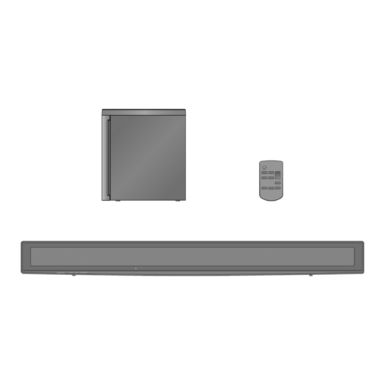
Page 11: Location Of Controls And Components
5 Location of Controls and Components 5.1. Main Unit Key Button Operations... -
Page 12: Remote Control Key Buttons Operation
5.2. Remote Control Key Buttons Operation 5.3. Audio Information... -
Page 13: Self Diagnostic And Special Mode Setting
6 Self diagnostic and special mode setting This unit is equipped with features of self-diagnostic & special mode setting for checking the functions & reliability. Special Note : Checking of the reliability (ageing) & changer operation must be carry out to ensure good working condi- tion in unit. -
Page 14: Service Mode
6.2. Service Mode This mode can be used during servicing. Here are the procedures to enter into service mode: Step 1 : Power-up the main unit. Step 2 : Press & hold [VOL+] button, [VOL-] button and [POWER] button on main unit. This unit is equipped with service mode function for: Step 1 : Checking the region/model and generation no. - Page 15 6.2.1.4. Firmware version Bit No. (Bit 0~4) It is to indicate the firmware version no. (Bit 0 ~4). (Refer to table 6-6 for more information). Bit 4 Bit 3 Bit 2 Bit 1 Bit 0 Version No DPLII DOLBY PCM/AAC Table 6-6...
- Page 16 6.2.2. Checking of HDMI Micro-p Firmware version Here are the procedures for checking the HDMI micro-p firmware version no: Step 1 : Enter into service mode. (Refer to Section 6.2 for the procedures) Step 2 : Press [VOL-] to check the region no. (Refer to table 6-7 for information). Step 3 : Press [VOL-] to check the HDMI micro-p firmware version no.
- Page 17 6.2.2.4. Firmware version Bit No. (Bit 0~4) It is to indicate the firmware version no. (Bit 0 ~4). (Refer to table 6-9 for more information). Bit 4 Bit 3 Bit 2 Bit 1 Bit 0 Version No DPLII DOLBY PCM/AAC Table 6-11 6.2.3.
-
Page 18: Service Fixture & Tools
7 Service Fixture & Tools Prepare service tools before proccess service position. Ref. No. Service Tools Remarks SFT1 Main P.C.B. (CN700) - SMPS P.C.B. (H2016) REXX1103 (10P Cable Wire) -
Page 19: Disassembly And Assembly Instructions
8 Disassembly and Assembly Instructions Caution Note: • This section describes the disassembly and/or assembly procedures for all major printed circuit boards & main components for the unit. (You may refer to the section of “Main components and P.C.B Locations” as described in the service manual) •... -
Page 20: Disassembly Flow Chart
8.1. Disassembly flow chart The following chart is the procedure for disassembling the casing and inside parts for internal inspection when carrying out the ser- vicing. To assemble the unit, reverse the steps shown in the chart below. 8.2. Main Parts Location Diagram... -
Page 21: Disassembly Of Back Cabinet Assembly
8.3. Disassembly of Back Cabinet Assembly Step 1 : Remove 2 screws. Step 2 : Remove the TV Stand Cover as arrow shown. Step 3 : Remove 4 Screw Covers. - Page 22 Step 4 : Remove 3 screws. Step 5 : Remove 18 screws. Step 6 : Lift up and flip over the Back Cabinet Assembly as arrow shown. Caution : Do not exert too much force as it may damage the wiring within.
- Page 23 8.3.1. Wire Dressing for assembling Step 1 : Ensure Front Speaker L (SP1) wire is properly dressed into the Front Panel Assembly ribs. Step 2 : Ensure Front Speaker L (SP1) wire is properly dressed into the Front Panel Assembly gap and rib. Step 3 : Ensure Front Speaker R (SP2) wire is properly dressed into the Front Panel Assembly rib and gap.
- Page 24 Step 5 : Ensure Front Speaker R (SP2) wire is properly dressed into the Front Panel Assembly ribs. Step 6 : Ensure Front Speaker R (SP2) wire is properly dressed into the Front Panel Assembly gap. Step 7 : Ensure 2P Wire (Wireless-Main) is properly dressed into the Front Panel Assembly rib. Step 8 : Ensure 2P Wire (Wireless-Main) is properly dressed into the Front Panel Assembly gab.
- Page 25 Step 9 : Ensure 2P Wire (Wireless-Main) is properly dressed into the Front Panel Assembly ribs. Step 10 : Ensure 2P Wire (Wireless-Main) is properly dressed into the Front Panel Assembly gaps. Step 11 : Paste 2 pieces of himelons over the wires. Step 12 : Ensure 4P Wire Blue Socket must be dressed facing toward right direction as shown.
-
Page 26: Disassembly Of Wireless Adapter P.c.b
8.4. Disassembly of Wireless Adapter P.C.B. • Refer to “Disassembly of Back Cabinet Assembly”. Step 1 : Remove 2 screws. Step 2 : Detach 14P FFC of connector (CN101) on Tx Card Chassis Unit. Step 3 : Disconnect the 4P Wire White Socket. - Page 27 Step 4 : Flip over the Tx Card Chassis Unit as arrow shown. Step 5 : Remove 1 screw. Step 6 : Release the catches. Step 7 : Remove the Wireless Adapter P.C.B. as arrow shown. Caution : During assembling, ensure the Wireless Adapter P.C.B. is properly seated onto the locators. Caution 1 : During assembling, ensure the 14P FFC must be dressed flatly onto the Front Cabinet Assembly.
-
Page 28: Disassembly Of Front Speaker L (Sp1)
8.5. Disassembly of Front Speaker L (SP1) • Refer to “Disassembly of Back Cabinet Assembly”. Step 1 : Detach the Red (+) and Black (-) speaker wires. Step 2 : Remove 4 screws. Step 3 : Remove the Front Speaker L (SP1). -
Page 29: Disassembly Of Front Speaker R (Sp2)
8.6. Disassembly of Front Speaker R (SP2) • Refer to “Disassembly of Back Cabinet Assembly”. Step 1 : Detach the Red (+) and Black (-) speaker wires. Step 2 : Remove 4 screws. Step 3 : Remove the Front Speaker R (SP2). -
Page 30: Disassembly Of Main Chassis Assembly
8.7. Disassembly of Main Chassis Assembly • Refer to “Disassembly of Back Cabinet Assembly”. Step 1 : Disconnect the 4P Wire Blue Socket and 4P Wire White Socket. Caution 1 : During assembling, ensure 4P Wire White Socket must be dressed facing toward left direction as shown. Caution 2 : During assembling, ensure 4P Wire Blue Socket must be dressed facing toward right direction as shown. - Page 31 Step 2 : Place the Main Chassis Assembly beside the Front Panel Assembly as arrow shown. Step 3 : Detach 12P FFC of the connector (CN300) on Main P.C.B. Step 4 : Detach 14P FFC of the connector (CN100) on Main P.C.B. Step 5 : Remove Main Chassis Assembly.
- Page 32 Caution 1 : Before assembling the Main Chassis Assembly, ensure the FFC of the connector (CN350) is properly bend at supporting tape area. Caution 2 : During assembling, ensure the Main Chassis Assembly is seated properly onto the locators.
-
Page 33: Disassembly Of Led P.c.b. And Panel Tact Switch P.c.b
8.8. Disassembly of LED P.C.B. and Panel Tact Switch P.C.B. • Refer to “Disassembly of Back Cabinet Assembly”. • Refer to “Disassembly of Main Chassis Assembly”. Step 1 : Remove 4 screws and detach Panel Tact Switch P.C.B.. Step 2 : Slightly detach the Panel Tact Switch P.C.B. from Front Panel Assembly. Step 3 : Remove 3 screws. - Page 34 Caution 1 : During assembling, ensure the LED P.C.B. is seated properly onto the locator. Caution 2 : During assembling, ensure the 3P Cable Wire is properly dressed behind Front Panel Assembly rib.
-
Page 35: Disassembly Of Ac Inlet P.c.b
8.9. Disassembly of AC Inlet P.C.B. • Refer to “Disassembly of Back Cabinet Assembly”. • Refer to “Disassembly of Main Chassis Assembly”. Step 1 : Cut off the Cable Tie. Caution : During assembling, ensure the head of cable tie must be facing inward and tail of cable tie must be properly cut with remaining 1mm away from the head. - Page 36 Step 4 : Desolder the wires, black (TL20) and red (TL10). Step 5 : Remove the AC Inlet P.C.B. as arrow shown. Caution : During assembling, ensure the cable wire is properly seated onto the hook.
-
Page 37: Disassembly Of Main P.c.b
8.10. Disassembly of Main P.C.B. • Refer to “Disassembly of Back Cabinet Assembly”. • Refer to “Disassembly of Main Chassis Assembly”. • Refer to (Step 1) to (Step 3) of “Disassembly of AC Inlet P.C.B.”. Step 1 : Remove the PC Sheet Assembly as arrow shown. Step 2 : Remove 2 screws. - Page 38 Step 3 : Detach the 50P FFC of the connector (CN200) on Main P.C.B.. Step 4 : Detach the 12P FFC of the connector (CN300) on Main P.C.B.. Step 5 : Detach the 14P FFC of the connector (CN100) on Main P.C.B.. Step 6 : Slightly push forward the Main P.C.B.
- Page 39 Step 8 : Detach the 10P Cable Wire of the connector (CN700) on Main P.C.B.. Step 9 : Remove the Main P.C.B.. Caution : During assembling, ensure the 10P wire must be properly dressing as diagram shown.
-
Page 40: Disassembly Of Smps P.c.b
8.11. Disassembly of SMPS P.C.B. • Refer to “Disassembly of Back Cabinet Assembly”. • Refer to “Disassembly of Main Chassis Assembly”. Step 1 : Release the Wire from the hook. Caution : During assembling, ensure the cable wire is properly slot into the hook. Step 2 : Remove 2 screws. - Page 41 Step 6 : Remove 1 screw. Step 7 : Detach the 10P Cable Wire of the connector (CN700) on Main P.C.B.. Step 8 : Lift up the SMPS P.C.B.. Caution : During assembling, ensure the SMPS P.C.B. is properly seated onto the locators.
- Page 42 Step 9 : Desolder the wires, black (TL4) and red (TL3). Step 10 : Remove the SMPS P.C.B..
-
Page 43: Replacement Of Switch Regulator Ic (Ic5701)
8.12. Replacement of Switch Regulator IC (IC5701) • Refer to “Disassembly of SMPS P.C.B.”. 8.12.1. Disassembly of Switch Regulator Step 3 : Remove the Switch Regulator IC (IC5701). IC (IC5701) Step 1 : Desolder pins of the Switch Regulator IC (IC5701) on the solder side of SMPS P.C.B.. - Page 44 8.12.2. Assembly of Switch Regulator IC Step 4 : Solder pins of Switch Regulator IC (IC5701) on the sol- der side of SMPS P.C.B.. (IC5701) Step 1 : Apply Grease on the Heatsink Unit B. Step 2 : Mount the Switch Regulator IC (IC5701) onto the SMPS P.C.B..
-
Page 45: Replacement Of Rectifier Diode (D5802)
8.13. Replacement of Rectifier Diode (D5802) • Refer to “Disassembly of SMPS P.C.B.”. 8.13.1. Disassembly of Rectifier Diode Step 3 : Remove the Rectifier Diode (D5802) from the Heatsink Unit A. (D5802) Step 1 : Desolder pins of the Rectifier Diode (D5802) on the solder side of SMPS P.C.B.. - Page 46 8.13.2. Assembly Rectifier Diode Step 4 : Solder pins of the Rectifier Diode (D5802) on the sol- der side of SMPS P.C.B.. (D5802) Step 1 : Apply Grease on the Heatsink Unit A. Step 2 : Mount the Rectifier Diode (D5802) onto the SMPS P.C.B..
-
Page 47: Disassembly Of Hdmi P.c.b
8.14. Disassembly of HDMI P.C.B. • Refer to “Disassembly of Back Cabinet Assembly”. • Refer to “Disassembly of Main Chassis Assembly”. • Refer to (Step 1) - (Step 5) of “Disassembly of SMPS P.C.B.”. Step 1 : Detach the 50P FFC of the connector (CN1001) on HDMI P.C.B.. Step 2 : Remove 3 screws. - Page 48 Step 3 : Remove 2 screws. Step 4 : Lift up the HDMI P.C.B. Unit as arrow shown. Caution : During assembling, ensure the HDMI P.C.B. Unit is properly seated onto the locators.
- Page 49 Step 5 : Desolder the 2 legs of Shield Plate Unit. Step 6 : Desolder the 2 legs of Shield Plate Unit. Step 7 : Remove the HDMI P.C.B. Chassis as arrow shown.
-
Page 50: Service Position
9 Service Position Note: For description of the disassembly procedures, see the Section 8. 9.1. Checking and Repairing of Main P.C.B. (Side A) Step 1 : Remove Back Cabinet Assembly. Step 2 : Remove AC Inlet P.C.B.. Step 3 : Remove the PC Sheet Assembly. Step 4 : Main P.C.B. -
Page 51: Checking And Repairing Of Main P.c.b. (Side B)
9.2. Checking and Repairing of Main P.C.B. (Side B) Step 1 : Remove Back Cabinet Assembly. Step 2 : Remove Main Chassis Assembly. Step 3 : Remove AC Inlet P.C.B.. Step 4 : Remove the PC Sheet Assembly. Step 5 : Remove Main P.C.B.. Step 6 : Connect 10P Cable Wire of connector (CN700) on Main P.C.B.. -
Page 52: Checking And Repairing Of Wireless Adapter P.c.b
9.3. Checking and Repairing of Wireless Adapter P.C.B. Step 1 : Remove Back Cabinet Assembly. Step 2 : Remove 2 screws. Step 3 : Flip over the Tx Card Chassis Unit as arrow shown. Step 4 : Wireless Adapter P.C.B. can be checked and repaired as diagram shown. -
Page 53: Checking And Repairing Of Smps P.c.b
9.4. Checking and Repairing of SMPS P.C.B. Step 1 : Remove Back Cabinet Assembly. Step 2 : Remove Main Chassis Assembly. Step 3 : Remove SMPS P.C.B.. Step 4 : Connect 4P Wire Blue Socket. Step 5 : Connect 4P Wire White Socket. - Page 54 Step 6 : Flip the SMPS P.C.B. as arrow shown. Step 7 : Connect 10P Cable Wire to connector (CN700) with 10P Extension Cable Wire (SFT1). Step 8 : SMPS P.C.B. can be checked and repaired as diagram shown.
-
Page 55: Checking And Repairing Of Hdmi P.c.b. (Side A)
9.5. Checking and Repairing of HDMI P.C.B. (Side A) Step 1 : Remove Back Cabinet Assembly. Step 2 : Remove Main Chassis Assembly. Step 3 : Remove the HDMI P.C.B.. Step 4 : Attach the 50P FFC of the connector (CN1001) on HDMI P.C.B.. Step 5 : Connect 10P Cable Wire to connector (CN700) with 10P Extension Cable Wire (SFT1). -
Page 56: Checking And Repairing Of Hdmi P.c.b. (Side B)
9.6. Checking and Repairing of HDMI P.C.B. (Side B) • Refer to (Step 1) to (Step 7) of “Checking and Repairing of HDMI P.C.B. (Side A)”. Step 1 : Flip the HDMI P.C.B. as arrow shown. Step 2 : HDMI P.C.B. (Side B) can be checked and repaired as diagram shown. -
Page 57: Voltage Measurement & Waveform Chart
10 Voltage Measurement & Waveform Chart Note: • Indicated voltage values are the standard values for the unit measured by the DC electronic circuit tester (high-impedance) with the chassis taken as standard. Therefore, there may exist some errors in the voltage values, depending on the internal impedance of the DC circuit tester. •... -
Page 58: Hdmi P.c.b. (2/5)
10.2. HDMI P.C.B. (2/5) IC1002 REF NO. MODE CD PLAY STANDBY IC1003 REF NO. MODE CD PLAY STANDBY IC1004 REF NO. MODE CD PLAY STANDBY IC1005 REF NO. MODE CD PLAY STANDBY IC1006 REF NO. MODE CD PLAY STANDBY REF NO. IC1006 MODE CD PLAY... -
Page 59: Hdmi P.c.b. (3/5)
10.3. HDMI P.C.B. (3/5) REF NO. IC2002 MODE CD PLAY STANDBY IC2002 REF NO. MODE CD PLAY STANDBY REF NO. IC2002 MODE CD PLAY STANDBY IC2003 REF NO. MODE CD PLAY STANDBY REF NO. IC2004 MODE CD PLAY STANDBY IC2006 REF NO. -
Page 60: Hdmi P.c.b. (4/5)
10.4. HDMI P.C.B. (4/5) IC2101 REF NO. MODE CD PLAY STANDBY IC2101 REF NO. MODE CD PLAY STANDBY IC2102 REF NO. MODE CD PLAY STANDBY IC2231 REF NO. MODE CD PLAY STANDBY IC2232 REF NO. MODE CD PLAY STANDBY IC2232 REF NO. -
Page 61: Hdmi P.c.b. (5/5)
10.5. HDMI P.C.B. (5/5) REF NO. IC2232 MODE CD PLAY STANDBY IC2232 REF NO. MODE CD PLAY STANDBY IC2233 REF NO. MODE CD PLAY STANDBY IC4722 REF NO. MODE CD PLAY STANDBY IC4724 REF NO. MODE CD PLAY 18.0 STANDBY 18.0 IC4793 REF NO. -
Page 62: Main P.c.b. (1/2)
10.6. MAIN P.C.B. (1/2) REF NO. IC107 MODE CD PLAY STANDBY IC401 REF NO. MODE CD PLAY STANDBY IC401 REF NO. MODE CD PLAY STANDBY IC401 REF NO. MODE CD PLAY STANDBY IC401 REF NO. MODE CD PLAY STANDBY IC405 REF NO. -
Page 63: Main P.c.b. (2/2)
10.7. MAIN P.C.B. (2/2) REF NO. IC604 MODE CD PLAY STANDBY IC604 REF NO. MODE CD PLAY STANDBY IC604 REF NO. MODE CD PLAY STANDBY IC605 REF NO. MODE CD PLAY STANDBY IC606 REF NO. MODE CD PLAY STANDBY IC700 REF NO. -
Page 64: Smps P.c.b
10.9. SMPS P.C.B. REF NO. IC5701 MODE CD PLAY 159.3 17.5 STANDBY 159.3 17.5 IC5799 REF NO. MODE CD PLAY 12.3 165.0 STANDBY 12.3 165.0 IC5801 REF NO. MODE CD PLAY 18.3 STANDBY 18.3 IC5899 REF NO. MODE CD PLAY STANDBY Q5720 Q5841... -
Page 65: Waveform Chart (1/2)
10.11. Waveform Chart (1/2) 2Vp-p(20nsec/div) 1Vp-p(20nsec/div) 3.2Vp-p(500nsec/div) 6Vp-p(1usec/div) 6Vp-p(1usec/div) 32Vp-p(1usec/div) 2.6Vp-p(50nsec/div) 6Vp-p(1usec/div) 2Vp-p(50nsec/div) 2Vp-p(20nsec/div) 1.7Vp-p(20nsec/div) 3.4Vp-p(5usec/div) 3.6Vp-p(10usec/div) 6Vp-p(2usec/div) 6.4Vp-p(2usec/div) 8Vp-p(1usec/div) 0.2Vp-p(5msec/div) 6.4Vp-p(2usec/div) 4Vp-p(2nsec/div) 2.4Vp-p(200nsec/div) -
Page 66: Waveform Chart (2/2)
10.12. Waveform Chart (2/2) 3Vp-p(200nsec/div) 0.5Vp-p(10usec/div) 3.8Vp-p(100nsec/div) 3Vp-p(20usec/div) 2.6Vp-p(100nsec/div) 6.8Vp-p(1usec/div) 3.4Vp-p(5usec/div) 5.2Vp-p(1usec/div) 5.2Vp-p(500nsec/div) 3.6Vp-p(5usec/div) 6Vp-p(1usec/div) 5Vp-p(5usec/div) 3.4Vp-p(5usec/div) 3Vp-p(20nsec/div) 1Vp-p(20nsec/div) -
Page 67: Illustration Of Ic's, Transistors And Diodes
11 Illustration of IC’s, Transistors and Diodes C0FBZK000013 (64P) C1AB00002989 (144P) C0JBAQ000073 (18P) C2HBCY000030 (128P) C1AB00002975 (100P) C0JBAZ001466 (20P) C1AB00003216 (64P) C1AB00003217 (44P) C3ABMG000238 (50P) No.1 No.1 No.1 RFKWMHTB10PB C0CBCBC00049 C0CBABC00117 C0JBAR000396 C2CBDD000001 C0EBG0000107 RFKWMHTB500P C0CBCDC00014 C0JBAB000986 C3EBEC000047 MIP2F20MSSCF C0CBCAG00015 C0DAAMH00013 C0DAEMZ00001 2SC3940ARA... -
Page 68: Overall Simplified Block
12 Overall Simplified Block... -
Page 69: Block Diagram
13 Block Diagram 13.1. SYSTEM CONTROL BLOCK DIAGRAM MAIN P.C.B. HDMI P.C.B. CN1001 CN200 REMOTE IC604 RFKWMHTB500P MICRO PROCESSOR FROM SDET SDET S DET POWER SUPPLY LED P.C.B. Z300 REMOTE CONTROL SENSOR REMOTE 5 REMOTE CN300 CN350 REMOCON REMOTE 19 VREF XIN 15 ECO DAMP... -
Page 70: Hdmi Block Diagram
13.2. HDMI BLOCK DIAGRAM : HDMI AUDIO INPUT SIGNAL LINE : HDMI VIDEO INPUT SIGNAL LINE : AUDIO OUTPUT SIGNAL LINE : VIDEO OUTPUT SIGNAL LINE HDMI P.C.B. IC2003 IC2002 C3EBEC000047 RFKWMHTB10PB EEPROM MICRO PROCESSOR SCL 6 IDROM CK DCDET DCDET 54 DCDET SDA 5... -
Page 71: Audio (1/2) Block Diagram
13.3. AUDIO (1/2) BLOCK DIAGRAM : OPTICAL/HDMI AUDIO INPUT SIGNAL LINE : AUDIO OUTPUT SIGNAL LINE HDMI P.C.B. MAIN P.C.B. IC1002 C0FBZK000013 CODEC JK4101 OPTICAL DIGITAL AUDIO IN INPUT 3 RXP7 (TV) TO AUDIO SECTION (2/2) CN1001 CN200 IC1005 DT OUT CODEC CDOUT 8 FROM/TO C0JBAR000396... -
Page 72: Audio (2/2) Block Diagram
13.4. AUDIO (2/2) BLOCK DIAGRAM : OPTICAL/HDMI AUDIO INPUT SIGNAL LINE : AUDIO OUTPUT SIGNAL LINE WIRELESS ADAPTER P.C.B. MAIN P.C.B. DIGITAL TRANSMITTER CN100 CN101 CN100 WCLK CN100 CN101 CN100 BCLK DSP SD3 ADAT0 CN100 CN101 CN100 TO AUDIO SECTION (1/2) IC401 C1AB00003216 DIGITAL AUDIO PWM PROCESSOR... -
Page 73: Ic Terminal Chart (Hdmi/Audio)
13.5. IC TERMINAL CHART (HDMI/AUDIO) IC2232 IC2101 JK2203 IC2232 IC1001 IC1006 HDMI RECEIVER HDMI TRANSMITTER HDMI AV IN (BD/DVD) HDMI RECEIVER SDRAM SIGNAL NAME SIGNAL NAME SIGNAL NAME Port Name Pin No Pin No Port Name Port Name Pin No Pin No Port Name Port Name... -
Page 74: Power Supply (1/2) Block Diagram
13.6. POWER SUPPLY (1/2) BLOCK DIAGRAM IC5799 SMPS P.C.B. MAIN P.C.B. MIP2F20MSSCF T5751 SWITCHING POWER SUPPLY CONTROL TRANSFORMER D5896 TR 3 SYS5V H2016* CN700 SYS6V SYS6V D5798 VCC 4 IC700 C0CBABC00117 VOLTAGE REGULATOR SYS3.3V SYS3.3V 3 IN OUT 1 3.3V IC5899 C0DAEMZ00001 SHUNT... -
Page 75: Power Supply (2/2) Block Diagram
13.7. POWER SUPPLY (2/2) BLOCK DIAGRAM MAIN P.C.B. HDMI P.C.B. CN200 CN1001 BK3.3V BK3.3V BK3.3V 3.3V 20,21 30,31 IC4793 D2006 C0CBCDC00014 VOLTAGE REGULATOR 1 VIN BK5V BK5V CN200 CN1001 SYS6V SYS6V VOUT 5 3 VC 1,2,3 48,59,50 SDET CN200 CN1001 DCDET IC2004 C0CBCBG00013... -
Page 77: Wiring Connection Diagram
14 Wiring Connection Diagram CAUTION RISK OF ELECTRIC SHOCK AC VOLTAGE LINE. PLEASE DO NOT TOUCH THIS P.C.B CN300 CN100 CN401* SPEAKERS (FRONT) CN700 MAIN P.C.B. (SIDE B) TL4* H2016* T5703 (MAIN TRANSFORMER) TL3* SMPS P.C.B. CN402* CN600 (FOR ON BOARD PROGRAMMING) CN200 SOLDER SIDE... -
Page 79: Schematic Diagram Notes
15 Schematic Diagram Notes • Voltage and Signal lines: : +B signal line (All schematic diagrams may be modified at any time with the development of new technology) : -B signal line Notes: S300: POWER switch ( : Audio Output signal line S301: VOLUME UP switch (VOLUME +). -
Page 81: Schematic Diagram
16 Schematic Diagram 16.1. HDMI CIRCUIT (1/6) SCHEMATIC DIAGRAM - 1 HDMI CIRCUIT : +B SIGNAL LINE : HDMI/OPTICAL AUDIO INPUT SIGNAL LINE : HDMI VIDEO INPUT SIGNAL LINE : AUDIO OUTPUT SIGNAL LINE : VIDEO OUTPUT SIGNAL LINE IC1003 LB2002 J0JBC0000072 C0CBCAG00015... -
Page 82: Hdmi Circuit (2/6)
16.2. HDMI CIRCUIT (2/6) SCHEMATIC DIAGRAM - 2 HDMI CIRCUIT : +B SIGNAL LINE : HDMI/OPTICAL AUDIO INPUT SIGNAL LINE : HDMI VIDEO INPUT SIGNAL LINE : AUDIO OUTPUT SIGNAL LINE : VIDEO OUTPUT SIGNAL LINE LB4101 J0JBC0000014 D3.3V JK4101 C4101 0.01 C4104... -
Page 83: Hdmi Circuit (3/6)
16.3. HDMI CIRCUIT (3/6) SCHEMATIC DIAGRAM - 3 HDMI CIRCUIT : +B SIGNAL LINE : HDMI/OPTICAL AUDIO INPUT SIGNAL LINE : HDMI VIDEO INPUT SIGNAL LINE : AUDIO OUTPUT SIGNAL LINE : VIDEO OUTPUT SIGNAL LINE MODE RESET1 QR2002 IC1008 B1GBCFJJ0007 D2001 C2CBDD000001... -
Page 84: Hdmi Circuit (4/6)
16.4. HDMI CIRCUIT (4/6) SCHEMATIC DIAGRAM - 4 HDMI CIRCUIT : +B SIGNAL LINE : HDMI/OPTICAL AUDIO INPUT SIGNAL LINE : HDMI VIDEO INPUT SIGNAL LINE : AUDIO OUTPUT SIGNAL LINE : VIDEO OUTPUT SIGNAL LINE TO HDMI R2085 SECTION (1/6) IC2081 C0JBAB000986 C2083... -
Page 85: Hdmi Circuit (5/6)
16.5. HDMI CIRCUIT (5/6) SCHEMATIC DIAGRAM - 5 HDMI CIRCUIT : +B SIGNAL LINE : HDMI/OPTICAL AUDIO INPUT SIGNAL LINE : HDMI VIDEO INPUT SIGNAL LINE : AUDIO OUTPUT SIGNAL LINE : VIDEO OUTPUT SIGNAL LINE TO HDMI SECTION (2/6) C2276 C2278 JK2203... -
Page 86: Hdmi Circuit (6/6)
16.6. HDMI CIRCUIT (6/6) SCHEMATIC DIAGRAM - 6 HDMI CIRCUIT : +B SIGNAL LINE : HDMI/OPTICAL AUDIO INPUT SIGNAL LINE : HDMI VIDEO INPUT SIGNAL LINE : AUDIO OUTPUT SIGNAL LINE : VIDEO OUTPUT SIGNAL LINE TO HDMI SECTION (3/6) LB2005 J0JHC0000021 R4765... -
Page 87: Main Circuit (1/4)
16.7. MAIN CIRCUIT (1/4) SCHEMATIC DIAGRAM - 7 MAIN CIRCUIT : +B SIGNAL LINE : AUDIO OUTPUT SIGNAL LINE R661 R644 C612 1000P LED_DI R681 65 64 60 59 LED_CLK R682 LED_CLK LED_CS R630 H_REQ R683 LED_CS H_REQ HDMI_MUTE R640 R629 REG1 HDMI_MUTE... -
Page 88: Main Circuit (2/4)
16.8. MAIN CIRCUIT (2/4) SCHEMATIC DIAGRAM - 8 MAIN CIRCUIT : +B SIGNAL LINE : AUDIO OUTPUT SIGNAL LINE TO MAIN SECTION (1/4) SP_FL+ C192 1000P R469 CHASSIS C467 25V470 C447 C166 0.01 1000P C446 C165 0.01 1000P R468 SP_FL- C191 1000P WIRELESS ADAPTER... -
Page 89: Main Circuit (3/4)
16.9. MAIN CIRCUIT (3/4) SCHEMATIC DIAGRAM - 9 MAIN CIRCUIT : +B SIGNAL LINE : AUDIO OUTPUT SIGNAL LINE TO MAIN SECTION (1/4) CN200 HDMI_MUTE HDMI_MUTE LB101 CN100 DSP_GND J0JHC0000021 RESET_DSP +12V RESET_DSP +12V MOSI_DSP C101 MOSI_DSP +12V MISO_DSP PGND MISO_DSP BUSY_DSP BUSY_DSP... -
Page 90: Main Circuit (4/4)
16.10. MAIN CIRCUIT (4/4) SCHEMATIC DIAGRAM - 10 MAIN CIRCUIT : +B SIGNAL LINE : AUDIO OUTPUT SIGNAL LINE TO MAIN SECTION (2/4) SYS3.3V IC700 C0CBABC00117 VOLTAGE REGULATOR R236 4.7K LB700 LB701 R179 C158 220K Q116 R180 C700 C701 220K B1ADBL000010 SP_PROTCT DC DETECT... -
Page 91: Led Circuit, Panel Tact Switch Circuit, Ac Inlet Circuit
16.11. LED CIRCUIT, PANEL TACT SWITCH CIRCUIT, AC INLET CIRCUIT SCHEMATIC DIAGRAM - 11 LED CIRCUIT : +B SIGNAL LINE R385 C357 R351 D321 B0ACCK000005 Z300 B3RAC0000019 IC300 CN350 REMOTE CONTROL SENSOR C0JBAQ000073 D320 B0ACCK000005 LED DRIVER R372 R369 R367 R365 R363 R361... -
Page 92: Smps Circuit (1/2)
16.12. SMPS CIRCUIT (1/2) SCHEMATIC DIAGRAM - 12 SMPS CIRCUIT : +B SIGNAL LINE PC5799 B3PBA0000402 FEED BACK R5894 R5890 2.2K R5798 D5798 B0EAMM000057 D5896 C5798 TO SMPS B0JAMF000011 100V10 SECTION (2/2) IC5799 MIP2F20MSSCF SWITCHING POWER SUPPLY CONTROL R5895 R5893 C5898 R5892 C5899... -
Page 93: Smps Circuit (2/2)
16.13. SMPS CIRCUIT (2/2) SCHEMATIC DIAGRAM - 13 SMPS CIRCUIT : +B SIGNAL LINE D5701 B0EBNR000015 D5700 B0EAKT000061 D5703 B0EAKT000062 R5702 100K C5713 0.01 C5711 R5703 100K 200V100 Q5720 D5802 2SC3940ARA B0HBSM000054 HEATSINK* R5720 D5731 REGULATOR B0EAMM000057 R5723 R5722 D5724 D5727 C5700 TO SMPS... -
Page 94: Wireless Adapter Circuit
16.14. WIRELESS ADAPTER CIRCUIT SCHEMATIC DIAGRAM - 14 WIRELESS ADAPTER CIRCUIT : +B SIGNAL LINE : AUDIO OUTPUT SIGNAL LINE TO DIGITAL TRANSMITTER RF_GND RESERVED ADAT3 (NO USE) RESERVED ADAT2 (NO USE) RESERVED ADAT1 (NO USE) RESERVED R130 LB103 CN101 ADAT0 (C/SW) 5V GND J0JBC0000015... -
Page 95: Printed Circuit Board
17 Printed Circuit Board 17.1. HDMI P.C.B. (SIDE A) HDMI P.C.B. (REPX0840D) Q2236 Q2234 Q2233 QR2232 QR2231 Q2232 Q2231 VA2239 R2241 LB2231 R2235 R2234 R2249 R2254 R2238 LB2232 LB4102 R2239 R2243 R2253 LB2233 R2248 R2278 R2240 C2232 LB2234 Q2235 R2237 R2283 C2283 C2254... -
Page 96: Hdmi P.c.b. (Side B)
17.2. HDMI P.C.B. (SIDE B) HDMI P.C.B. (REPX0840D) CN1001 JK2203 R2246 LB2243 IC2231 R2245 R2265 R2072 R2094 IC4724 HDMI AV IN (BD/DVD) LB2241 VA2232 C4773 VA2237 C4770 IC2232 C4366 R2270 R4361 R4776 R4763 R2271 C4367 R2272 R4774 R4775 R4368 R2273 R4362 R2274 C2276... -
Page 97: Main P.c.b. (Side A)
17.3. MAIN P.C.B. (SIDE A) MAIN P.C.B. (REPX0839KA) R468 C165 C803 TL402 C166 C714 C191 IC701 R176 C447 C192 R527 IC702 C186 R705 R184 R708 C701 C181 C709 R709 LB701 R706 R707 R464 C712 IC700 C161 R710 QR601 R526 R465 QR602 C443 QR600... -
Page 98: Main P.c.b. (Side B)
17.4. MAIN P.C.B. (SIDE B) MAIN P.C.B. (REPX0839KA) ZJ402 Q704 CN300 D704 CN100 R103 Q501 L414 C153 R179 L421 R104 C548 D706 R587 R168 C158 D700 TL303 Q500 L422 C303 Q114 Q116 R180 C150 R100 CN401* C708 4-FL- FP700 3-FL+ SPEAKERS L406 C713... -
Page 99: Led P.c.b., Panel Tact Switch P.c.b
17.5. LED P.C.B., PANEL TACT SWITCH P.C.B. LED P.C.B. (REPX0839KB) R384 IC300 R367 R363 C353 0686CB 0686CB (SIDE A) R381 R351 D320 C354 CN350 R383 R365 R382 CN351* C350 C352 R355 R353 R354 0686CB 0686CB C355 Z300 SENSOR (SIDE B) PANEL TACT SWITCH P.C.B. -
Page 100: Ac Inlet P.c.b., Smps P.c.b., Wireless Adapter P.c.b
17.6. AC INLET P.C.B., SMPS P.C.B., WIRELESS ADAPTER P.C.B. AC INLET P.C.B. (REPX0841BA) WIRELESS ADAPTER P.C.B. (REPX0841BC) AC IN 0691BC-4 0691BC-4 120V 60Hz TL102* P5701 R101 TL20* TL10* CN101 TL101* C102 LB106 LB103 ZA5702 CN100 ZA5701 R102 L100 LB105 2.5A 125V IC100 R127 R126... -
Page 101: Terminal Function Of Ic's
18 Terminal Function of IC’s 18.1. IC604 (RFKWMHTB500P) IC MICRO PROCESSOR Port FUNCTION NAME RC_LED Remote control LED Port FUNCTION NAME No Connection W_SSB Wireless SSB No Connection W_DET Wireless Detection No Connection W_INT Wireless TX control VCC2 Main power supply W_CL Wireless Clock DAP_PDN... -
Page 102: Ic2002 (Rfkwmhtb10Pb) Ic Micro Processor
18.2. IC2002 (RFKWMHTB10PB) IC MICRO PROCESSOR Port Function Name No Connection Port Function Name No Connection IN2_5V Detection of connection to No Connection HDMI IN2 No Connection IN1_5V Detection of connection to No Connection HDMI IN1 No Connection No Connection VCC2 Main power supply M_CS... -
Page 103: Exploded View And Replacement Parts List
19 Exploded View and Replacement Parts List 19.1. Exploded View and Mechanical replacement Parts List 19.1.1. Cabinet Parts Location (SU-HTB500) (SMPS P.C.B.) T5751 ZJ5803 *H2016 *TL3 *TL4 (HDMI P.C.B.) CN100 *HEATSINK *CN401 JK4001 UNIT B CN2001 T5703 CN300 JK2101 CN1001 *HEATSINK CN700 UNIT A... - Page 104 19.1.2. Packaging (SC-HTB500) SU-HTB500 A1-1 ACCESSORIES BAG SB-WA500 O/I BOOK PRE SCREW ASS’Y LOCK PIN UNIT F R O N POLYFOAM (LEFT) POLYFOAM (RIGHT) SC-HTB500PPK PACKAGING DRAWINGS...
- Page 105 19.1.3. Mechanical Repacement Parts List Safety Ref. Part No. Part Name & QTY Remarks Description Safety Ref. Part No. Part Name & QTY Remarks RMQX1062-K1 EVA (MAIN CHASSIS) 2 Description RSCX1039-1 AC IN SHIELD UNIT CABINET AND CHAS- XTB3+10JFJ SCREW XTB3+10JFJK SCREW XTB3+16GFJK...
- Page 106 Safety Ref. Part No. Part Name & QTY Remarks Description RMQX1072-K IR BLASTER SPACER (BOTTOM) RMQX1072A-Q IR BLASTER SPACER (TOP) RGKX1041-K TV STAND COVER XTB3+8JFJK SCREW REZX1007-1 14P FFC (MAIN- WIRELESS) RMKX1022-K TX CARD CHASSIS REZX1016 2P WIRE (WIRELESS- MAIN) J0KD00000119 FERRITE CORE RMFX1054A-K HIMELON...
-
Page 107: Electrical Replacement Parts List
19.2. Electrical Replacement Parts List Safety Ref. Part No. Part Name & QTY Remarks Description Safety Ref. Part No. Part Name & QTY Remarks IC2004 C0CBCBG00013 IC Description IC2006 C0JBAZ001466 IC PRINTED CIRCUIT IC2081 C0JBAB000986 IC BOARDS IC2101 C1AB00002975 IC IC2102 C0CBCAG00015 IC PCB1 REPX0840D... - Page 108 Safety Ref. Part No. Part Name & QTY Remarks Safety Ref. Part No. Part Name & QTY Remarks Description Description QR2002 B1GBCFJJ0007 TRANSISTOR VA2109 EZJZ0V80008B VARISTOR QR2004 B1ABMF000020 TRANSISTOR VA2110 EZJZ0V80008B VARISTOR QR2231 B1GBCFJJ0007 TRANSISTOR VA2111 EZJZ0V80008B VARISTOR QR2232 B1GBCFJJ0007 TRANSISTOR VA2112 EZJZ0V80008B VARISTOR QR4703 B1GBCFNN0004 TRANSISTOR VA2113 EZJZ0V80008B VARISTOR...
- Page 109 Safety Ref. Part No. Part Name & QTY Remarks Safety Ref. Part No. Part Name & QTY Remarks Description Description LB104 D0GBR00JA008 0 1/16W TERMINALS LB105 D0GBR00JA008 0 1/16W LB106 J0JBC0000015 INDUCTOR ZJ402 K4CZ01000027 TERMINAL LB1000 J0JHC0000021 INDUCTOR ZJ403 K4CZ01000027 TERMINAL LB1001 J0JHC0000021 INDUCTOR ZJ5803 K4CZ01000027 TERMINAL LB1002 J0JHC0000021 INDUCTOR...
- Page 110 Safety Ref. Part No. Part Name & QTY Remarks Safety Ref. Part No. Part Name & QTY Remarks Description Description R435 D0GB101JA008 100 1/16W RESISTORS R436 D0GB102JA008 1K 1/16W R446 D0GB100JA008 10 1/16W R100 J0JYC0000339 INDUCTOR R447 D0GB100JA008 10 1/16W R101 J0JYC0000339 INDUCTOR R448...
- Page 111 Safety Ref. Part No. Part Name & QTY Remarks Safety Ref. Part No. Part Name & QTY Remarks Description Description R656 D0GB473JA008 47K 1/16W R1037 D0GB330JA008 33 1/16W R657 D0GB101JA008 100 1/16W R1038 D0GB330JA008 33 1/16W R658 D0GB101JA008 100 1/16W R1039 D0GB330JA008 33 1/16W...
- Page 112 Safety Ref. Part No. Part Name & QTY Remarks Safety Ref. Part No. Part Name & QTY Remarks Description Description R2068 D0GB101JA008 100 1/16W R2260 D0GB820JA008 82 1/16W R2069 D0GB101JA008 100 1/16W R2261 D0GB820JA008 82 1/16W R2071 D0GB104JA008 100K 1/16W R2262 D0GB821JA008 820 1/16W...
- Page 113 Safety Ref. Part No. Part Name & QTY Remarks Safety Ref. Part No. Part Name & QTY Remarks Description Description R5842 D0GB152JA008 1.5K 1/16W C359 F1H1H1010005 100pF R5843 D0GD222JA017 2.2K 1/10W C400 F1H1H104A013 0.1uF R5890 D0GB222JA008 2.2K 1/16W C401 F1H1H104A013 0.1uF R5891 ERJ3RBD333V 1/16W...
- Page 114 Safety Ref. Part No. Part Name & QTY Remarks Safety Ref. Part No. Part Name & QTY Remarks Description Description C708 EEEFK1C100R 10uF C1074 F1H1C104A042 0.1uF C709 F1H1C474A008 0.47uF C1075 F1H1C104A042 0.1uF C710 EEE1EA330WR 33uF C1076 F1J1A106A043 10uF C711 EEEFK0J471P 470uF 6.3V C1077...
- Page 115 Safety Ref. Part No. Part Name & QTY Remarks Safety Ref. Part No. Part Name & QTY Remarks Description Description C2244 F1H1H102A219 1000pF C5711 F2B2D1010003 100uF 200V C2245 F1H1H102A219 1000pF C5713 F0C2J1030007 0.01uF 630V C2246 F1H1C104A042 0.1uF C5720 F1H1H1010005 100pF C2247 F1H0J1050013 1uF 6.3V...