
Related Manuals for Xilinx Virtex-II Pro


Summary of Contents for Xilinx Virtex-II Pro
- Page 1 Virtex-II Pro Prototype Platform User Guide UG027 / PN 0402044 (v1.6) October 25, 2002...
- Page 2 Virtex-II Pro Prototype Platform User Guide www.xilinx.com UG027 / PN 0402044 (v1.6) October 25, 2002 1-800-255-7778...
- Page 3 Xilinx, Inc. assumes no obligation to correct any errors contained herein or to advise any user of this text of any correction if such be made. Xilinx, Inc. will not assume any liability for the accuracy or correctness of any engineering or software support or assistance provided to a user.
- Page 4 Virtex-II Pro Prototype Platform User Guide UG027 / PN 0402044 (v1.6) October 25, 2002 The following table shows the revision history for this document. Date Version Revision 03/04/02 Preliminary Xilinx release. 05/29/02 Initial Xilinx release. 06/04/02 Modifications to Figure 1-1.
-
Page 5: Table Of Contents
Online Document ............9 Chapter 1: Virtex-II Pro Prototype Platform Package Contents . - Page 6 Virtex-II Pro Prototype Platform User Guide www.xilinx.com UG027 / PN 0402044 (v1.6) October 25, 2002 1-800-255-7778...
-
Page 7: Preface: About This Manual
Preface About This Manual This manual contains information about the Virtex-II Pro™ Prototype Platform prototype and demonstration boards. Manual Contents This manual contains the following chapters: • Chapter 1, “Virtex-II Pro Prototype Platform,” describes the features and operation of the boards •... -
Page 8: Conventions
Problem Solvers Interactive tools that allow you to troubleshoot your design issues http://support.xilinx.com/support/troubleshoot/psolvers.htm Tech Tips Latest news, design tips, and patch information for the Xilinx design environment http://www.support.xilinx.com/xlnx/xil_tt_home.jsp Conventions This document uses the following conventions. An example illustrates each convention. -
Page 9: Online Document
Virtex-II Red text location in another document Handbook. Go to http://www.xilinx.com Blue, underlined text Hyperlink to a website (URL) for the latest speed files. Virtex-II Pro Prototype Platform User Guide www.xilinx.com UG027 / PN 0402044 (v1.6) October 25, 2002 1-800-255-7778... - Page 10 Preface: About This Manual www.xilinx.com Virtex-II Pro Prototype Platform User Guide 1-800-255-7778 UG027 / PN 0402044 (v1.6) October 25, 2002...
-
Page 11: Chapter 1: Virtex-Ii Pro Prototype Platform
Introduction Virtex-II Pro Prototype Platforms are prototype and demonstration boards that allow designers to investigate and experiment with the features of Virtex-II Pro series FPGAs. This document describes the features and operation of the boards, including how to configure chains of FPGAs and serial PROMs. Prototype Platforms are intended strictly for evaluating the functionality of Virtex-II Pro features and are not intended for A/C characterization or high-speed I/O evaluation. -
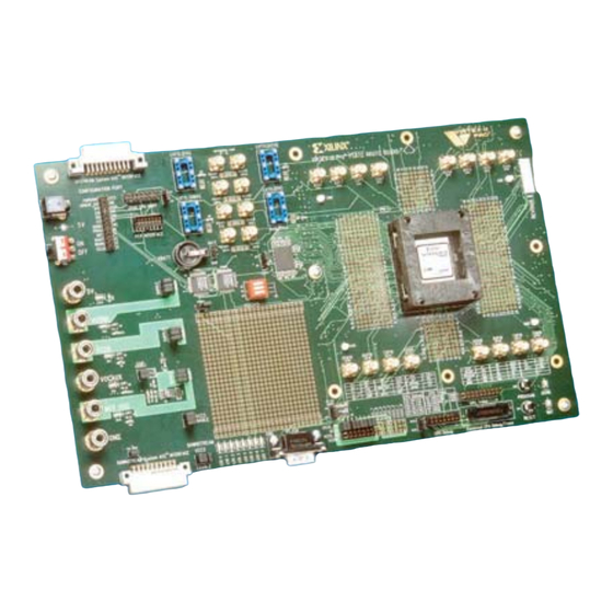
Page 12: Features
The Virtex-II Pro Prototype Platform board (referred to as "the board") contains a DUT FPGA and two in-system XC18V04 programmable SPROMs. Each SPROM can hold up to 4,194,304 bits. - Page 13 VCC Jack 1.5V VCCO VCCO Jack 2.5V VCCAUX AUX Jack 2.5V VCC3 3.3V MGT Jack 2.5V UG027_01_102502 Figure 1-1: Virtex-II Pro Prototype Platform Block Diagram Virtex-II Pro Prototype Platform User Guide www.xilinx.com UG027 / PN 0402044 (v1.6) October 25, 2002 1-800-255-7778...
-
Page 14: Detailed Description
1-2. Each feature is detailed in the numbered sections that follow. Figure 1-2: Detailed Description of Virtex-II Pro Prototype Platform Components 1. Power Switch The board has an onboard power supply and an on|off power switch. When lit, a green LED indicates power from the power brick connector or the 5V jack. -
Page 15: Off Position
Supplies voltage to the V header and the V DUT pins • MGT_VCC ♦ Supplies power to the Rocket I/O transceivers on the DUT (AV AUX, VTT Virtex-II Pro Prototype Platform User Guide www.xilinx.com UG027 / PN 0402044 (v1.6) October 25, 2002 1-800-255-7778... -
Page 16: Configuration Ports
3. Configuration Ports These headers can be used to connect a Parallel Cable III or Parallel Cable IV cable to the board and support all Virtex-II Pro device configuration modes. (See Table 1-3 connecting the cables to the Configuration Ports.) -
Page 17: 5A. Upstream System Ace Connector
DUT. This connector can be sourced by any JTAG configuration stream. For example, a System ACE Controller with CompactFlash can be used to generate very large JTAG streams for configuring multiple Virtex-II Pro Prototype Platforms using the Downstream System ACE connector. -
Page 18: 5B. Downstream System Ace Connector
7. V Enable Supply Jumpers Virtex-II Pro series devices have eight SelectI/O banks, labeled 0 through 7, each with a enable supply jumper. V enable supply jumpers can connect each bank to one of... -
Page 19: Differential Clock Inputs
The device must be oriented using the P1 indicator on the board. Failure to insert the device to the proper orientation can damage the device. To avoid pin damage, always use the vacuum tool provided when inserting or removing the Virtex-II Pro device. When Virtex-II Pro Prototype Platform User Guide www.xilinx.com... -
Page 20: Pin Breakout
Chapter 1: Virtex-II Pro Prototype Platform using BGA packages, do not apply pressure to the device while activating the socket. Doing so can damage the socket and/or the device. 12. Pin Breakout The pin breakout area is used to monitor or apply signals to each of the DUT pins. Headers can be soldered to the breakout area to use with certain types of oscilloscope probes, for either connecting function generators or wiring pins to the pin breakout area. -
Page 21: Reset Switch (Active-Low)
A9, A10 A11, A12 A15, A14 AB15, AB16 AF17, AF18 AP19, AP18 A15, A16 A17, A18 A19, A18 AB9, AB10 AF11, AF12 AP15, AP14 Virtex-II Pro Prototype Platform User Guide www.xilinx.com UG027 / PN 0402044 (v1.6) October 25, 2002 1-800-255-7778... -
Page 22: Sdram Pins
Chapter 1: Virtex-II Pro Prototype Platform 19. SDRAM Pins The system clock that enables proper communication between the SDRAM and the DUT is GCLK1P. Table 1-10 shows the system clock pin locations for the available DUT package types. Table 1-10: System Clock for SDRAM and DUT... - Page 23 3. Disable the SDRAM when using the DUT pins as standard I/O pins. 4. The SDRAM is a Samsung K4S64323LF-S(D)G/S75. For information on its operation, see: http://www.samsungelectronics.com/semiconductors/DRAM/Mobile_SDRAM/64M_bit/K4S64323 LF/ds_k4s64323lf-s(d)g_s.pdf Virtex-II Pro Prototype Platform User Guide www.xilinx.com UG027 / PN 0402044 (v1.6) October 25, 2002 1-800-255-7778...
-
Page 24: Cpu Debug Pins
Chapter 1: Virtex-II Pro Prototype Platform 20. CPU Debug Pins Figure 1-6 shows the location of the CPU debug pins on the debug connector. CPU_TMS CPU_TCK CPU_HALT CPU_TDI CPU_TDO CPU_TRST VCC3/VCCO UG027_06_030402 Figure 1-6: CPU Debug Connector, 16-Pin Male Table 1-12 shows the CPU debug pin locations for the available DUT package types. -
Page 25: Cpu Trace Pins
AG33 TS20 AA22 AE26 AK31 TRC_CLK AB21 AD23 AL34 For details on CPU debug pins, , refer to Appendix A, “RISCWatch and RISCTrace Interfaces.” Virtex-II Pro Prototype Platform User Guide www.xilinx.com UG027 / PN 0402044 (v1.6) October 25, 2002 1-800-255-7778... -
Page 26: Rs232 Port Pins
Chapter 1: Virtex-II Pro Prototype Platform 22. RS232 Port Pins Table 1-14 shows the RS232 port pin locations for the available DUT package types. Table 1-14: RS232 Port Pins FG456 FF672 FF1152 T1IN AF10 T2IN AH10 R1OUT AE11 R2OUT AG10 23. -
Page 27: Appendix A: Riscwatch And Risctrace Interfaces
Position 14 is used as a connection key and does not contain a pin. 0.1" 0.1" UG018_50_100901 Figure A-1: JTAG-Connector Physical Layout Virtex-II Pro Prototype Platform User Guide www.xilinx.com UG027 / PN 0402044 (v1.6) October 25, 2002 1-800-255-7778... - Page 28 1. This signal must be driven by a tri-state device using C405JTGTDOEN as the enable signal. 2. This signal must be inverted between the PPC405x3 and the RISCWatch. www.xilinx.com Virtex-II Pro Prototype Platform User Guide 1-800-255-7778 UG027 / PN 0402044 (v1.6) October 25, 2002...
-
Page 29: Risctrace Interface
No Connect Reserved No Connect Reserved No Connect Reserved No Connect Reserved No Connect Reserved No Connect Reserved No Connect Reserved Output TS1O Execution status. Virtex-II Pro Prototype Platform User Guide www.xilinx.com UG027 / PN 0402044 (v1.6) October 25, 2002 1-800-255-7778... - Page 30 C405TRCODDEXECUTIONSTATUS[1] Output TS2O Input C405TRCEVENEXECUTIONSTATUS[0] Output TS1E Input C405TRCEVENEXECUTIONSTATUS[1] Output TS2E Input C405TRCTRACESTATUS[0] Output Input C405TRCTRACESTATUS[1] Output Input C405TRCTRACESTATUS[2] Output Input C405TRCTRACESTATUS[3] Output Input www.xilinx.com Virtex-II Pro Prototype Platform User Guide 1-800-255-7778 UG027 / PN 0402044 (v1.6) October 25, 2002...