
Related Manuals for Xilinx Virtex-4 FX FPGA


Summary of Contents for Xilinx Virtex-4 FX FPGA
- Page 1 ML42x User Guide Virtex-4 FX FPGA RocketIO Characterization Platform UG087 (v1.3) May 30, 2008 P/N 0402349-02 www.BDTIC.com/XILINX...
-
Page 2: Revision History
Xilinx. Xilinx expressly disclaims any liability arising out of your use of the Documentation. Xilinx reserves the right, at its sole discretion, to change the Documentation without notice at any time. Xilinx assumes no obligation to correct any errors contained in the Documentation, or to advise you of any corrections or updates. -
Page 3: Table Of Contents
11. Xilinx Generic Interface ........ - Page 4 ML42x User Guide UG087 (v1.3) May 30, 2008...
- Page 5 Table 23: System ACE Port Connections ......... 30 www.BDTIC.com/XILINX ML42x User Guide www.xilinx.com...
- Page 6 ML42x User Guide UG087 (v1.3) May 30, 2008...
-
Page 7: Additional Documentation
Additional information is available from the data sheets and application notes from the component manufacturers. Additional Support Resources To search the database of silicon and software questions and answers, or to create a technical support cae WebCase, see the Xilinx website at: http://www.xilinx.com/support. www.BDTIC.com/XILINX ML42x User Guide www.xilinx.com... -
Page 8: Typographical Conventions
Italic font The address (F) is asserted after clock Emphasis in text. event 2. Underlined Text Indicates a link to a web page. http://www.xilinx.com/virtex4 Online Document The following conventions are used in this document: Convention Meaning or Use Example See the section “Additional... -
Page 9: Ml42X Rocketio Characterization Platform
Internet for viewing and printing these files.) • Additional documentation, errata, frequently asked questions, and the latest news • Contents of the CompactFlash card provided with the ML42x platform www.BDTIC.com/XILINX ML42x User Guide www.xilinx.com UG087 (v1.3) May 30, 2008... -
Page 10: Related Documents
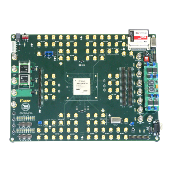
Related Documents Related Documents Prior to using the ML42x platforms, users should be familiar with Xilinx resources. See “References,” page 30 for direct links to Xilinx documentation. See the following locations for additional documentation on Xilinx tools and solutions: •... - Page 11 VCCO Jack VCCINT VCCINT Jack *Note: LVDS headers and clock capable regional clocks VAUX VAUX Jack are not available on ML421 platforms. UG087_01_092006 Figure 1: Virtex-4 FPGA ML42x Platform Block Diagram www.BDTIC.com/XILINX ML42x User Guide www.xilinx.com UG087 (v1.3) May 30, 2008...
-
Page 12: Detailed Description
The image might not reflect the current revision of the board. Note: LVDS headers (12) and clock capable regional clocks (7) are not available on ML421 platforms. UG087_02_102006 Figure 2: Detailed Description of Virtex-4 FPGA ML42x Platform Components www.BDTIC.com/XILINX www.xilinx.com ML42x User Guide UG087 (v1.3) May 30, 2008... -
Page 13: Power Switch
Supplies 3.3V to the System ACE chip and VCC3 3.3V other onboard circuits VCCINT 1.2V J105 Core voltage for the FPGA VCCO 2.5V-3.3V J106 I/O voltage for the FPGA VCCAUX 2.5V Auxiliary supply voltage for the FPGA www.BDTIC.com/XILINX ML42x User Guide www.xilinx.com UG087 (v1.3) May 30, 2008... -
Page 14: Fpga Configuration
CompactFlash memory card can be accessed through the onboard System ACE controller. Note: The System ACE controller is bypassed when the flying wire leads or the Parallel Cable IV cable is used, thus causing no disruption in the JTAG chain. www.BDTIC.com/XILINX www.xilinx.com ML42x User Guide UG087 (v1.3) May 30, 2008... -
Page 15: Oscillator Sockets
Table 6: Differential SMA MGT Clock Pin Connections Label MGT Clock Name ML421 ML423 ML424 MGTCLK110_N AF11 MGTCLK110_P AF10 MGTCLK113_N MGTCLK113_P MGTCLK102_N MGTCLK102_P MGTCLK105_N AF20 AP28 AW33 MGTCLK105_P AF21 AP29 AW34 www.BDTIC.com/XILINX ML42x User Guide www.xilinx.com UG087 (v1.3) May 30, 2008... -
Page 16: Differential Sma Global Clocks
Table 9: User LED, Row 1 (Top) Label ML421 ML423 ML424 DS11 AJ16 AK13 DS12 AG15 AP14 DS13 AF15 AN14 DS14 AF14 AL14 DS15 AE14 AM15 DS16 AE13 AJ14 www.BDTIC.com/XILINX www.xilinx.com ML42x User Guide UG087 (v1.3) May 30, 2008... -
Page 17: User Dip Switches (Active-High)
I/O pins on the FPGA. These pins can be used to set control pins or any other purpose the user designates. Table 11: User DIP Switches, Row 1 (Top) ML421 ML423 ML424 AH15 AJ12 AE11 AP15 AD11 AN15 www.BDTIC.com/XILINX ML42x User Guide www.xilinx.com UG087 (v1.3) May 30, 2008... -
Page 18: User Pushbutton Switches (Active-High)
FPGA. These switches can be used for any purpose that the user designates. Table 13: User Pushbutton Switches Label ML421 ML423 ML424 AH10 AP10 AJ10 AN10 AF10 AJ10 AG10 www.BDTIC.com/XILINX www.xilinx.com ML42x User Guide UG087 (v1.3) May 30, 2008... -
Page 19: Xilinx Generic Interface
Detailed Description 11. Xilinx Generic Interface The XGI is an expansion interface for plug-in modules (for example, the SuperClock module) and provides the user access to the I/O pins listed in Table Table 15, page Table 16, page Table 17, page 21 shows header J10 with all pins connected to V for powering modules tied to this connector. - Page 20 AD13 AK29 AL19 AC14 AJ29 AL21 AC13 AK21 AK19 AC12 AL21 AJ19 AB12 AL29 AM21 AA12 AM30 AM20 X TDO X TDO X TDO VCC3 VCC3 VCC3 VCC3 VCC3 VCC3 www.BDTIC.com/XILINX www.xilinx.com ML42x User Guide UG087 (v1.3) May 30, 2008...
- Page 21 It does not reflect the physical connection to this connector. Table 17: XGI Header (J14) Pin Number ML421 ML423 ML424 www.BDTIC.com/XILINX ML42x User Guide www.xilinx.com UG087 (v1.3) May 30, 2008...
-
Page 22: Lvds Header Interface
Table 18, page 22 Table 19, page 24. These I/O pins can also be used for any purpose designated by the user. Table 18: LVDS Header (J139) Pin Number ML421 ML423 ML424 www.BDTIC.com/XILINX www.xilinx.com ML42x User Guide UG087 (v1.3) May 30, 2008... - Page 23 ML423 ML424 AB11 AH14 AA11 AH13 AD12 AT15 AE12 AU15 AG13 AL13 AH13 AM13 AL10 AU10 AM10 AT10 AJ12 AP11 AK12 AR11 AK13 AK11 AL13 AJ11 AD14 AP16 AC13 AR16 www.BDTIC.com/XILINX ML42x User Guide www.xilinx.com UG087 (v1.3) May 30, 2008...
-
Page 24: Program Switch (Active-Low)
DONE is High, indicating the FPGA is programed or that power is applied to the board without a part in the socket. 16. INIT LED The INIT LED lights during initialization. www.BDTIC.com/XILINX www.xilinx.com ML42x User Guide UG087 (v1.3) May 30, 2008... -
Page 25: System Ace Controller
Pin Name J134 TXN_101A X0Y9 X0Y11 J133 TXP_101A J132 RXN_101A J131 RXP_101A J138 RXN_101B X0Y8 X0Y10 J137 RXP_101B J136 TXN_101B J135 TXP_101B TXN_102A X0Y3 X0Y5 X0Y7 X0Y7 X0Y9 TXP_102A RXN_102A RXP_102A www.BDTIC.com/XILINX ML42x User Guide www.xilinx.com UG087 (v1.3) May 30, 2008... - Page 26 AF24 AP32 AW37 TXN_105B AE26 AM34 AU39 TXP_105B AD26 AL34 AT39 J129 TXN_106A X0Y1 X0Y1 X0Y1 AP22 AW27 J124 TXP_106A AP23 AW28 J130 RXN_106A AP25 AW30 J123 RXP_106A AP26 AW31 www.BDTIC.com/XILINX www.xilinx.com ML42x User Guide UG087 (v1.3) May 30, 2008...
- Page 27 X1Y2 RXP_110B TXN_110B TXP_110B J143 TXN_111A X1Y5 J142 TXP_111A J141 RXN_111A J140 RXP_111A J147 RXN_111B X1Y4 J146 RXP_111B J145 TXN_111B J144 TXP_111B TXN_112A X1Y3 X1Y5 X1Y5 X1Y7 TXP_112A RXN_112A RXP_112A www.BDTIC.com/XILINX ML42x User Guide www.xilinx.com UG087 (v1.3) May 30, 2008...
- Page 28 RXP_113A RXN_113B X1Y2 X1Y4 X1Y6 X1Y6 X1Y8 RXP_113B TXN_113B TXP_113B J118 TXN_114A X1Y9 X1Y11 J117 TXP_114A J115 RXN_114A J116 RXP_114A J122 RXN_114B X1Y8 X1Y10 J121 RXP_114B J120 TXN_114B J119 TXP_114B www.BDTIC.com/XILINX www.xilinx.com ML42x User Guide UG087 (v1.3) May 30, 2008...
-
Page 29: Rs-232 Port
110. Through a master/slave bias circuit, these externally controlled biases can be shared across all MGT tiles within the MGT column. For more information on Rocket IO external biasing, see the Virtex-4 RocketIO Multi-Gigabit Transceiver User Guide [Ref www.BDTIC.com/XILINX ML42x User Guide www.xilinx.com UG087 (v1.3) May 30, 2008... -
Page 30: System Ace Mpu Port
MPCE# MPOE# MPWE# References UG076, Virtex-4 RocketIO Multi-Gigabit Transceiver User Guide UG070, Virtex-4 FPGA User Guide DS080, System ACE CompactFlash Solution UG091, Xilinx Generic Interface (XGI) SuperClock Module User Guide www.BDTIC.com/XILINX www.xilinx.com ML42x User Guide UG087 (v1.3) May 30, 2008...