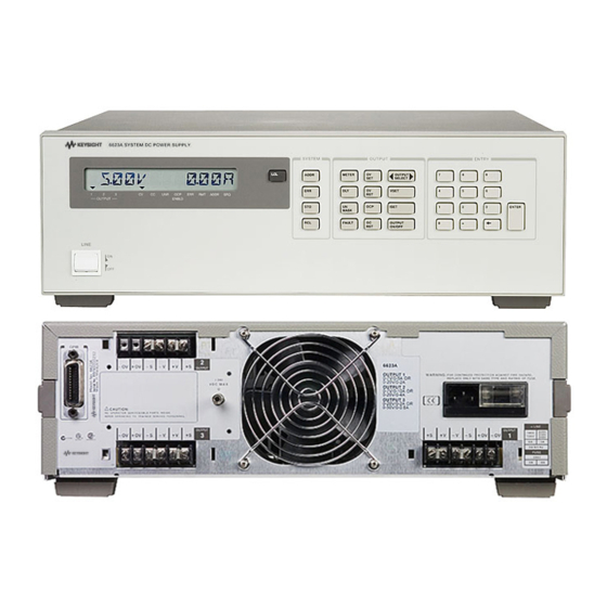
Agilent Technologies 6622A Service Manual
Multiple output linear system
dc power supplies
Hide thumbs
Also See for 6622A:
- Operating manual (115 pages) ,
- Operating instructions manual (14 pages)
Table of Contents
Advertisement
Quick Links
* For instruments with higher Serial Numbers, a change page may be included.
Microfiche Part No. 5957-6380
SERVICE MANUAL
MULTIPLE OUTPUT LINEAR SYSTEM
DC POWER SUPPLIES
Agilent MODELS 6621A, 6622A,
6623A, 6624A, and 6627A
Agilent Part No 5957-6379
Agilent Model 6621A, Serial 3737A-03086 through 03145
Agilent Model 6622A, Serial 3736A-04021 through 04040
Agilent Model 6623A, Serial 3736A-05451 through 05530
Agilent Model 6624A, Serial 3735A-13801 through 14200
Agilent Model 6627A, Serial 3735A-02356 through 02510
5
US37370101 and up
US37360101 and up
US37360101 and up
US37350101 and up
US37350101 and up
Printed in Malaysia: September, 2001
Advertisement
Table of Contents
Troubleshooting

Related Manuals for Agilent Technologies 6622A


Summary of Contents for Agilent Technologies 6622A
- Page 1 6623A, 6624A, and 6627A Agilent Part No 5957-6379 Agilent Model 6621A, Serial 3737A-03086 through 03145 US37370101 and up Agilent Model 6622A, Serial 3736A-04021 through 04040 US37360101 and up Agilent Model 6623A, Serial 3736A-05451 through 05530 US37360101 and up Agilent Model 6624A, Serial 3735A-13801 through 14200...
-
Page 2: Limitation Of Warranty
90 days from date of delivery. During the warranty period Agilent Technologies will, at its option, either repair or replace products which prove to be defective. Agilent does not warrant that the operation for the software, firmware, or hardware shall be uninterrupted or error free. -
Page 3: Safety Summary
Because of the danger of introducing additional hazards, do not install substitute parts or perform any unauthorized modification to the instrument. Return the instrument to an Agilent Technologies Sales and Service Office for service and repair to ensure that safety features are maintained. - Page 4 This statement is provided to comply with the requirements of the German Sound Emission Directive, from 18 January 1991. * Sound Pressure Lp <70 dB(A) * At Operator Position * Normal Operation * According to EN 27779 (Type Test). Edition 2 September, 2001 © Copyright 2001 Agilent Technologies, Inc.
-
Page 5: Table Of Contents
CONTENTS Section I Section IV INTRODUCTION TROUBLESHOOTING SCOPE …....…..……………….......1-1 INTRODUCTION ……………………………………..4-1 SAFETY CONSIDERATIONS …......….1-1 ELECTROSTATIC PROTECTION ………………..…4-1 INSTRUMENT AND MANUAL REMOVAL AND REPLACEMENT …………………4-2 IDENTIFICATION ..……………….……………..1-1 Top Cover Removal …………………………………..4-2 FIRMWARE REVISIONS…...…….......1-2 Gaining Access to Assemblies in the Supply …….…4-2 GPIB Board Removal ………………………………4-2 40 Watt Output Board Removal……………………...4-2... - Page 6 CONTENTS (Cont.) Section VI Appendix A CIRCUIT DIAGRAMS LOGIC SYMBOLOGY INTRODUCTION ………....…..... 6-1 FUNCTIONAL SCHEMATIC DIAGRAMS ..……6-1 COMPONENT LOCATION………………………….6-1...
- Page 7 LIST OF FIGURES Figure Page Agilent 6621A-6624 and 6627A Multiple Output Power Supplies, Block Diagram ………………………………………………2-2 Output Operating Ranges for Agilent Models 6621A-6624A and 6627A ………………………………………………………….2-3 GPIB Board, Block Diagram ……………………………………………………….…………………………………………………2-6 Outpot Board, Secondary Interface Circuits, Block Diagram………………………………………………………………………..2-9 Outpot Board, Power Mesh and Control Circuits, Block …………………………………………………………………………..2-12 Voltage and Current Control Circuits, Simplified Schematic ……………………………………………………………………2-13 Typical Output Range Characteristics ……………………………………………………………………………………………….2-15 Typical Downprogramming Characteristics Below 2.0 V …………………………………………………………………………2-16...
- Page 8 LIST OF TABLES Table Page Test Equipment Required for Verification ……………………………………………………………………………………………3-2 Low Range Voltage and Current Values ……………………………………………………………………………………………3-5 High Range Voltage and Current Values ……………………………………………………………………………………………3-6 Performance Test Record for 40WLV/80WLV Outputs ……………………………………………………………………………3-16 Performance Test Record for 40WHV/80WHV Outputs …………………………………………………………………………3-17 Test Equipment Required for Troubleshooting …………………………………………………………………………………4-5 Fuses ………………………………………………………………………………………………………….…………………………...4-6 Tests Performed at Power-On …………………………………………………………………………………………………………..4-9...
-
Page 9: Section I
INSTRUMENT AND MANUAL IDENTIFICATION NOTE Agilent Technologies instruments are identified by a two- Calibration is generally required after a repair is made. part serial number, i.e. 2601A-00101. The first part of the Software calibration procedures are given in Appendix A serial number (the prefix) is a number/letter combination of the Operating Manual. -
Page 10: Firmware Revisions
week, and the "A" designates the U.S.A. The second part of described in this manual. The yellow change sheet may also the serial number is a different sequential number assigned contain information for correcting errors in the manual. to each instrument. 1-4 FIRMWARE REVISIONS If the serial number prefix on your power supply differs from that shown on the title page of this manual, a yellow... -
Page 11: Principles Of Operation
Section II PRINCIPLES OF OPERATION INTRODUCTION user and the multiple outputs of the power supply. Each output board is actually an output channel that can be individually selected and controlled over the GPIB or from The following paragraphs provide block diagram level the supply's front panel. -
Page 13: Gpib Board (Figure 2-3)
The ac input to each output board is rectified, filtered, and The functional names on the block diagram correspond with applied to the power module regulator. Each output board those on the schematic so that the diagrams can be employs series regulation techniques. The regulator element correlated. -
Page 14: System Microcomputer
System Micro-Computer looks like a 16-bit counter that continuously rolls over and starts at zero. The contents of each address appear The system micro-computer decodes and executes all sequentially on the data bus (other side of the break).In instructions, and controls all data transfers. It consists of a addition, for all signature analysis tests, jumper W201 must microprocessor, an address decoder, RAM and ROM be moved from the NORM RUN position to the SIG... -
Page 15: Front Panel Interface
appears on data bus lines D0-D3, respectively, and selected output board, present function being EEPROM serial output data appears on data bus line D7. programmed, a programmed message, or an error message. Logic 0's will always appear on data bus lines D4-D6 when The annunciators provide operating and status information. -
Page 17: Output Board
2-24 OUTPUT BOARD 2-28 CV DAC. The constant voltage (CV) 12-bit DAC (U313) and amplifier (U315A) convert the digital input into an analog signal (CV REF) in the range of 0 to -10 V. This The following paragraphs provide block diagram level signal is used as a reference voltage and is sent to the descriptions of the output board. - Page 18 The voltage readback buffer (U319C) provides unity gain for flops were reset. The STATUS RESET input line from the the V READBACK signal and isolates the multiplexes circuit microcomputer resets the flip-flops. from the CV control circuit (see Figure 2-5). The current _________ readback amplifier (U345) provides a gain of approximately The status monitor circuit also receives OV SENSE and...
-
Page 20: Power Mesh And Control Circuits
is high, the ON/OFF signal is low and turns off the control 2-37 Power Module Reference Voltage. When the current circuit thus preventing power from reaching the output sources have been turned on, this circuit (P/O U340 and terminals. U337) provides a reference voltage (about 2V above +V) to the power module REF input. - Page 21 SCR, the OVRST command will program the output to the turned off. The bleed circuit is activated via the power-on settings that existed before the OV occurred. circuit when the ON/OFF signal is high. The bleed circuit maintains stability with large output capacitors under light Down Programmer - Separate transistors in the power loading conditions and helps to keep the output impedance module are used to sink output current and are capable of...
- Page 22 2-12...
- Page 23 interface circuit, must be on (approximately + 2 V) in order secondary interface to indicate the magnitude of the output to activate the voltage control circuit. voltage. The voltage control circuit compares the output voltage to If the output voltage exceeds the programmed voltage, the the programmable reference voltage CV REF to produce the summing junction S1 goes negative causing U347 to CV signal.
- Page 24 will conduct less allowing more current to flow into the + resistor R408 is applied to summing junction S3 along with a BASE DRIVE input. This will cause the power module's reference voltage. Based on this summing action, error series regulators to conduct more and thus increase the amplifier U350 generates the - CL control signal which is output voltage.
-
Page 25: Typical Output Range Characteristics
Figure 2-7. Typical Output Range Characteristics 2-15... - Page 26 If the output voltage from + V to exceeds signal can activate the OV DRIVE and shut down the supply programmed overvoltage setting (derived from OV REF), regardless of the state of the POV DISABLE signal. As the overvoltage comparator signal (OV COMP) will activate shown in Figure 2-9, OV TRIP is the output of a wired OR OV DRIVE and fire the SCR provided that the POV signal can gate and can be activated by either the SENSE...
- Page 27 The fixed overvoltage sensing circuit will activate when it Remote Overvoltage Trip - Any output's OV can be triggered senses a voltage that is approximately 120% of the from its ± OV terminals by connection to a remote device maximum rated output voltage for the associated output. If (see Operating Manual) or another output's ±...
- Page 28 2-18...
-
Page 29: Verification
Section III VERIFICATION a. Perform the turn-on and checkout procedures given in INTRODUCTION Section III of the Operating Manual. These procedures include a power-on self test. This section contains test procedures that check the b. Perform the performance tests listed below on each operation of the power supply. -
Page 32: Constant Voltage (Cv) Tests
is considerably easier to use than load resistors. It a. Turn off the supply and connect a digital voltmeter eliminates the need for connecting resistors or rheostats in between the + S and - S terminals of the output to be parallel to handle power, it is much more stable than a tested. - Page 33 * An output channel cannot be programmed to 0 amps. If the output channel receives a command to go to 0 amps (or any positive current below the minimum programmable value), it will set itself to the minimum programmable value. 3-13 CV Load Effect.
- Page 34 * An output channel cannot be programmed to 0 amps. If the output channel receives a command to go to 0 amps (or any positive current below minimum programmable current), will itself programmable current. 3-15 CV Noise (PARD). Periodic and random deviations c.
- Page 35 h. Now observe Channel B on the oscilloscope while 3-17 CV Up Programming Speed. This test measures the maintaining the trigger on Channel A as in step f. Note time required for the output voltage to rise to 63% of the that the diode clamp, used in the test setup of Figure 3- High Range Full Scale Voltage (time constant).
- Page 36 g. Program the output voltage in a loop which alternately c. Program the selected output's voltage to the Low Range programs the output voltage between 0.4 V and the Full Scale Voltage value and the current to the Low High Range Full Scale Voltage value (20 .V for Range Maximum Programmable Current value (see 40WLV/80WLV outputs or 50 V for 40WHV/80WHV Table 3-2).
- Page 37 ± 100 mV. Repeat test by observing the scope after turning off the supply. d. Repeat the test (steps a through c) for each output in your supply. 3-20 Overvoltage Protection. The following tests check the operation and accuracy of the fixed OV, programmable OV, and the external OV protection circuits.
-
Page 38: Constant Current (Cc) Tests
Programmable OV Accuracy Test. This test checks the d. Note the display should indicate "OVERVOLTAGE" for overvoltage (OV) programming accuracy. Taking the OV all outputs. programming accuracy and the voltage programming e. Reset all outputs by turning the supply off and on accuracy into account, the upper and lower limits of the OV again. - Page 39 d. Multiply voltage drop across current output is in negative current limit operation. It also checks monitoring resistor by 10 to convert to amps and record that the negative current limit has two different values this value (Io). Note also the current reading on the depending upon the output voltage.
- Page 40 g. Repeat this test (steps a through f) for each output in your supply. 3-26 CC Source Effect. This test measures the change in output current that results when the ac line voltage changes from the minimum to the maximum value within the specifications.
-
Page 41: Extended Tests
c. Program the current of the selected output to 1.9 amps e. Adjust the transformer to 13% below the nominal line and the output voltage to 20.2 volts by sending the voltage. following strings: f. Wait 30 minutes for the output to stabilize under these initial conditions and then record the output voltage ISET <... -
Page 42: Temperature Coefficient (Tc) Tests
i. Close the short switch and immediately record the f. Observe and record the output current reading output current. periodically over an 8 hour period. The difference j. Wait 30 minutes and again record the output current. between any two readings should be less than the value The difference in the readings taken in steps i and j listed below for the particular output type tested. -
Page 43: Output Current And Readback Current Tc
j. Repeat steps a through i for each output in your supply. g. Repeat steps a through f for each output in your supply. 3-37 Output Current and Readback Current TC 3-38 Negative Current Limit (-CC) a. Repeat steps a through d of paragraph 3-33. Readback TC b. - Page 44 3-16...
- Page 45 3-17...
-
Page 46: Troubleshooting
Section IV TROUBLESHOOTING static charge, even though complete failure may not occur. The following precautions should be observed when handling static-sensitive devices. Most of the maintenance procedures given in this section are performed with power applied and a. Always turn power off before removing or installing protective covers removed. -
Page 47: Removal And Replacement
j. Use a mildly activated rosin core solder (such as Alpha b. Spread the bottom rear of the cover slightly and pull Metal Reliacor No. 1, Agilent Part No. 8090-0098) for back to disengage it from the front panel. repair. The flux residue of this type of solder can be left c. -
Page 49: Replacing The Power Module U338 (U339)
Use the long heat sink screws and M4 nuts to temporarily hold the assembly to the board while Models 6621A and 6622A each have two 80 Watt Output soldering. boards; one mounted in the upper chassis and one in the lower chassis. -
Page 50: Chassis Mounted Components
c. Remove the rack ears or vinyl trim from the sides of the To remove the AC line module, first disconnect all of the front panel. wires from it (including the RFI capacitor). Then use a d. Remove the two screws on each side of front panel. screwdriver inside the unit to press the mounting clip on e. -
Page 52: Procedures
NOTE: The GPIB troubleshooting procedures in this section apply only to earlier through-hole board assemblies. Surface-mount GPIB assemblies are not repairable to the component level. If defective, the entire GPIB assembly must be replaced. -
Page 53: Initial Troubleshooting And Board Isolation Procedures
problem to the GPIB board, one of the output boards, or to 4-14 INITIAL TROUBLESHOOTING AND cabling. BOARD ISOLATION PROCEDURES 4-15 Power-On Self Test The power-on self test sequence performs tests on the GPIB Initial troubleshooting procedures for the power supply are board as well as on each output board in the supply. -
Page 54: Connector P201 Jumper Positions
Note that error number 22, SKIP SLF TST, is initially this position, error number 18 (CAL generated when W201 is in the SKIP SELF TEST position. LOCKED) is generated if an attempt This error is cleared when read. However, if an output is made to turn on the calibration board fails the output board RAM or ROM tests which are mode (see Appendix A, in the... - Page 55 4-10...
- Page 56 4-11...
- Page 57 4-12...
-
Page 58: Gpib Board And Front Panel Troubleshooting Procedures
4-20 Post Repair Calibration 4-18 GPIB BOARD AND FRONT PANEL TROUBLESHOOTING PROCEDURES If the GPIB board is replaced or it is repaired by replacing the EEPROM chip (U211), each output in the supply must NOTE: be recalibrated as described in Appendix A of the Operating The GPIB troubleshooting procedures in this section apply only to earlier through-hole board assemblies. -
Page 59: Signature Analysis Testing
NOTE 4-23 Test Setup for S.A MODEL command removes calibration Figure 4-8 shows the general test setup for the signature constants and substitutes default values. Consequently, analysis tests given in Tables 4-6 through 4-13. Note that after the MODEL command is sent, you must recalibrate jumper pack W202 can be installed in either of two positions each output. - Page 60 4-15...
- Page 61 4-16...
- Page 62 4-17...
- Page 63 4-18...
- Page 64 4-19...
- Page 65 4-20...
- Page 66 Table 4-7. GPIB Board S.A. Test No. 2 Description: This test checks the ROM (U206) and the data bus to the output of the Data Latches (U217) in the system microcomputer. Test Setup: Use the test setup described in paragraph 4-23. Connect jumper pack W202 in the NOP and set up the signature analyzer as shown below.
- Page 67 4-22...
- Page 68 4-23...
- Page 69 Table 4-10. GPIB Board S.A. Test No. 5 Description: This test checks the GPIB Talker/Listener chip (U202) bidirectional data bus lines. Test Setup: Use the test setup described in paragraph 4-23. Connect jumper pack W202 in the normal operating position and set up the signature analyzer as shown below. Signature Analyzer Edge P201 PIN...
- Page 70 4-25...
- Page 71 4-26...
- Page 72 4-27...
- Page 73 4-28...
- Page 74 4-29...
-
Page 75: Output Board Troubleshooting Procedures
4-25 OUTPUT BOARD TROUBLESHOOTING Immediately following turn-on, the RAM and ROM self tests on U312 are performed provided that the PCLR signal PROCEDURES from the signal processor (U327) goes High. Then, the self exercise routine begins. This routine runs independently of Overall troubleshooting procedures for an output board are the GPIB board which is ignored by an output board given in Figure 4-9. - Page 77 4-32...
- Page 78 4-33...
- Page 79 4-34...
- Page 80 4-35...
- Page 81 4-36...
- Page 82 4-37...
- Page 83 4-38...
- Page 84 4-39...
- Page 85 4-40...
- Page 86 4-41...
- Page 87 4-42...
- Page 88 4-43...
- Page 89 4-44...
- Page 90 4-45...
- Page 91 4-46...
- Page 92 4-47...
- Page 93 4-48...
-
Page 94: Troubleshooting Analog Multiplexer U323 And
A complete description of the syntax structure is shown as C4 in Figure 5-2 (sheet 1) in the Operating Manual. The response to the VMUX? command is SZD.DDD (see Table 5- 2 in the Operating Manual for an explanation of these abbreviations). -
Page 95: Understanding And Troubleshooting The Signal Processor U327
The next program uses a FOR/NEXT loop to read the 8 4-31 Signal Processor (U327) Pin Function Descriptions. The signal processor's circuits are shown on the functional analog multiplexer inputs one at a time. The readings and schematic of Figure 6-3, sheet 1, and on the block diagram of associated input nos. - Page 96 NOTES: Signal levels are referenced to common. * Indicates that the stated voltage threshold depends upon the value of the - 7 V (nominal) supply. For example, if the value of the - 7 V supply is actually - 7.1 V (0.1 V lower than - 7 V), then the LOW value given for pin 25 would read < - 6.8 V (which is 0.1 V lower than - 6.7 V).
- Page 97 OV (pin 12): This open collector output pin goes High when Common (pin 22): Along with pin 5, this is a common ______________ _________ STATUS SELECT (pin 11) is Low and the OV SENSE (pin return for the bias supplies. 13) is Low.
- Page 98 4-53...
-
Page 99: Power Module Signal
described below and refer to Figure 4-19 and the 4-33 Power Module Signals troubleshooting procedures of Figure 4-20. Table 4-17 gives the function and typical signal levels at a. Connect oscilloscope Channel A at 2 volts/div to each pin for a properly operating power module(s): U338 on ______________ STATUS SELECT (U327, pin 11). - Page 100 4-55...
- Page 101 4-56...
- Page 102 4-57...
- Page 103 4-58...
-
Page 104: Replaceable Parts
HOW TO ORDER PART This section contains information on ordering replacement You can order parts from your local Agilent Technologies parts. Tables 5-5 through 5-7 list all of the electrical and sales office. Refer to the list of sales offices at the back of the mechanical components for the power supply. -
Page 105: Abbreviations
Table 5-3 Description of Abbreviations ANLG Analog ASSY Assembly American Wire Gauge BAR-BLK Barrier Block BNDPOST Binding Post Bottom BRDG Bridge Ceramic CHAS Chassis COMP Carbon Film Composition CONN Connector CORR Corrugated Container CUSHD Cushioned Digital-to-Analog Converter DBLCHAM Double Chamber Diode EEPROM Electrically Erasable Programmable Read Only Memory... -
Page 106: Federal Manufacturer Codes
Table 5-3 Description of Abbreviations SHLD Shoulder STDF Standoff Tantalum TBAX Tube, Axial Variable VLTG REG Voltage Regulator WASH Washer Wire Wound XFMR Transformer XSTR Transistor Zener Table 5-4. Federal Manufacturer Codes Code Manufacturer 01121 Milwaukee, Wi Allen Bradley Company 16299 Raleigh, NC Corning Glass Works... -
Page 107: Fuses
Table 5-5. Agilent 6621A-6624A Multiple Output Power Supplies, Parts List Desig. Agilent Part Description Mfg. Code Mfg. Part No. GPIB Board Assembly (See Table 5-6) GPIB Board 06624-60029 Output Board 1 (See Table 5-7) 28480 80W Low Voltage (80WLV) Bd 6621 06621-60023 28480... - Page 108 Table 5-5. Agilent 6621A-6624A Multiple Output Power Supplies, Parts List(continued) Desig. Agilent Part Description Mfg. Code Mfg. Part No. Chassis Cabling 8120-1348 LINE CORD ASSY 28480 5060-3272 XFMR TO AC SWITCH 28480 5060-3110 FAN WIRE ASSY 28480 5060-3264 XFMR ASSY (PRIMARY) 28480 5060-3271 XFMR - GPIB BIAS...
- Page 109 Table 5-5. Agilent 6621A-6624A Multiple Output Power Supplies, Parts List(continued) Desig. Agilent Part Description Mfg. Mfg. Code Part No. Chassis Mechanical 0515-0890 SCR-MACH M3X0.5 REF CHAS TOP 0515-0923 SCR-MACH M4X0.7 REF XFMR 0515-0906 SCR-MACH M4X0.7 REF H.SINK 0515-0910 SCR-MACH M4X0.7 REF MOD-HS 0515-0920 SCR-MACH M3X0.5 REF FAN-CHAS 0515-0923...
- Page 110 Table 5-6A. GPIB Through-hole Board Parts List Desig. Agilent Part Description Mfg. Mfg. Code Part No. C201-205 0160-4835 FXD CER 0.1uf 10% 50VDC 28480 C206 0180-0374 FXD ELECT 10uf 10% 20VDC TAN 56289 150D106X9020B2 C207-212 0160-4835 FXD CER 0-luf 10% 50VDC 28480 C213 0160-4834...
-
Page 111: Gpib Board Parts List
Table 5-6A. GPIB Through-hole Board Parts List (continued) Desig. Agilent Part Description Mfg. Mfg. Code Part No. SN74LS244N 01295 IC LINE DRIVER TTL LS OCTAL 1820-2024 U212 01295 SN74LS374PC 1820-1997 IC FF TTL LS D-TYPE U213 SN74LS244N 01295 IC LINE DRIVER TTL LS OCTAL 1820-2024 U214 01295... - Page 112 Table 5-7 Output BoardParts List Desig. Agilent Part Description Mfg. Mfg. Code Part No. 28480 C300 0160-4833 FXD CER 0.022uF 10% 100V C301 0180-4141 0180-4141 C302 C303-304 0l60-4835 FXD CER 0.1uF 10% 50V 28480 C305 0180-0291 FXD ELECT 1uF 10% 35VDC TAN 56289 150D105X9035A2 C306...
-
Page 113: Output Board Parts List
Table 5-7 Output BoardParts List (continued) Desig. Agilent Part Description Mfg. Mfg. Code Part No. C360 40WLV,40WHV 0160-4833 FXD CER 0.022uF 10% 100V 28480 80WLV 0160-4835 FXD CER 0.1uF 10% 50V 28480 80WHV 0160-4834 FXD CER 0.047uF 10% 100VDC 28480 C361 40WLV 0180-4037... - Page 114 Table 5-7 Output BoardParts List (continued) Desig. Agilent Part Description Mfg. Mfg. Code Part No. C380 40WLV,40WHV NOT USED 80WLV 0180-4037 80WHV 0180-4139 C381 0180-0230 FXD ELECT 1uF 50V 10% TAN 56289 150D105X0050A2 C382 40WLV,40WHV NOT USED 80WLV,80WHV 0160-4831 FXD CER 4700uF 10% 100VDC 28480 C383,384 0160-4791...
- Page 115 Table 5-7 Output BoardParts List (continued) Desig. Agilent Part Description Mfg. Mfg. Code Part No. C419 0180-0291 FXD ELECT 1uF 10% 35VDC TAN 56289 150D105X9035A2 C420 0160-4048 FXD METPA 0.022uF 20% 250VDC 28480 C421 0160-4832 FXD CER 0.01uF 10% 100VDC 28480 C422 0160-3969...
- Page 116 Table 5-7 Output BoardParts List (continued) Desig. Agilent Part Description Mfg. Mfg. Code Part No. CR342 1901-0033 DIO-SW 13141 1N645 CR343,344 NOT USED CR345-349 1901-0050 DIO-SW 13141 1N4150 CR350 1901-0033 DIO-SW 13141 1N645 CR351 1901-0050 DIO-SW 13141 1N4150 CR352,353 1901-0033 DIO-SW 13141 1N645...
- Page 117 Table 5-7 Output BoardParts List (continued) Desig. Agilent Part Description Mfg. Mfg. Code Part No. L306,307 40WLV, 40WHV NOT USED 80WLV,80WHV 9170-0894 FERRITE BEAD 28480 P301 1251-4246 CONN-POST-TP-HDR 28480 1252-2493 P302 CONN-POST-TYPE-HDR 4 CONT. 28480 P303 40WLV,80WLV 1251-6832 CONN-POST-TP 28480 40WHV,80WHV 1252-1670 CONN-POST-TP...
- Page 118 Table 5-7 Output BoardParts List (continued) Desig. Agilent Part Description Mfg. Mfg. Code Part No. R324,325 0757-0452 FXD FILM 27.4K 1% 1/8W 24546 CT4-1/8-T0-2742F R326,327 0757-0424 FXD FILM 1.1K 1% 1/8W 28480 R328 NOT USED R329 8159-0005 FXD FILM ZERO OHMS 28480 R330-332 NOT USED...
- Page 119 Table 5-7 Output BoardParts List (continued) Desig. Agilent Part Description Mfg. Mfg. Code Part No. R367 40WLV 8159-0005 FXD FILM ZERO OHMS 28480 40WHV,80WLV, 80WHV NOT USED R368 40WLV,80WLV, NOT USED 80WHV 8159-0005 FXD FILM ZERO OHMS 28480 40WHV NOT USED R369 R370 40WLV,40WHV...
- Page 120 Table 5-7 Output BoardParts List (continued) Desig. Agilent Part Description Mfg. Mfg. Code Part No. R385 FXD FILM 135 5% 5W PW 40WLV 0811-0098 28480 40WHV 0811-1217 FXD FILM 150 5% 5W PW 28480 FXD FILM 75 5% 5W PW 80WLV 0811-0941 28480...
- Page 121 Table 5-7 Output BoardParts List (continued) Desig. Agilent Part Description Mfg. Mfg. Code Part No. R410 40WLV NOT USED 40WHV 0757-0442 FXD FILM 10K 1% 1/8W 28480 80WLV 2110-0712 FUSE, SUBMIN. 4A 28480 80WHV 0683-1035 FXD FILM 10K 1% 1/8W 28480 R411 40WLV...
- Page 122 Table 5-7 Output BoardParts List (continued) Desig. Agilent Part Description Mfg. Mfg. Code Part No. R443 0698-6414 FXD FILM 1K .1% 1/8W 28480 R444 0699-0934 FXD FILM 35.65K .1% .1W 28480 R445 0757-0280 FXD FILM 1K 1% 1/8W 16299 CT4-1/8-T0-1001F R446 0698-4480 FXD FILM 15.8K 1% 1/8W...
- Page 123 Table 5-7 Output BoardParts List (continued) Desig. Agilent Part Description Mfg. Mfg. Code Part No. R482 40WLV,80WLV 0699-0107 FXD FILM 4.75K .1% 28480 40WHV,80WHV 0698-6360 FXD FILM 10K .1% 28480 R483 40WLV,80WLV 0683-7515 FXD FILM 750 5% 1/4W 01121 CB7515 40WHV,80WHV 0683-2225 FXD FILM 2.2K 5% 1/4W...
- Page 124 Table 5-7 Output BoardParts List (continued) Agilent Part Mfg. Desig. Mfg. Description Code Part No. R513 40WLV,80WLV 0757-0446 FXD FILM 15K 1% 1/8W 16299 CT4-1/8-T0-101F 40WHV,80WHV 0698-4493 FXD FILM 34K 1% 1/8W 16299 CT4-1/8-T0-3402F FXD FILM 2.5K 0698-6631 R514 R515 8159-0005 FXD FILM ZERO OHMS 28480...
- Page 125 Table 5-7 Output BoardParts List (continued) Description Mfg. Mfg. Desig. Agilent Part Code Part No. 28480 IC-OPAMP LO-BIAS-H-IMP 1826-1553 U315 NOT USED U316,317 28480 IC-VLT-REG 1826-1369 U318 27014 IC-OPAMP GP QUAD 14-DIP 1826-0315 U319 28480 IC-SN74LS138N 1820-1216 U320 28480 IC-DAC 1826-1488 U321 NOT USED...
- Page 126 Table 5-7 Output BoardParts List (continued) Desig. Mfg. Mfg. Description Agilent Part Code Part No. VR390 28480 DIO-ZEN 18.2V 5% PD= .4mW 1902-0766 40WLV,80WLV 28480 1902-3323 DIO-ZEN 42.2V 40WHV,80WHV CERAMIC RESONATOR 0410-1627 Y300 Mechanical Parts STDF-RIVET REF U334,335 0380-1704 0515-0906 SCR-MACH M4X0.7 REF HEAT SINK 0515-0981...
-
Page 127: Circuit Diagrams
Section VI CIRCUIT DIAGRAMS INTRODUCTION This section contains functional schematic diagrams and Figure 6-3 (Sheets 1 through 4) show the following circuits component location diagrams for the power supply. and cover all 40W output board types. Differences between the types are indicated on the schematic. FUNCTIONAL SCHEMATIC DIAGRAMS Sheet 1 - Secondary interface circuits. - Page 130 Schematic Notes For Figure 6-1 Fuse F1 is 8A for 100/120 Vac input or 4A for 220/240 Vac input. Before connecting the supply to the power source, check that the position of the line voltage selector card matches the nominal line voltage source (100, 120, 220, or 240 Vac). See Section II in the Operating Manual (Agilent Part No. 5957-6377) for details.
-
Page 131: Power Distribution Schematic
Figure 6-1. Power Distribution Schematic (sheet 1 of 2) - Page 132 Figure 6-1. Power Distribution Schematic (sheet 2 of 2)
-
Page 133: Gpib Board, Component Location
NOTES: Switch 1 - the model function. ON selects models This surface-mount GPIB assembly applies to models 6621A, 6622A, 6623A, 6624A, and 6627A. OFF starting with the following serial numbers and up: selects models 6625A, 6626A, 6628A, and 6629A. 6621A 3737A03086-up... -
Page 134: Gpib Board, Schematic Diagram
J205 R239 SELECTOR 1252-2493 P205 U212 D[0:7] 1821-0300 J205 CAL_LOCKOUT NL1251-5385 SKIP_SELFTEST 0699-1318 P205 1252-2493 INTERCONN CABLE D[0:7] D[0:7] 74ABT541 J205 SA_MODE NL1251-5385 (RIBBON) P205 1252-2493 COLS P202 J205 NL1251-5385 U213 U210 U204 U206 U201 U281 U211 U207 U230 1251-8105 P205 1252-2493 J206... -
Page 135: Output 1 & 2 Board, Component Location
Figure 6-3. Output 1 & 2 Board, Component Location... -
Page 136: Output 1 & 2 Board, Schematic Diagram
Figure 6-3. Output 1 & 2 Board, Schematic Diagram (sheet 1 of 4) 6-10... - Page 137 Figure 6-3. Output 1 & 2 Board, Schematic Diagram (sheet 2 of 4) 6-11...
- Page 138 Figure 6-3. Output 1 & 2 Board, Schematic Diagram (sheet 3 of 4) 6-12...
- Page 139 Figure 6-3. Output 1 & 2 Board, Schematic Diagram (sheet 4 of 4) 6-13...
-
Page 140: Output 3 & 4 Board, Component Location
Figure 6-4. Output 3 & 4 Board, Component Location 6-15... - Page 141 Figure 6-4. Output 3 & 4 Board, Schematic Diagram (sheet 1 of 4) 6-16...
-
Page 142: Output 3 & 4 Board, Schematic Diagram
Figure 6-4. Output 3 & 4 Board, Schematic Diagram (sheet 2 of 4) 6-17... - Page 143 Figure 6-4. Output 3 & 4 Board, Schematic Diagram (sheet 3 of 4) 6-18...
- Page 144 Figure 6-4. Output 3 & 4 Board, Schematic Diagram (sheet 4 of 4) 6-19...
-
Page 145: Output 1 & 2 80W Board, Component Location
Figure 6-5. Output 1 & 2 80W Board, Component Location 6-21... -
Page 146: Output 1 & 2 80W Board, Schematic Diagram
Figure 6-5. Output 1 & 2 80W Board, Schematic Diagram (sheet 1 of 4) 6-22... - Page 147 Figure 6-5. Output 1 & 2 80W Board, Schematic Diagram (sheet 2 of 4) 6-23...
- Page 148 Figure 6-5. Output 1 & 2 80W Board, Schematic Diagram (sheet 3 of 4) 6-24...
- Page 149 Figure 6-5. Output 1 & 2 80W Board, Schematic Diagram (sheet 4 of 4) 6-25...
- Page 150 Appendix A LOGIC SYMBOLOGY The logic symbols used in this manual are based on ANSI/IEEE Std 91-1984 (or later), which is a revision of ANSI Y32.14. The following paragraphs and illustrations provide a brief description of the symbology to aid in interpreting the symbols.
- Page 153 Contiguous Blocks. Two symbols may share a common there is always an implied logic connection cross a vertical boundary parallel or perpendicular to the direction of signal line. Notable exceptions to this rule are the horizontal lines flow. Note that in the example shown in Figure A-4 there is beneath control blocks and between sections of shift registers and counters.
- Page 154 Application of dependency notation is accomplished by: 1. labelling the input affecting other inputs or outputs with the letter symbol denoting the relationship involved followed appropriately chosen identifying number, and 2. labelling each input or output affected by the affecting input with that same number.
- Page 155 EN Enable - Identifies an input that enables outputs, and Miscellaneous Terms and Symbols. Figure A-10 shows indicates which outputs are affected by it. Acts as a miscellaneous terms and symbols that are used in connect switch when active, and a disconnect switch conjunction with the logic symbols, function tables, and when inactive.
- Page 156 Agilent Sales and Support Office For more information about Agilent Technologies test and measurement products, applications, services, and for a current sales office listing, visit our web site: http://www.agilent.com/find/tmdir You can also contact one of the following centers and ask for a test and measurement sales representative.