Yamaha MU100 Service Manual
Tone generator
Hide thumbs
Also See for MU100:
- Manuel du propriétaire (178 pages) ,
- Supplementary manual (110 pages) ,
- Owner's manual (178 pages)
Table of Contents
Advertisement
PLG-100DX
SY
011450
TONE GENERATOR
SERVICE MANUAL
PLG-100VL
CONTENTS
·················································································································
···································································································
·······································································································
···············································································
···································································································
·······································································
····················································································
·························································································
·······························································································
··································································································
··························································································
······························································
···································································
0.32K-3942
PLG-100VH
3
4
5
6
7
12
14
16
18
23
····································
24
25
26
27
HAMAMATSU, JAPAN
Printed in Japan '99.01
Advertisement
Table of Contents

Related Manuals for Yamaha MU100


Summary of Contents for Yamaha MU100
-
Page 1: Table Of Contents
TONE GENERATOR SERVICE MANUAL PLG-100DX PLG-100VL PLG-100VH CONTENTS SPECIFICATIONS ··································································································· PANEL LAYOUT ······································································································· CIRCUIT BOARD LAYOUT ··············································································· BLOCK DIAGRAM ··································································································· DISASSEMBLY PROCEDURE ······································································· LSI PIN DESCRIPTION ···················································································· IC BLOCK DIAGRAM ························································································· CIRCUIT BOARDS ······························································································· TEST PROGRAM ·································································································· MIDI / COMPUTER CONNECTING CABLES ····································... - Page 2 IMPORTANT NOTICE This manual has been provided for the use of authorized Yamaha Retailers and their service personnel. It has been assumed that basic service procedures inherent to the industry, and more specifically Yamaha Products, are already known and understood by the users, and have therefore not been restated.
-
Page 3: Specifications
220 X 210 X 44 mm (8-11/16" X 8-1/4" X 1-3/4") Weight 1.3 kg (2 lbs., 14 oz.) Included Accessories Owner’s Manual, Yamaha PA-5B AC Adaptor, XGtools Setup Guide, CD-ROM “XGtools” Output Level Refer to the TEST PROGRAM section of this manual on page,19 and 20. -
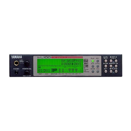
Page 4: Panel Layout
MU100 PANEL LAYOUT Front Panel A/D INPUT EFFECT button A/D INPUT level control EQ button PHONES jack MUTE / SOLO button POWER/VOL control ENTER button PLAY button EXIT button EDIT button PART buttons UTIL (UTILITY) button SELECT buttons MODE button... -
Page 5: Circuit Board Layout
MU100 CIRCUIT BOARD LAYOUT Front panel CN10 SW1 cable (10P) VR cable (10P) SW2 cable PSW cable (7P) (2P) LCD cable... -
Page 6: Block Diagram
MU100 BLOCK DIAGRAM... -
Page 7: Disassembly Procedure
MU100 DISASSEMBLY PROCEDURE Bottom Assembly 1-1 Remove the four (4) screws marked [60], the screw When you reattach the bottom assembly, you should marked [75], the screw marked [76] and the two (2) tighten the screws in the order described in figure 1. - Page 8 MU100 2-3 Remove the five (5) screws marked [T30]. The DM When you reattach the DM circuit board, you should circuit board can then be removed. (Fig. 3) tighten the screws in the order described in figure 3. Pull off the A/D INPUT knob from the DM circuit The cables plugged into the connector CN9 should board.
- Page 9 Be careful not to injure yourself when handling the jagged surfaces or sharp areas of the plug-in board. Instructions 1. Turn off the power of any devices that may be connected to the MU100 and remove the MU100’s AC adaptor from its power source.
- Page 10 5. Insert the expansion connector of the MU100 into the connector of the XG Plug-in Board. Make sure to insert the connector so that it faces the proper direction and the right and left tabs of the expansion connector lock into place (as shown in the illustration).
- Page 11 Side without the connector Screw (black) 7. Secure the DB cover back onto the MU100 by using the same four (4) silver screws that were removed in Step 2. Secure the screws in the order shown in the illustration. Screw (silver)
-
Page 12: Lsi Pin Description
Two Way Data Bus not used Analog Level Output L not used Detection of Host SW Position not used Battery Voltage Check ModelCheck (MU100:GND) Two Way Data Bus AVss LCD Data(DB7),SW Data,LED6 LCD Data(DB6),SW Strobe Data LCD Data(DB5),SW Strobe Data LCD Data(DB4),SW Data,LED5... - Page 13 MU100 TC203C760HF-001 (XR738A00) TC203C760HF-002 (XS725A00) SWP30 (AWM Tone Generator coped with MEG) Standard Wave Processor) NAME FUNCTION NAME FUNCTION (Ground) (Ground) HMD0 HMD1 HMD2 HMD3 HMD4 HMD5 Address bus internal register HMD6 HMD7 Wave memory data bus (Upper data memory)
-
Page 14: Ic Block Diagram
MU100 µPD63200GS-E1 (XP867A00) DAC (Digital to Analog Converter) NAME FUNCTION NAME FUNCTION 4/8F 4/8 Fs selection R. REF Channel R voltage reference D. GND Digital ground L. REF Channel L voltage reference 16 BIT 16 bit/18 bit selection L. OUT Channel L output D. - Page 15 MU100 MC34051MEL (XP881A00) TC74HC4066AF-T1 (XG385A00) SC7SU04FEL (XI348A00) NJU7660M-T1 (XP596A00) M5M34051FP (XV103A00) Quad Bilateral Analog Switch Inverter DC/DC Voltage Converter Dual EIA-422/423 Line Transceiver REC1 IN - IN/OUT 1 REC1 IN + DR1 IN OUT/IN 1 Control 1 VOLTAGE REC1 OUT...
-
Page 16: Circuit Boards
MU100 CIRCUIT BOARDS DM Circuit Board OUTPUT INPUT When removing MIDI THRU IN-A IN-B HOST TO HOST DC IN SELECT Lithium battery Push Battery holder When installing Lithium battery Battery holder Battery VN103500 VN103600(Battery holder for VN103500) Notice for back-up battery removal... - Page 17 MU100 PSW Circuit Board DM Circuit Board CN5: to DM-CN9 MUTE/ PLAY EDIT PART SOLO UTIL EFFECT ENITER SELECT MODE EQ EXIT VALUE Component side Pattern side PVR Circuit Board POWER/VOL PUSH ON/OFF to DM : CN 6 PHONES to DM : CN 13...
-
Page 18: Test Program
If an PB2 MEL Not using error is detected during the test, refer to section B, [EXIT] button. The MU100 will then wait for the entry of a 04 SWITCH & LED "PROCEEDING TROUGH THE TEST". test number. - Page 19 OK, the test will be completed and proceed to the next test. must be pulled out. The VOLUME control must be set at During the test, if the [EXIT] button is pressed, the MU100 maximum for this check. will wait for the entry of the test number.
- Page 20 Press the [ENTER] button. The MU100 will then A/D INPUT (L). automatically proceed to the next test. If the [EXIT] button is pressed, the MU100 will wait for TEST END the entry of the test number. Press the [ENTER] button. The MU100 will then 13.
- Page 21 When a sine wave signal of -11.5 dBm, 1 kHz is applied to If the [EXIT] button is pressed, the MU100 will wait for A/D INPUT (R), and A/D INPUT is set at minimum, and the entry of the test number.
- Page 22 OUTPUT (L,R). automatically proceed to the next test. If the [EXIT] button is pressed, the MU100 will wait for A signal is input from the AD input, goes through the DM the entry of the test number.
-
Page 23: Midi / Computer Connecting Cables
MU100 MIDI/COMPUTER CONNECTING CABLE MIDI Standard MIDI cable. Maximum length 15 meters. DIN 5-PIN DIN 5-PIN 2 (GND) Apple Macintosh Peripheral cable (M0197). Maximum length 2 meters. 2 (HSK i) MINI DIN MINI DIN 1 (HSK o) 8-PIN 8-PIN 5 (RxD –) 4 (GND) 3 (TxD –) -
Page 24: Error Messages
Illegal Data! A data error resulted during reception of MIDI messages. Try transmitting the data again, or turn the MU100 off and back on again. MIDI Buffer Full! Too much MIDI data is being received by the MU100 at one time. Reduce the amount of data being sent to the MU100. -
Page 25: Initialize
For the PFMInit setting, only the currently selected Performance will be initialized. For XGInit and GM Init, the initialized settings are the same as when the MU100 is reset upon receiving an XG System On or GM System On message. -
Page 26: Midi Implementation Chart
MU100 YAMAHA [ Tone Generator ] Date :27-JUL-1998 Model MU100 MIDI Implementation Chart Version : 1.1 Function... Transmitted Recognized Remarks Basic Default 1 - 16 Channel Changed 1 - 16 Default Mode Messages 3, 4 (m=1) Altered ************** Note 0 - 127... -
Page 27: Overall Circuit Diagram
MU100 OVERALL CIRCUIT DIAGRAM MU100 to LCD UNIT LCD UNIT LCD cable CONVERTER DC-DC MULTIPLEXER DA CONVERTER LINE TRANSCEIVER HSJ0912-01-010 OP AMP to HOST PHONES 10X2P 10X2P 21B0505 A10KX25W POWER/ HOST SELECT VOL. 3X2P CN14 to DM- CN13 INVERTER Photo Coupler... -
Page 28: Parts List
TONE GENERATOR PARTS LIST CONTENTS OVERALL ASSEMBLY ······························································································································································································ ELECTRICAL PARTS 4 ~ 11 ···················································································································································································· Notes : DESTINATION ABBREVIATIONS : Australian model M : South African model : British model O : Chinese model C : Canadian model Q : South-east Asia model D : German model : Taiwan model : European model... - Page 29 MU100 OVERALL ASSEMBLY Top assembly F140 F120 F130 F140 Front assembly F100 F110 Bottom assembly...
- Page 30 MU100 PART NO. DESCRIPTION REMARKS REF NO. RANK OVERALL ASSEMBLY MU100 J,U,E,W Front Assembly (VZ03500) Top Assembly (VZ03550) VR060800 Flat Head Tapping Screw-C 3.0X8 MFZN2BL VN103500 Lithium Battery CR2032 Bottom Assembly (VZ03510) EP600190 Bind Head Tapping Screw-B 3.0X8 MFZN2BL EG330360 Bind Head Screw 3.0X6 MFZN2BL...
-
Page 31: Electrical Parts
MU100 ELECTRICAL PARTS PART NO. DESCRIPTION REMARKS REF NO. RANK ELECTRICAL PARTS MU100 VZ018500 Circuit Board (XT466C0) VZ018400 Circuit Board (XT446C0) VZ018300 Circuit Board (XT446C0) VZ018500 Circuit Board (XT466C0) VZ018400 Circuit Board (XT446C0) VZ018300 Circuit Board (XT446C0) BAT1 VN103600 Battery Holder... - Page 32 MU100 PART NO. DESCRIPTION REMARKS REF NO. RANK UI566470 Electrolytic Cap. 4.70 50.0V UB013680 Monolithic Ceramic Cap. B 6800P 50V K UB052270 Monolithic Ceramic Cap. SL 270P 50V J UB013680 Monolithic Ceramic Cap. B 6800P 50V K UI566470 Electrolytic Cap.
- Page 33 MU100 PART NO. DESCRIPTION REMARKS REF NO. RANK UB012220 Monolithic Ceramic Cap. B 220P 50V K C151 C152 UJ838100 Electrolytic Cap. 100.00 16.0V C153 UB245100 Monolithic Ceramic Cap. F 0.100 25V Z C154 UB013470 Monolithic Ceramic Cap. B 4700P 50V K...
- Page 34 MU100 PART NO. DESCRIPTION REMARKS REF NO. RANK XQ138A00 NJM4556AMT1 IC22 OP AMP IC23 XF291A00 UPC4570G2 OP AMP XF291A00 UPC4570G2 OP AMP IC29 XS892A00 TLC320AD58CDWT-EL A/D Converter IC30 XS893A00 TL32088CNST-EL AD FRONT END IC31 XG385A00 TC74HC4066AF-T1 ANALOG SWITCH IC32 XH223A00...
- Page 35 MU100 PART NO. DESCRIPTION REMARKS REF NO. RANK Interchangeable VR243700 Chip Inductance (chip) 56U LEM2520 T 560J VQ464300 Chip Inductance (chip) NWL2520-560J Interchangeable VR243700 Chip Inductance (chip) 56U LEM2520 T 560J VL139800 Solid Inductance (chip) BLM31A700SPT 70ohm VL139800 Solid Inductance (chip)
- Page 36 MU100 PART NO. DESCRIPTION REMARKS REF NO. RANK RD154680 Carbon Resistor (chip) 68.0 1/4 J RD256680 Carbon Resistor (chip) 6.8K 0.1 J RD256680 Carbon Resistor (chip) 6.8K 0.1 J RD257120 Carbon Resistor (chip) 12.0K 0.1 J RD256100 Carbon Resistor (chip) 1.0K 0.1 J...
- Page 37 MU100 PART NO. DESCRIPTION REMARKS REF NO. RANK RD255470 Carbon Resistor (chip) 470.0 0.1 J -165 R166 RD257100 Carbon Resistor (chip) 10.0K 0.1 J -169 RD257100 Carbon Resistor (chip) 10.0K 0.1 J R170 RD256100 Carbon Resistor (chip) 1.0K 0.1 J...
- Page 38 MU100 PART NO. DESCRIPTION REMARKS REF NO. RANK VS609700 DM113Z-5BL3 VS276100 AC Adapter PA-5B VS353200 AC Adapter PA-5B VS353300 AC Adapter PA-5B New Parts RANK Japan only...