Table of Contents
Advertisement
RX-V4600/DSP-AX4600
This manual has been provided for the use of authorized YAMAHA Retailers and their service personnel.
It has been assumed that basic service procedures inherent to the industry, and more specifically YAMAHA Products, are already
known and understood by the users, and have therefore not been restated.
WARNING:
IMPORTANT:
The data provided is believed to be accurate and applicable to the unit(s) indicated on the cover. The research, engineering, and
service departments of YAMAHA are continually striving to improve YAMAHA products. Modifications are, therefore, inevitable
and specifications are subject to change without notice or obligation to retrofit. Should any discrepancy appear to exist, please
contact the distributor's Service Division.
WARNING:
IMPORTANT:
I CONTENTS
To Service Personnel .......................................... 2
Front Panels ............................................................ 3
Rear Panels .......................................................... 3~6
Remote Control ...................................................... 7
SPECIFICATIONS / 参考仕様 .................................. 8~10
Internal View ......................................................... 11
DISASSEMBLY PROCEDURES / 分解手順 .......... 12~15
ファームウェアの書き込み ..................................... 16~21
SELF DIAGNOSIS FUNCTION (DIAG) /
自己診断機能(ダイアグ) ..................................... 22~52
1 0 0 9 5 2
AV RECEIVER/AV AMPLIFIER
IMPORTANT NOTICE
Failure to follow appropriate service and safety procedures when servicing this product may result in personal
injury, destruction of expensive components, and failure of the product to perform as specified. For these reasons,
we advise all YAMAHA product owners that any service required should be performed by an authorized
YAMAHA Retailer or the appointed service representative.
The presentation or sale of this manual to any individual or firm does not constitute authorization, certification or
recognition of any applicable technical capabilities, or establish a principle-agent relationship of any form.
Static discharges can destroy expensive components. Discharge any static electricity your body may have
accumulated by grounding yourself to the ground buss in the unit (heavy gauge black wires connect to this buss).
Turn the unit OFF during disassembly and part replacement. Recheck all work before you apply power to the unit.
SERVICE MANUAL
AMP ADJUSTMENT / アンプ部調整 ........................... 53
Display Data ........................................................... 54
Ic Data ................................................................. 55~58
Block Diagram ................................................. 59~60
Pin Connection Diagram .............................. 61~62
Printed Circuit Board .................................. 63~83
Schematic Diagram ...................................... 85~100
Parts List ....................................................... 101~140
Remote Control .......................................... 141~143
2005
All rights reserved.
P.O.Box 1, Hamamatsu, Japan
'05.05
Advertisement
Table of Contents

Related Manuals for Yamaha RX-V4600/DSP


Summary of Contents for Yamaha RX-V4600/DSP
-
Page 1: Service Manual
This manual has been provided for the use of authorized YAMAHA Retailers and their service personnel. It has been assumed that basic service procedures inherent to the industry, and more specifically YAMAHA Products, are already known and understood by the users, and have therefore not been restated. -
Page 2: To Service Personnel
RX-V4600/DSP-AX4600 I TO SERVICE PERSONNEL AC LEAKAGE WALL EQUIPMENT TESTER OR 1. Critical Components Information OUTLET UNDER TEST EQUIVALENT Components having special characteristics are marked s and must be replaced with parts having specifications equal to those originally installed. 2. Leakage Current Measurement (For 120V Models Only) -
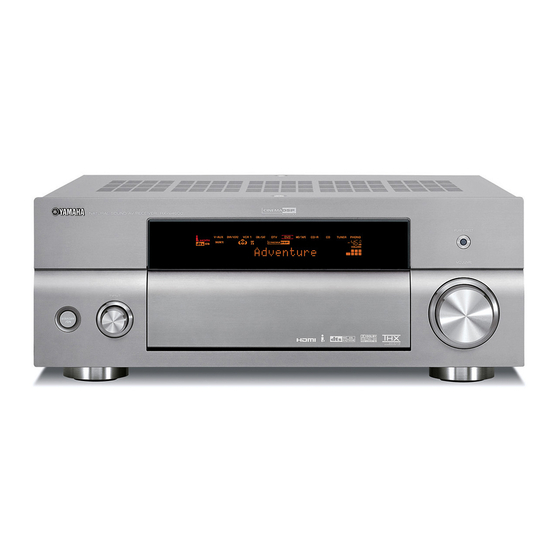
Page 3: Front Panels
RX-V4600/DSP-AX4600 I FRONT PANELS RX-V4600 (U, C, R, T, K, A, B, G, L models) DSP-AX4600 (J model) I REAR PANELS RX-V4600 (U model) - Page 4 RX-V4600/DSP-AX4600 RX-V4600 (C model) RX-V4600 (R model) RX-V4600 (T model)
- Page 5 RX-V4600/DSP-AX4600 RX-V4600 (K model) RX-V4600 (A model) RX-V4600 (B model)
- Page 6 RX-V4600/DSP-AX4600 RX-V4600 (G model) RX-V4600 (L model) DSP-AX4600 (J model)
-
Page 7: Remote Control
RX-V4600/DSP-AX4600 I REMOTE CONTROL RX-V4600 (U, C, R, T, K, A, L models) RX-V4600 (B, G models) DSP-AX4600 (J model) RX-V4600 (U model) RX-V4600 (C, R, T, K, A, B, G, L models) -
Page 8: Specifications
RX-V4600/DSP-AX4600 I SPECIFICATIONS / 参考仕様 I Audio Section / オーディオ部 Minimum RMS Output Power (Power Amp. Section) / 定格出力 (パ Tone Control Characteristics / トーンコントロール特性 ワーアンプ部) (20 Hz to 20 kHz) BASS Boost/Cut ..............±6dB (50Hz) FRONT L/R U, C, R, T, K, A, B, G, L models (0.04% THD, 8 ohms) ..130W + 130W Turnover Frequency ............ - Page 9 “Dolby”, “Surround EX”, and the double-D symbol are trademarks of Dolby Laboratories. ドルビーラボラトリーズからの実施権に基づき製造されています。 「ドルビー」 、 「PRO LOGIC」 、 「Surround EX」 およびダブルD記号 は、ドルビーラボラトリーズの商標です。 “SILENT CINEMA” is a trademark of YAMAHA CORPORATION. 「サイレントシネマ/SILENT CINEMA」 はヤマハ株式会社の登録商標 です。 HD Radio technology manufactured under license from iBiquity Digital Corporation.
- Page 10 RX-V4600/DSP-AX4600 • SET MENU TABLE / セットメニュー AUTO SETUP MAIN MENU PARAMETER SETUP AUTO FLAT / FRONT / [NATURAL] START PUSH + MANUAL SETUP MAIN MENU SUB MENU PARAMETER SETTING VALUE ([ ] INITIAL VALUE) MAIN MENU SUB MENU PARAMETER...
-
Page 11: Internal View
RX-V4600/DSP-AX4600 I INTERNAL VIEW RX-V4600 (U, C, R, T, K, A, B, G, L models) POWER (5) P.C.B. 2 3 4 5 6 7 8 9 0 A B POWER (4) P.C.B. (R, L models) MAIN (1) P.C.B. MAIN (5) P.C.B. -
Page 12: Disassembly Procedures
RX-V4600/DSP-AX4600 I DISASSEMBLY PROCEDURES / 分解手順 (番号順に部品を取り外してください。) (Remove parts in the order as numbered.) Disconnect the power cable from the AC outlet. AC電源コンセントから、電源コードを抜いてください。 1. トップカバーの外し方 1. Removal of Top Cover a. 1 のネジ2本、 2 のネジ4本、 3 のネジ5本を外しま a. Remove 2 screws (1), 4 screws (2) and 5 screws (3). - Page 13 RX-V4600/DSP-AX4600 5. Removal of FUNCTION (3) P.C.B. 5. FUNCTION (3) P.C.B.の外し方 U, C, R, T, K, A, B, G, L models a. C のネジ1本を外し、サポートトップを外します。 (Fig. a. Remove 1 screw (C) and then remove the Support Top. (Fig. 2) 2) b. D のネジ1本を外します。 (Fig. 3)...
- Page 14 RX-V4600/DSP-AX4600 7. Removal of Fan 7. ファンの外し方 When checking the P.C.B.: P.C.B.チェックをする場合には a. G のプッシュリベット4本を外し、カバーを外します。 a. Remove 4 push rivets (G) and then remove the Cover. ・ 本機の上にゴムシートと布を敷き、その上にP.C.B.を • Put the Rubber Sheet and a Cloth over the equipment. (Fig. 5) (Fig.
- Page 15 RX-V4600/DSP-AX4600 When checking the Amp Unit: アンプユニットをチェックする場合には ・ アンプユニットはヒートシンクといっしょに、アート • Put the Amp Unit together with the heat sink upright ベースの上に立ててチェックします。 (Fig. C) on the art base and check them. (Fig. C) • Reconnect all cables (connectors) that have been ・...
-
Page 16: Updating Firmware
RX-V4600/DSP-AX4600 I UPDATING FIRMWARE / ファームウェアの書き込み 下記のサービス部品を交換した場合、ファームウェアの書 After replacing the following service parts, be sure to perform writing of the firmware. き込みを行ってください。 •CONTROL P.C.B. ・CONTROL P.C.B. ・IC503 (CONTROL P.C.B.) •IC503 (CONTROL P.C.B.) •DUAL P.C.B. ・DUAL P.C.B. ・IC318 (DUAL P.C.B.) •IC318 (DUAL P.C.B.) Make sure to use the following procedure for firmware ファームウェアを書き込む場合は、必ず下記の手順で行っ... - Page 17 RX-V4600/DSP-AX4600 b. DSP FLASHER を実行します。(Fig. 2) b. Execute DSP FLASHER. (Fig. 2) c. Select the COM port to use and press the [connect] c. 使用COMポートを選択し [connect] ボタンを押します。 button, and the Com Port Status changes to Com Port Status が “connected” に変わります。(Fig. 3) "connected".
- Page 18 RX-V4600/DSP-AX4600 f. 本体の “SPEAKERS A” キーを押しながら “PROGRAM” f. While pressing the "SPEAKERS A" key of the main unit, turn the "PROGRAM" knob until "Upgrade Main" is ツマミを回し “Upgrade Main” をディスプレイに表示させ displayed. (Fig. 6) ます。 (Fig. 6) Fig. 6 g. 本体の “MULTI CH INPUT” キーを押しながら “STRAIGHT/ g.
- Page 19 RX-V4600/DSP-AX4600 h. 書き込むファームウェアのファイルをドラッグアンドド h. Drag and drop the file of the firmware to be written or select the file using the [OPEN] button. (Fig. 9) ロップするか、 [OPEN] ボタンでファイルを選択します。 (Fig. 9) Fig. 9 i. Pressing the [EPS] button will start writing. (Fig. 10) i.
- Page 20 RX-V4600/DSP-AX4600 k. DSP FLASHER の [EXIT] ボタンを押して終了します。 k. Press the [EXIT] button of DSP FLASHER. This completes the writing procedure. (Fig. 12) (Fig. 12) * Perform "Step.2 Writing of HDMI" without turning off ※ 本体の電源は切らずに “Step.2 HDMIの書き込み” を行 the power to the main unit.
- Page 21 RX-V4600/DSP-AX4600 Fig. 13 Fig. 14 * If writing is not successful or the power cannot be ※ 書き込みの途中で失敗したり、書き込み終了後に電源が turned on after writing, it is possible to enter the 入らない場合、 「強制BOOTモード」 で書き込みモードに 入ることができ、再度書き込みを行うことができます。 updating mode by using "FORCED BOOT MODE" and execute writing again.
- Page 22 RX-V4600/DSP-AX4600 I SELF DIAGNOSIS FUNCTION (DIAG)/自己診断機能 (ダイアグ) There are 26 DIAG menu items, each of which has sub- ダイアグメニューは2 6 個あり、そのそれぞれにサブメ ニューがあります。下表はメニュー一覧です。 menu items. Listed in the table below are menu items and sub-menu items. No DIAG MENU SUB MENU DA60Y-YSS930 1.
- Page 23 RX-V4600/DSP-AX4600 No DIAG MENU SUB MENU 12 AD DATA CHECK / FAN TEST 1. PS (protection) 2. DC (protection) / FAN OUT 3. TH 4. REC-OUT 5. PL 6. K0 / K1 (panel key) 7. FAN DRIVE TEST: HIGH (Fan test only applies to models with a fan. / ファン装備モデルに適用...
- Page 24 RX-V4600/DSP-AX4600 No DIAG MENU SUB MENU 22 1394 CONNECT 1. 1394 NONE : No Connect 2. 1394 IN 1 : 1st Device (Lower GUID) 3. 1394 IN 2 : 2nd Device (Middle GUID) 4. 1394 IN 3 : 3rd Device (Upper GUID) 23 INPUT MODE 1.
- Page 25 RX-V4600/DSP-AX4600 • Starting DIAG ● ダイアグの起動 Press the “STANDBY/ON” key while simultaneously 本体の下図に示すキーを同時に押しながら “STANDBY/ pressing those two keys of the main unit as indicated in the ON” キーを押すと、ダイアグが起動します。 figure below. / 本体キー Keys of main unit Turn on the power while pressing these keys.
- Page 26 RX-V4600/DSP-AX4600 • Display provided when DIAG started ● ダイアグ起動時の表示 The FL display of the main unit displays the protection 本体のFLディスプレイにプロテクション履歴情報とバー ジョン (英1文字) が表示され、数秒後にダイアグメニュー function history data and the version (1 alphabet) and the (No.1 DSP THROUGHのサブメニューYSS 0dB) になりま DIAG menu [sub-menu (YSS 0dB) of DIAG menu No.1 DSP THROUGH] a few seconds later.
- Page 27 RX-V4600/DSP-AX4600 When there is a history of protection function due to abnormal voltage in the power supply section Version (1 alphabet) 電源部の電圧異常によるプロテク バージョン (英1文字) ション履歴がある場合 Voltage display in % 電圧の%表示 Cause: The voltage in the power supply section is 原因: 電源部の電圧が異常。...
- Page 28 RX-V4600/DSP-AX4600 • History of protection function ● プロテクションの履歴 When the protection function has worked, its history is プロテクションが働いた場合、履歴をバックアップして stored in memory with a backup. Even if no abnormality 記憶しています。サービスのときに異常が認められなく is noted while servicing the unit, an abnormality which ても、バックアップが残っていれば、お客様のところで has occurred previously can be defined as long as the 起きた異常を区別できます。...
- Page 29 RX-V4600/DSP-AX4600 • Functions in DIAG mode ● ダイアグ中の機能 In addition to the DIAG menu items, functions as listed ダイアグメニューの他に、以下の機能が動作します。 below are available. ・インプット切り換え、マルチチャンネルインプット • Input selection, Multi channel input ・センター、リア、リアセンター、サブウーファーレベル • Center/Rear/Rear center/Sub-woofer level adjustment 調整 • Muting ・ミューティング • Speaker relay A/B ・スピーカーリレーA/B...
- Page 30 RX-V4600/DSP-AX4600 • Details of DIAG menu ● ダイアグメニュー詳細 With full-bit output specified in some modes, it is possible 一部のモードでフルビット指定することで、各チャンネル to execute 0dBFS output without head margin in each のヘッドマージンを廃して0dBFS出力することが可能で channel. す。 1. DA60Y-YSS930 1. DA60Y-YSS930 This function is for YSS930 only. Main DSP of YSS930 YSS930のみの動作です。FRONT出力にはYSS930の...
- Page 31 RX-V4600/DSP-AX4600 2. BYPASS 2. BYPASS ANALOG BYPASS ANALOG BYPASS Reference data INPUT: DVD ANALOG SUBWOOFER OUTPUT: 50Hz, Others: 1kHz SPEAKER OUT SUBWOOFER Input level Volume FRONT CENTER SURROUND SURROUND BACK PRESENCE OUTPUT - ∞ - ∞ - ∞ - ∞...
- Page 32 RX-V4600/DSP-AX4600 3. RAM THROUGH 3. RAM THROUGH Using the sub-menu, it is possible to select the full-bit サブメニューにより出力レベル0dB、フルビット出力が output at 0dB output level. 選択可能です。 RAM 0dB RAM 0dB Reference data INPUT: DVD ANALOG SUBWOOFER OUTPUT: 50Hz, Others: 1kHz SPEAKER OUT...
- Page 33 RX-V4600/DSP-AX4600 4. PRO LOGIC / NEO6 4. PRO LOGIC / NEO6 PRO LOGIC I PRO LOGIC I Reference data INPUT: DVD ANALOG SUBWOOFER OUTPUT: 50Hz, Others: 1kHz SPEAKER OUT SUBWOOFER Input level Volume FRONT CENTER SURROUND SURROUND BACK PRESENCE OUTPUT - ∞...
- Page 34 RX-V4600/DSP-AX4600 5. SPEAKERS SET 5. SPEAKERS SET The input signal is automatically identified in the order 入力は、dts→ DOLBY DIGITAL → AAC → PCM → ア of dts → DOLBY DIGITAL → AAC→ PCM → Analog. ナログの優先順で自動判別されます。 There are seven sub-menu items as follows. The サブメニューは以下の7つあります。...
- Page 35 RX-V4600/DSP-AX4600 6. EXTERNAL INPUT 6. EXTERNAL INPUT It is possible to select the 6ch/8ch input and 6_/8_ by サブメニューにより、6ch/8ch入力および6Ω/8Ωが選択 using the SUB menu. 可能です。 6CH INPUT_6OHMS 6CH INPUT_6OHMS 6CH INPUT_8OHMS 6CH INPUT_8OHMS 8CH INPUT_6OHMS 8CH INPUT_6OHMS 8CH INPUT_8OHMS 8CH INPUT_8OHMS...
- Page 36 RX-V4600/DSP-AX4600 8. EFFECT OFF / DISPLAY CHECK 8. EFFECT OFF / DISPLAY CHECK Use this program to check the FL display section and FL表示部と映像制御部のチェックプログラムです。 映 image control section. When checking the image 像制御部をチェックする場合には、モニター、コンポー ネントビデオケーブル、Sビデオケーブル、ビデオ用ピ control section, prepare a monitor, component video cable, S video cable and video pin cable and connect ンケーブルを準備し、接続します。...
- Page 37 RX-V4600/DSP-AX4600 Check of the Video control circuit. (Monitor out) / 映像表示部のチェック(モニター出力) The image signal is output as follows. 映像信号は以下のように出力されます。 Initial display/Video conversion OFF INPUT OUTPUT 初期表示/ビデオコンバージョンOFF (D4 VIDEO JACK) (D4 VIDEO JACK) J model only J model only (D4ビデオ端子) (D4ビデオ端子)...
- Page 38 RX-V4600/DSP-AX4600 9. MANUAL TEST 9. MANUAL TEST DSP内蔵のノイズ発生回路によって、サブメニューで指 The noise generator with a built-in DSP outputs the test 定したチャンネルへテストノイズを出力します。 noise through the channels specified by the sub-menu. LFE用のノイズ周波数は35∼250Hz、それ以外は中心周 The noise frequency for LFE is 35 to 250 Hz. Other than that, the center frequency is 800Hz.
- Page 39 RX-V4600/DSP-AX4600 11. FACTORY PRESET 11. FACTORY PRESET This menu is used to reserve and inhibit initialization of バックアップ用RAM (音場プログラムのパラメーターや the back-up RAM. The signals are processed using セットメニュー内容等) の初期化を予約/禁止します。 信号処理はEFFECT OFFと同じです (ANALOG MAIN EFFECT OFF. (The L/R signal is output using ANALOG MAIN BYPASS.)
- Page 40 RX-V4600/DSP-AX4600 12. AD DATA CHECK / FAN TEST 12. AD DATA CHECK / FAN TEST This menu is used to display the A/D conversion value 本体パネルキー、プロテクションなどを検出しているメ of the main CPU which detects panel keys of the main インCPUのA/D変換の値を、サブメニューで%表示しま す。信号処理は実行前の状態を維持します。 unit and protection functions in % using the sub-menu.
- Page 41 RX-V4600/DSP-AX4600 POWER LIMIT (パワーリミッターの検出) POWER LIMIT (Power limiter detection) PL: Power limiter detection value PL: パワーリミッター検出の値 The voltage value of pin No. 135 of IC520 is displayed, IC520 135ピンの電圧値を5V/256を基準にして表示し ます。 using 5V/256 as standard. Based on the input voltage value of pin No.135 of IC520 135ピンの入力電圧値により、IC505の6ピン...
- Page 42 RX-V4600/DSP-AX4600 13. V CONV STATUS 13. V CONV STATUS The data received from the video conversion IC ビデオコンバージョンIC (TA1270) からの受信データを (TA1270) is displayed. 表示します。 LOW BYTE DATA LOW BYTE DATA The status information of TA1270 is displayed in the TA1270のステータス情報を2進数で表示します。...
- Page 43 RX-V4600/DSP-AX4600 14. IF STATUS 14. IF STATUS (Input function status) Using the sub-menu, the status data is displayed one サブメニュー操作により、以下のステータス情報を順次 after another in the hexadecimal notation. 16進数で表示します。信号処理は、本メニュー実行前 の状態を維持します。 During signal processing, the status before execution of this menu is maintained.
- Page 44 RX-V4600/DSP-AX4600 <第5バイト>信号処理ステータス情報 <5th byte> Signal processing status information *2: With digital signals other than 32kHz, 44.1kHz and *2: 32kHz、44.1kHz、48kHz以外のデジタル信号の場 48kHz, through processing method is used for 合、再生可能な信号についてはスルー処理されます。 reproducible signals. bit7 MUTE request bit3 – bit6 Red dts flashing bit2 Through & bypass (*2) bit5 6.1/EX processing...
- Page 45 RX-V4600/DSP-AX4600 15. DSP RAM CHECK 15. DSP RAM CHECK This menu is used to self-diagnose whether or not the YSS930と外付けRAMとのバス接続の正否を自己診断し bus connection for the YSS930 and the external RAM is ます。 信号処理は、このメニューを実行する前の状態を維持し made properly. During signal processing, the status before execution ます。...
- Page 46 RX-V4600/DSP-AX4600 17. SOFT SW 17. SOFT SW This menu is used to switch the function settings on P.C.B.上の機能設定をソフト的に切り替えて、製品を動 P.C.B. through the software so as to activate the 作させる機能です。 プロテクション機能は、P.C.B.の設定に従います。AC product. The protection function follows the P.C.B. settings. 接続またはメーカープリセットで、P.C.B.の設定に初期 化されます。初期化後の各機能の表示は、P.C.B.上の設 When connected to AC or in the maker preset state, the 定によります。操作は、サブメニューを選んだ後、...
- Page 47 HDMI Vendor Name HDMI Vendor Name The vendor name (YAMAHA) of this unit written in the D M I モ ジ ュ ー ル に 書 き 込 ま れ て い る 本 機 の ベ ン ダ 名...
- Page 48 RX-V4600/DSP-AX4600 20. PCB SELF CHECK 20. PCB SELF CHECK HDMI SELF CHECK HDMI SELF CHECK HDMIモジュールの自己診断結果を読み出して表示しま The self-diagnosis result of HDMI module is read and displayed. す。 表示 判断 Display Description NoEr No error detected. NoEr 不良検出なし NoChck No check NoChck 未検出...
- Page 49 RX-V4600/DSP-AX4600 22. 1394 CONNECT 22. 1394 CONNECT 1394 NONE : No Connect 1394 NONE : No Connect i.LINK 1端子とi.LINK 2端子のどちらも入力セレクトしませ Neither i.LINK 1 terminal nor i.LINK 2 terminal is selected for input. ん。 1394 IN 1 : 1st Device (Lower GUID) 1394 IN 1 : 1st Device (Lower GUID) With i.LINK device connected to i.LINK 1 terminal or...
- Page 50 RX-V4600/DSP-AX4600 23. INPUT MODE 23. INPUT MODE SPDIF Fix SPDIF Fix 信号経路をSPDIFにします。 Select SPDIF for the signal passage. 1394 I2S 1394 I2S Select I2S of 1394 module for the signal passage. 信号経路を1394モジュールのI2Sにします。 HDMI I2S HDMI I2S 信号経路をHDMIモジュールのI2Sにします。 Select I2S of HDMI module for the signal passage.
- Page 51 RX-V4600/DSP-AX4600 25. F/W INFO 25. F/W INFO HDMI Firmware Version HDMI Firmware Version HDMIファームウェアのバージョンを表示します。 Displays the version of HDMI firmware. HDMI Firmware CheckSum HDMI Firmware CheckSum Displays the checksum of HDMI firmware. HDMIファームウェアのチェックサムを表示します。 1394 Firmware Version 1394 Firmware Version 1394ファームウェアのバージョンを表示します。...
- Page 52 RX-V4600/DSP-AX4600 26. マイコン情報 26. MICROPROCESSOR INFORMATION The version, checksum and the port specified by the サブメニューは7つあります。 microprocessor are displayed. The signal is processed プログラムのバージョン、チェックサム、マイコンの指 定ポートを表示します。 using EFFECT OFF. The checksum is obtained by adding the data at every 16 bits for each program area 信号はエフェクトOFFです。チェックサムは、プログラ...
-
Page 53: Amp Adjustment
RX-V4600/DSP-AX4600 I AMP ADJUSTMENT / アンプ部調整 アンプユニットのアイドリング電流の確認 Confirmation of Idling Current of Amp ● 電源投入直後、R319 (MAIN Lch) 、R320 (MAIN REAR Unit Rch) 、R325 (CENTER) 、R326 (SURROUND • Right after power is turned on, confirm that the voltage Lch) 、R327 (SURROUND Rch) 、R321 MAIN (2) P. -
Page 54: Display Data
RX-V4600/DSP-AX4600 I DISPLAY DATA G V901 : HNA-17ML01T (WF098500) G ANODE CONNECTION 14G~2G PATTERN AREA G PIN CONNECTION Pin No. Connection Pin No. Connection Note : 1) F1, F2 ..Filament 2) NP ..No pin 3) NC ..No connection 4) 1G ~ 17G .. - Page 55 RX-V4600/DSP-AX4600 IC501 : M30805SGP (CONTROL P.C.B) I IC DATA 16bit µ-COM (Main CPU) IC501 : M30805SGP (CONTROL P.C.B) Port Name Terminal Name Function 16bit µ-COM (Main CPU) PowerOn Standby MCUSleep [AC OFF] TXDH TXD4 Transmission HDMI data CLKH CLK4 Transmission HDMI clock...
- Page 56 RX-V4600/DSP-AX4600 IC501 : M30805SGP (CONTROL P.C.B) IC501 : M30805SGP (CONTROL P.C.B) 16bit µ-COM (Main CPU) 16bit µ-COM (Main CPU) Port Name Terminal Name Function Port Name Terminal Name Function PowerOn Standby MCUSleep [AC OFF] PowerOn Standby MCUSleep [AC OFF] SCKN...
- Page 57 RX-V4600/DSP-AX4600 IC512: D60YA003BPYP225 (DSP P.C.B) IC512: D60YA003BPYP225 (DSP P.C.B) Decoder Decoder * No service part No. Name Function Digital Signal Processors avilable. 41 SCL0 I2C0 clock EMIF32 L2 Cache/ L1P Cache Memory ※ サービス部品として供給し Direct Mapped 42 SDA0 I2C0 data...
- Page 58 RX-V4600/DSP-AX4600 IC512: D60YA003BPYP225 (DSP P.C.B) IC512: D60YA003BPYP225 (DSP P.C.B) Decoder Decoder No. Name Function No. Name Function 157 CVDD 1.2V power supply 99 EA17 For external memory, Address 17 (Unconnected) 158 VSS Ground 100 EA19 For external memory, Address 19 (Unconnected)
- Page 59 RX-V4600/DSP-AX4600 I BLOCK DIAGRAM (1/2) DSD3 i.LINK MPCM DSD4 DSD5 DSD0 MAIN IC531 DSD1 • See page 91 → SCHEMATIC DIAGRAM DSD2 IC536 MPCM HDMI DUAL DSDSL POWER • See page 85, 86 → SCHEMATIC DIAGRAM • See page 92 → SCHEMATIC DIAGRAM DSDSR •...
- Page 60 RX-V4600/DSP-AX4600 I BLOCK DIAGRAM (2/2) IC309 HDMI DUAL RECEIVER HDMI IC308 HDMI TRANSMITTER DUAL • See page 97, 98, 99 → SCHEMATIC DIAGRAM INPUT • See page 93, 94 → SCHEMATIC DIAGRAM INHIBIT INHIBIT IC702 Composite IC701 Source INPUT • See page 93, 94 → SCHEMATIC DIAGRAM...
- Page 61 RX-V4600/DSP-AX4600 I PIN CONNECTION DIAGRAM • ICs µPC29M33T-E1 µPC2905AT LM61CIZ NJM7805FA NJM79M05FA RH5RE39AA PQ012FZ01ZP PQ03RD23 PQ09RF11 PQ1CG2032FZ NJM7812FA NJM79M12FA PQ025EZ5MZPH PQ05RD21 µPC2933AT RH5RE58AA NJM7809FA µPC37M31TJ-E1 PQ05RD11 4:GND 3: IN 1:IN 1: OUTPUT 3: GND 3: IN 3: COM 2:GND 2: COM...
- Page 62 RX-V4600/DSP-AX4600 • Diodes 1N4002S MTZJ3.0A 1SS355 1SS133 MTZJ3.0B 1SS380 Anode 1SS244 MTZJ33B MA8051-M Anode MTZJ4.7C MA8051-L MTZJ5.1B MA8056-M MTZJ6.8B MA8068-L Cathode MTZJ7.5C RB501V-40 MTZJ10B Cathode UDZ3.6BTE-17 MTZJ24C UDZ5.1B RB441Q-40 UDZS5.6BTE-17 RB051L-40 D2SBA20 D15XB20 S1NB20 D3SBA20 S1NB60 – – – • Transistors...
- Page 63 RX-V4600/DSP-AX4600 I PRINTED CIRCUIT BOARD (Foil side) • Semiconductor Location Ref. No. Location D501 D509 CONTROL DUAL (CB5) IC501 (CB511) DUAL IC502 (CB302) OPERATION (3) IC504 POWER (3) DSP P.C.B. (Side A) Lead Solder Used IC505 (CB905) (W127) IC506 IC507...
- Page 64 RX-V4600/DSP-AX4600 I PRINTED CIRCUIT BOARD (Foil side) • Semiconductor Location Ref. No. Location D502 D503 D504 DSP P.C.B. (Side B) Lead Free Solder Used D508 D701 D702 D703 D704 D705 D706...
- Page 65 RX-V4600/DSP-AX4600 I PRINTED CIRCUIT BOARD (Foil side) FUNCTION (3) FUNCTION (1) P.C.B. (CB523) FUNCTION (1) P.C.B. (Side B) Lead Free Solder Used (Side A) Lead Solder Used RS-232C FRONT /ICEV CEEV SURROUND DTEV PRE OUT DTEV3 CKEV CENTER/ SCKA SDATA...
- Page 66 RX-V4600/DSP-AX4600 I PRINTED CIRCUIT BOARD (Foil side) FUNCTION (2) P.C.B. (Side A) Lead Solder Used FUNCTION (2) P.C.B. (Side B) Lead Free Solder Used FUNCTION (3) (CB533) CONTROL (CB509) RDATA RCLK /ICEV CEEV DTEV CKEV SDATA SCKA ATTF MTZ3 MTZ2...
- Page 67 RX-V4600/DSP-AX4600 I PRINTED CIRCUIT BOARD (Foil side) • Semiconductor Location Ref. No. Location D508 D509 D510 FUNCTION (3) P.C.B. (Side A) Lead Solder Used IC550 Q515 Q516 Q517 Q547 /VMT /Z2VMT INPUT (2) SDTN RCLK SCKN RDATA FUNCION (2) (CB702)
- Page 68 RX-V4600/DSP-AX4600 I PRINTED CIRCUIT BOARD (Foil side) FUNCTION (3) P.C.B. (Side B) Lead Free Solder Used Circuit No. R, T, K, A, L B, G C582, 583, 586, 587 C588, 589, 609, 610 C611-614 C615, 623 C616-619 C620, 624 C621, 622...
- Page 69 RX-V4600/DSP-AX4600 I PRINTED CIRCUIT BOARD (Foil side) FUNCTION (4) P.C.B. (Side A) Lead Solder Used FUNCTION (1) FUNCTION (5) P.C.B. FUNCTION (6) P.C.B. (CB510) (Side A) Lead Solder Used (Side A) Lead Solder Used INPUT (2) (CB703) FUNCTION (2) FUNCTION (2)
- Page 70 RX-V4600/DSP-AX4600 I PRINTED CIRCUIT BOARD (Foil side) • Semiconductor Location Ref. No. Location D901 OPERATION (1) P.C.B. (Side A) OPERATION (6) P.C.B. (Side A) D902 D905 CONTROL D909 (CB508) D910 D911 OPERATION (8) D912 (CB461) D913 D914 D915 STANDBY IC901...
- Page 71 RX-V4600/DSP-AX4600 I PRINTED CIRCUIT BOARD (Foil side) • Semiconductor Location Ref. No. Location D906 D903 IC902 OPERATION (2) P.C.B. (Side A) OPERATION (7) P.C.B. (Side A) OPERATION (3) P.C.B. (Side A) IC904 Q901 OPERATION (4) VOLUME +5SPC CONTROL (W902B) CONTROL...
- Page 72 RX-V4600/DSP-AX4600 I PRINTED CIRCUIT BOARD (Foil side) OPERATION (4) P.C.B. (Side A) REC OUT MAIN (1) (W220) OPERATION (5) P.C.B. (Side A) +5SPC OPERATION (3) (W902A) +5M2 PLMT PRIO TRG2 LIMIT TRG1 RM3+ +5M2 RM3- RM2+ THM1 RM2- THM2 OPERATION (4) P.C.B. (Side B) Lead Free Solder Used...
- Page 73 RX-V4600/DSP-AX4600 I PRINTED CIRCUIT BOARD (Foil side) • Semiconductor Location Ref. No. Location D460 D461 D462 D463 D464 IC460 IC461 IC462 IC464 OPERATION (8) P.C.B. (Side A) OPERATION (8) P.C.B. (Side B) Lead Free Solder Used IBOC (CB3) (U model)
- Page 74 RX-V4600/DSP-AX4600 I PRINTED CIRCUIT BOARD (Foil side) Lead Free Solder Used MAIN (1) P.C.B. (Side A) SURROUND / SURROUND BACK – – PRESENCE / ZONE 2 MAIN (2) P.C.B. (Side A) (W207A) MAIN (4) (W206A) SPA+ MAIN (3) SPA- SPB+...
- Page 75 RX-V4600/DSP-AX4600 I PRINTED CIRCUIT BOARD (Foil side) • Semiconductor Location Lead Free Solder Used Ref. No. Location D209 D210 D211 MAIN (3) P.C.B. (Side A) MAIN (5) P.C.B. (Side A) D212 D213 D216 D217 FRONT A/B CENTER D218 D219 –...
- Page 76 RX-V4600/DSP-AX4600 I PRINTED CIRCUIT BOARD (Foil side) • Semiconductor Location Lead Free Solder Used Ref. No. Location POWER (1) P.C.B. POWER (4) P.C.B. (Side A) OPERATION (5) (CB549) (Side A) R, L models FUNCTION (1) (W501) Power Transformer Power Transformer...
- Page 77 RX-V4600/DSP-AX4600 I PRINTED CIRCUIT BOARD (Foil side) • Semiconductor Location Lead Free Solder Used Ref. No. Location POWER (5) P.C.B. (Side A) POWER (6) P.C.B. (Side A) MAIN (3) FUNCTION (1) (W505) (W218) AC IN FAN- Flock FAN+ /RES PDET...
- Page 78 RX-V4600/DSP-AX4600 I PRINTED CIRCUIT BOARD (Foil side) INPUT (1) P.C.B. (Side A) Lead Solder Used INPUT (1) P.C.B. (Side B) Lead Free Solder Used CONTROL FUNCTION (5) FUNCTION (5) (CB515) (CB522) (CB521) FUNCTION (4) (CB548) ATTF SCKA SDTA RDATA RCLK (CB506) •...
- Page 79 RX-V4600/DSP-AX4600 I PRINTED CIRCUIT BOARD (Foil side) INPUT (2) P.C.B. (Side A) Lead Solder Used INPUT (2) P.C.B. (Side B) Lead Free Solder Used VIDEO DVR/ VCR 1 VCR 2 ZONE2 MONITOR CBL/SAT /VMT /Z2VMT SDTN SCKN CMP0 CMP1 SEP_Y...
- Page 80 RX-V4600/DSP-AX4600 I PRINTED CIRCUIT BOARD (Foil side) CONTROL P.C.B. (Side A) Lead Solder Used OPERATION (1) FUNCTION (3) (CB904) (CB505) (CB539) POWER (5) POWER (3) (W1) DUAL FUNCTION (3) (W124) (CB303) (CB538) J model DVD A C716 D4 VIDEO KEY1B...
- Page 81 RX-V4600/DSP-AX4600 I PRINTED CIRCUIT BOARD (Foil side) • Semiconductor Location Ref. No. Location Ref. No. Location Ref. No. Location Ref. No. Location Ref. No. Location Ref. No. Location Ref. No. Location Ref. No. Location D501 D512 D754 D761 Q511 Q518...
- Page 82 RX-V4600/DSP-AX4600 I PRINTED CIRCUIT BOARD (Foil side) DUAL P.C.B. (Side A) Lead Solder Used DUAL P.C.B. (Side B) Lead Free Solder Used i.LINK (AUDIO) HDMI S400 IN 1 IN 2 OPERATION(8) (CB468) • Semiconductor Location Ref. No. Location Ref. No. Location Ref. No. Location Ref.
- Page 83 RX-V4600/DSP-AX4600 I PRINTED CIRCUIT BOARD (Foil side) • Semiconductor Location IBOC MODULE Ref. No. Location IBOC P.C.B. (Side A) Lead Solder Used U model TUNER PACK TUNER OPERATION(8) (CB470) IBOC P.C.B. (Side B) Lead Free Solder Used FUNCTION(3) (CB534) U model...
- Page 84 RX-V4600/DSP-AX4600 MEMO MEMO...
- Page 85 RX-V4600/DSP-AX4600 SCHEMATIC DIAGRAM (DSP 1/2) Page 89 to OPERATION(3) – V-AUX – CB905 Page 98 Page 92 Page 95 IC511: SN74AHCT08PWR IC510: SN74AHCT1G32DCKR to POWER(3)_W127 to CONTROL_CB511_23Pin to DUAL_HDMI_CB302 Quad 2-Input And Gate 2-Input or Gate IC513: SN74LV245APWR Octal Bus Transceiver with 3-state Outputs...
- Page 86 RX-V4600/DSP-AX4600 SCHEMATIC DIAGRAM (DSP 2/2) Page 95 Page 93 to CONTROL (AUDIO)_CB502_19Pin to INPUT_W301 FRONT L IC516, 518: YSS930-SZ 11.7 3. 9 MICROPROCESSOR 3. 9 3. 9 INTERFACE PROGRAM COEFFICIENT ADDRESS CONTROL REGISTER 50 bit *1024 word 16 bit *1024 word 17 bit *256 word...
- Page 87 RX-V4600/DSP-AX4600 SCHEMATIC DIAGRAM (FUNCTION 1/2) Page 88 Page 88 to FUNCTION (3) – C-F_CNCT – CB533 to FUNCTION (3) – C-F_CNCT – CB523 IC529: YAC523-EVR2 Digital Volume 0~95dB OUT1 – REF1B 0~+31.5dB REF1A VolA: 30kohm -11.9 11.7 0~95dB OUT2 –...
- Page 88 RX-V4600/DSP-AX4600 SCHEMATIC DIAGRAM (FUNCTION 2/2) R, T, K, A, L 11.8 11.8 ANALOG IN -6.1 FRONT L -12.0 CENTER SURROUND BACK L PRESENCE L 11.7 RDS : B, G models 11.7 -11.9 -11.9 FUNCTION (3) FUNCTION (4) Page 89 to OPERATION (5) – C-M_CNCT – W546...
- Page 89 RX-V4600/DSP-AX4600 SCHEMATIC DIAGRAM (OPERATION 1/2) Page 95 to CONTROL_CB508 OPERATION (6) -20.6 -12.9 -12.8 -20.1 -12.8 -12.5 0 5.1 5.0 -26.8 -16.8 -8.6 -22.7 -16.7 -16.5 -24.7 FL DRIVER -12.7 -28.8 -16.6 -30.9 -16.6 -8.7 -24.6 -12.9 -20.8 -16.8 -10.7 -20.0...
- Page 90 RX-V4600/DSP-AX4600 SCHEMATIC DIAGRAM (OPERATION 2/2) OPERATION (8) AC 30.2 19.0 -0.2 -0.2 -20.0 15.0 12.1 -0.3 -13.4 AC 20.2 AC 17.8 22.7 22.7 10.7 AC 7.4 IC461: PQ3RD23 IC462: NJM7809FA IC464: PQ05RD11 IC460: PQ1CG2032FZ Voltage Regulator Voltage Regulator Voltage Regulator...
- Page 91 RX-V4600/DSP-AX4600 SCHEMATIC DIAGRAM (MAIN) MAIN (2) M_AMP. cir 61.4 61.4 61.0 -0.4 -1.0 -0.4 -0.4 -1.0 -1.0 -43.2 FRONT L -43.5 -61.3 -43.8 -61.3 -44.3 61.4 61.4 61.0 -0.4 O : USED / APPLICABLE X : NOT USED -1.0 CENTER -0.4...
- Page 92 RX-V4600/DSP-AX4600 SCHEMATIC DIAGRAM (POWER) IC3: TC4013BP FF Dual D-type Flip Flop POWER (6) SURROUND BACK L 44.0 RESET1 FRONT L 43.4 43.8 SET1 DATA1 43.2 43.5 44.2 43.2 43.2 -0.5 -0.5 CLOCK1 -0.6 -0.6 RESET2 SET2 DATA2 43.9 CLOCK2 44.0 43.4...
- Page 93 RX-V4600/DSP-AX4600 SCHEMATIC DIAGRAM (INPUT 1/2) Page 86 Page 88 Page 95 Page 88 to DSP_CB506 to FUNCTION(3) – C-F_CNCT – CB530 to CONTROL_CB515 to FUNCTION(3) – C-F_CNCT – CB531 IC301, 304: NJU7312AM IC302: NJU7313AM Analog Function Switch Analog Function Switch...
- Page 94 RX-V4600/DSP-AX4600 SCHEMATIC DIAGRAM (INPUT 2/2) Page 95 Page 88 to CONTROL_CB518_5Pin from FUNCTION (3) – C-F_CNCT – CB536_13Pin IC701 - 706: MM74HC4051SJX IC707, 710, 713: MM74HC4053SJX 8-Channel Analog Multiplexer Triple 2-Channel Analog Multiplexer IN/OUT IN/OUT OUT/IN Logic Binary to 1...
- Page 95 RX-V4600/DSP-AX4600 SCHEMATIC DIAGRAM (CONTROL 1/2) # All voltages are measured with a 10MΩ/V DC electronic volt meter. # Components having special characteristics are marked s and must be replaced Page 86 with parts having specifications equal to those originally installed.
- Page 96 RX-V4600/DSP-AX4600 SCHEMATIC DIAGRAM (CONTROL 2/2) Page 88 IC606, 607, 611: TC74HC4053AF(EL) from FUNCTION (6) – V-CNCT – Analog Multiplexer/Demultiplexer CB502_11Pin POINT C-2 Pin 3 of IC601 POINT C-3 Pin 12 of IC601 INHIBIT J model LEVEL BINARY TO 1-OF-8 CONVERTER...
- Page 97 RX-V4600/DSP-AX4600 SCHEMATIC DIAGRAM (DUAL 1/3) iLINK(AUDIO) S400 IC5: CY22381FXCT IC10: HD6413008VF25 16-Bit Microcomputer XTALIN OSC. XTALOUT Port 3 Port 4 PLL1 Divider Address bus CLKC 11-BIT P 7-BIT CONFIGURATION 8-BIT Q Data bus (upper) FLASH Data bus (lower) 4 x 3...
- Page 98 RX-V4600/DSP-AX4600 SCHEMATIC DIAGRAM (DUAL 2/3) IC309: SiI9031 HDMI Receiver IC308: SiI9030 HDMI Transmitter POINT A-3 Pin 96 of IC309 IC312: µPC37M31TJ TWO-OUTPUT POSITIVE VOLTAGE REGULATORS INPUT Error Amp. OUTPUT 3, 6(Fin) Error Amp. OUTPUT DUAL (HDMI) Page 85 to DSP_CB508...
- Page 99 RX-V4600/DSP-AX4600 SCHEMATIC DIAGRAM (DUAL 3/3) POINT B-3 Pin 20 of IC319 DUAL (HDMI) Page 90 to OPERATION (8)_CB467 IC318: MBM29LV400BC70PFTN IC320: PST9242NR IC321, 326: SN74AHCT1G125DCKR IC322: µPC2905AT IC324: SN74LVC2G17DCKR FLASH MEMORY System Reset Single Bus Buffer Gate THREE-TERMINAL LOW DROPOUT VOLTAGE REGULATOR...
- Page 100 RX-V4600/DSP-AX4600 SCHEMATIC DIAGRAM (IBOC) U model IC1: SAA7724H Car radio digital signal processor aux1_sel_lev_voice LDF_1 COMP IFSS1 AUXAD_1 LPF_1 FILTER IFSS2 MONO1_N aux2_sel_lev_voice MONO1_P MONO2_N LDF_2 COMP AUXAD_2 LPF_2 MONO2_P FILTER ADIFF_RP SELECTOR ADIFF_RN ADIFF_LP ADF1_1 ADF2_1 IBOC MODULE AUDIOAD_1...
-
Page 101: Parts List
RX-V4600/DSP-AX4600 PARTS LIST I ELECTRICAL PARTS I WARNING Components having special characteristics are marked s and must be replaced with parts having specifications equal to those originally installed. ●s印のある部分は、 安全確保部品を示 しています。 部品の交換が必要な場合、 パーツ リ ス トに記載されている部品を使用 して く ださい。 ●部品価格ランクは、 予告な く 変更するこ とがあ り ます。... - Page 102 RX-V4600/DSP-AX4600 P.C.B. DSP Ref. No Part No. Description Remarks Markets 部 品 名 Rank WD650200 P.C.B. PCB DSP WD650300 P.C.B. UCRTKABGL PCB DSP CB501 WA903000 30P SE FMNコネクター CB502 VB858300 CN.BS.PIN コネクタベースポスト CB503 VQ045300 CN.BS.PIN FFCコネクター CB505 VQ047400 CN.BS.PIN FFCコネクター CB506 LB919020 CN.BS.PIN ベース付ポスト...
- Page 103 RX-V4600/DSP-AX4600 P.C.B. DSP Ref. No Part No. Description Remarks Markets 部 品 名 Rank C628 UR067100 C.EL 10uF ケミコン C629-631 US135100 C.CE.CHP 0.1uF チップセラコン C632-637 US061470 C.CE.CHP 47pF 50V B チップセラコン C639 US061470 C.CE.CHP 47pF 50V B チップセラコン C640-650 US135100 C.CE.CHP 0.1uF チップセラコン...
- Page 104 RX-V4600/DSP-AX4600 P.C.B. DSP Ref. No Part No. Description Remarks Markets 部 品 名 Rank C797-801 UA652330 C.MYLAR 330pF 50V J マイラーコン C802-803 UA654220 C.MYLAR 0.022uF 50V J マイラーコン C804-807 UA652390 C.MYLAR 390pF 50V J マイラーコン C819-823 V9415100 C.EL 10uF ケミコン C824-825 UR067100 C.EL...
- Page 105 RX-V4600/DSP-AX4600 P.C.B. FUNCTION Ref. No Part No. Description Remarks Markets 部 品 名 Rank WD650400 P.C.B. FUNCTION PCBファンクション WD651000 P.C.B. FUNCTION PCBファンクション WD650500 P.C.B. FUNCTION PCBファンクション WD650700 P.C.B. FUNCTION RTKAL PCBファンクション WD650800 P.C.B. FUNCTION PCBファンクション CB501-502 V7826100 11P TE TUC SERIES コネクタープラグ...
- Page 106 RX-V4600/DSP-AX4600 P.C.B. FUNCTION Ref. No Part No. Description Remarks Markets 部 品 名 Rank C624 UR267470 C.EL 47uF UCRTKABGL ケミコン C625 US135100 C.CE.CHP 0.1uF UCRTKABGL チップセラコン C626 US135100 C.CE.CHP 0.1uF チップセラコン C627 UR267470 C.EL 47uF ケミコン C627 UU238100 C.EL 100uF ケミコン C627 UR267470 C.EL...
- Page 107 RX-V4600/DSP-AX4600 P.C.B. FUNCTION Ref. No Part No. Description Remarks Markets 部 品 名 Rank C692 VE326800 C.MYLAR 0.47uF マイラーコン C693-695 UA652470 C.MYLAR 470pF 50V J マイラーコン C696-701 US135100 C.CE.CHP 0.1uF チップセラコン C702 US064100 C.CE.CHP 0.01uF 50V B チップセラコン C703 US062100 C.CE.CHP 100pF 50V B チップセラコン...
- Page 108 RX-V4600/DSP-AX4600 P.C.B. FUNCTION Ref. No Part No. Description Remarks Markets 部 品 名 Rank PJ510 WD498800 JACK.PIN RJ-1073*87-0551A ピンジャック 4P PJ510 WD498700 JACK.PIN RJ-1073*87-0351A UCRTKABGL ピンジャック 4P PN501 V9637500 L=70 #18 スタイルピン PN508-509 V9637500 L=70 #18 スタイルピン Q501-503 VZ725900 2SD1938F S,T UCRTKABGL トランジスタ Q506...
- Page 109 RX-V4600/DSP-AX4600 P.C.B. FUNCTION & P.C.B. OPERATION Ref. No Part No. Description Remarks Markets 部 品 名 Rank R845 RD357330 R.CHP 33KΩ 1/16W J チップ抵抗 R846 RD358100 R.CHP 100KΩ 1/16W J チップ抵抗 R847 RD356220 R.CHP 2.2KΩ 1/16W J チップ抵抗 R848 RD355100 R.CHP 100Ω...
- Page 110 RX-V4600/DSP-AX4600 P.C.B. OPERATION Ref. No Part No. Description Remarks Markets 部 品 名 Rank C492 UU166100 C.EL ケミコン C493 UU297220 C.EL 22uF 100V ケミコン C496 US063100 C.CE.CHP 1000pF 50V B チップセラコン C498 UU248100 C.EL 100uF ケミコン FW C499 US065100 C.CE.CHP 0.1uF 50V B チップセラコン...
- Page 111 RX-V4600/DSP-AX4600 P.C.B. OPERATION Ref. No Part No. Description Remarks Markets 部 品 名 Rank IC461 X4358A00 PQ03RD23 電源IC IC462 XJ609A00 NJM7809FA 9V 電源IC SIL IC464 XU814A00 PQ05RD11 +5V 1.0A 電源IC IC901 X6386A00 M66003-0131FP IC IC902 X2080A00 SN74AHCT1G32DCKR ロジックIC IC904 XF291A00 uPC4570G2 IC JK901 V9408200 JACK.PHONE...
- Page 112 RX-V4600/DSP-AX4600 P.C.B. MAIN Ref. No Part No. Description Remarks Markets 部 品 名 Rank WE896100 P.C.B. MAIN PCB メイン WE896200 P.C.B. MAIN PCB メイン WE896300 P.C.B. MAIN PCB メイン WE896400 P.C.B. MAIN KBGL PCB メイン CB205 V7825800 8P TE TUC SERIES コネクタープラグ CB206 V7825500 5P TE TUC SERIES コネクタープラグ...
- Page 113 RX-V4600/DSP-AX4600 P.C.B. MAIN Ref. No Part No. Description Remarks Markets 部 品 名 Rank D233 VG442600 DIODE.ZENR MTZJ24C ツェナーダイオード D235 VG442600 DIODE.ZENR MTZJ24C ツェナーダイオード D238 VG442600 DIODE.ZENR MTZJ24C ツェナーダイオード s D240-243 VS997800 DIODE ダイオード s D246 WD890200 DIODE.BRG D15XBN20 30A 200V ダイオートブリッジ...
- Page 114 RX-V4600/DSP-AX4600 P.C.B. MAIN Ref. No Part No. Description Remarks Markets 部 品 名 Rank R202-204 HV753470 R.CAR.FP 4.7Ω 1/4W 不燃化カーボン抵抗 R212-213 HV753470 R.CAR.FP 4.7Ω 1/4W 不燃化カーボン抵抗 R215-218 HV753470 R.CAR.FP 4.7Ω 1/4W 不燃化カーボン抵抗 s R220 HV753100 R.CAR.FP 1Ω 1/4W 不燃化カーボン抵抗 s R222 HV753100 R.CAR.FP...
- Page 115 RX-V4600/DSP-AX4600 P.C.B. MAIN & P.C.B. POWER Ref. No Part No. Description Remarks Markets 部 品 名 Rank TE202 WD757000 TERM.SP LTS3210-1003FM KBGL スピーカーターミナル TE203 WD039300 TERM.SP LQR2411-0001FM JUCRTA スピーカターミナル TE203 WD039400 TERM.SP LQR2411-0003FM KBGL スピーカターミナル TE204 WD477700 TERM.SP LTS0810-1019FM JUCRTA スピーカーターミナル TE204 WD477500 TERM.SP...
- Page 116 RX-V4600/DSP-AX4600 P.C.B. POWER Ref. No Part No. Description Remarks Markets 部 品 名 Rank WE100400 C.PP 47pF 630V PPコン WE100500 C.PP 100pF 630V RTKABGL PPコン WE100900 C.PP 220pF 630V JRTK PPコン UR267100 C.EL 10uF ケミコン WE100400 C.PP 47pF 630V PPコン WE100500 C.PP...
- Page 117 RX-V4600/DSP-AX4600 P.C.B. POWER Ref. No Part No. Description Remarks Markets 部 品 名 Rank C175 UR238100 C.EL 100uF ケミコン C178 V9415100 C.EL 10uF ケミコン C179 UR267100 C.EL 10uF ケミコン C180 UU296100 C.EL 100V ケミコン C181 UR067100 C.EL 10uF ケミコン C182 UR237470 C.EL 47uF ケミコン...
- Page 118 RX-V4600/DSP-AX4600 P.C.B. POWER Ref. No Part No. Description Remarks Markets 部 品 名 Rank Q56-58 VP883100 2SC1890A D,E トランジスタ VP883000 2SA893A D,E トランジスタ Q60-61 VP883100 2SC1890A D,E トランジスタ s Q62 VC938500 2SC3852 トランジスタ s Q63 VC614000 2SB1274 Q,R,S トランジスタ s Q64-65 V3966800 2SA949 O,Y トランジスタ...
- Page 119 RX-V4600/DSP-AX4600 P.C.B. POWER & P.C.B. INPUT Ref. No Part No. Description Remarks Markets 部 品 名 Rank s R189 V8070000 R.MTL.FLM 1Ω 金属被膜抵抗 s R191 V8070000 R.MTL.FLM 1Ω 金属被膜抵抗 s R192-193 HV753100 R.CAR.FP 1Ω 1/4W 不燃化カーボン抵抗 s R194-195 V8070000 R.MTL.FLM 1Ω 金属被膜抵抗...
- Page 120 RX-V4600/DSP-AX4600 P.C.B. INPUT Ref. No Part No. Description Remarks Markets 部 品 名 Rank C332-333 UR237100 C.EL 10uF ケミコン C335-336 UA653100 C.MYLAR 1000pF 50V J マイラーコン C337-338 UR267470 C.EL 47uF ケミコン C339 US135220 C.CE.CHP 0.22uF チップセラコン C340 UR267470 C.EL 47uF ケミコン C341 UR237100 C.EL...
- Page 121 RX-V4600/DSP-AX4600 P.C.B. INPUT Ref. No Part No. Description Remarks Markets 部 品 名 Rank C743 UR237470 C.EL 47uF ケミコン C744 UR237470 C.EL 47uF UCRTKABGL ケミコン C745 UR218100 C.EL 100uF 6.3V ケミコン C746-748 US135100 C.CE.CHP 0.1uF チップセラコン C753-754 UR218100 C.EL 100uF 6.3V ケミコン...
- Page 122 RX-V4600/DSP-AX4600 P.C.B. INPUT & P.C.B. CONTROL Ref. No Part No. Description Remarks Markets 部 品 名 Rank Q707-708 iC174020 2SC1740S QRS トランジスタ Q709 iC053540 2SC535 A,B,C トランジスタ Q712 iA1015I0 2SA1015 Y トランジスタ 2SA Q713 iC224030 2SC2240 GR,BL トランジスタ R324 RD354470 R.CHP 47Ω 1/16W J チップ抵抗...
- Page 123 RX-V4600/DSP-AX4600 P.C.B. CONTROL Ref. No Part No. Description Remarks Markets 部 品 名 Rank C504 UR248100 C.EL 100uF ケミコン C505-515 US135100 C.CE.CHP 0.1uF チップセラコン C516-528 US064100 C.CE.CHP 0.01uF 50V B チップセラコン C529 US063100 C.CE.CHP 1000pF 50V B チップセラコン C530-535 US135100 C.CE.CHP 0.1uF チップセラコン...
- Page 124 RX-V4600/DSP-AX4600 P.C.B. CONTROL Ref. No Part No. Description Remarks Markets 部 品 名 Rank C682-685 UA652100 C.MYLAR 100pF 50V J マイラーコン C686-687 UR267100 C.EL 10uF ケミコン C688-689 US061100 C.CE.CHP 10pF 50V B チップセラコン C690-691 UR239100 C.EL 1000uF ケミコン C696-712 US062100 C.CE.CHP 100pF 50V B チップセラコン...
- Page 125 RX-V4600/DSP-AX4600 P.C.B. CONTROL Ref. No Part No. Description Remarks Markets 部 品 名 Rank C822 UR237100 C.EL 10uF ケミコン C823 UR237470 C.EL 47uF ケミコン C824 UR218470 C.EL 470uF 6.3V ケミコン C825-827 US135100 C.CE.CHP 0.1uF チップセラコン C831 US135100 C.CE.CHP 0.1uF チップセラコン C833 UR218100 C.EL...
- Page 126 RX-V4600/DSP-AX4600 P.C.B. CONTROL Ref. No Part No. Description Remarks Markets 部 品 名 Rank C886 UM398100 C.EL 100uF ケミコン C887 UR238100 C.EL 100uF JCRTKABGL ケミコン C887 UM398100 C.EL 100uF ケミコン C891 UR265470 C.EL 0.47uF ケミコン C892 US135100 C.CE.CHP 0.1uF チップセラコン C898 US062470 C.CE.CHP...
- Page 127 RX-V4600/DSP-AX4600 P.C.B. CONTROL Ref. No Part No. Description Remarks Markets 部 品 名 Rank IC616 X3833A00 SN74AHC1G08DCKR ロジックICSOP IC617 XU951A00 AD8056AR オペアンプ J504 RD350000 R.CHP 0Ω 1/16W J JCRTKABGL チップ抵抗 J760-761 RD350000 R.CHP 0Ω 1/16W J JUCRK チップ抵抗 PJ501-504 WD398400 CN.DIN YKF45-3011 DINコネクタ...
- Page 128 RX-V4600/DSP-AX4600 P.C.B. CONTROL & P.C.B. DUAL Ref. No Part No. Description Remarks Markets 部 品 名 Rank R732-733 HV753100 R.CAR.FP 1Ω 1/4W 不燃化カーボン抵抗 R735 VP939800 R.MTL.OXD 10Ω 酸化金属被膜抵抗 R763 RD355100 R.CHP 100Ω 1/16W J チップ抵抗 R770-771 V3944800 R.MTL.OXD 220Ω 1/2W 酸化金属被膜抵抗 R780 RD354750 R.CHP...
- Page 129 RX-V4600/DSP-AX4600 P.C.B. DUAL Ref. No Part No. Description Remarks Markets 部 品 名 Rank US135100 C.CE.CHP 0.1uF チップセラコン US135100 C.CE.CHP 0.1uF チップセラコン C22-24 US063100 C.CE.CHP 1000pF 50V B チップセラコン C25-30 US135100 C.CE.CHP 0.1uF チップセラコン US063100 C.CE.CHP 1000pF 50V B チップセラコン C34-35 US063100 C.CE.CHP...
- Page 130 RX-V4600/DSP-AX4600 P.C.B. DUAL & P.C.B. IBOC Ref. No Part No. Description Remarks Markets 部 品 名 Rank VT332900 DIODE 1SS355 ダイオード D312 VT332900 DIODE 1SS355 ダイオード D315 VT332900 DIODE 1SS355 ダイオード D318 VT332900 DIODE 1SS355 ダイオード D320 VT332900 DIODE 1SS355 ダイオード XV064A00 TLC2932IPWR PLL IC...
- Page 131 RX-V4600/DSP-AX4600 P.C.B. IBOC Ref. No Part No. Description Remarks Markets 部 品 名 Rank C1-2 US064100 C.CE.CHP 0.01uF 50V B チップセラコン US060300 C.CE.CHP 50V B チップセラコン C4-7 US135100 C.CE.CHP 0.1uF チップセラコン US064100 C.CE.CHP 0.01uF 50V B チップセラコン US062220 C.CE.CHP 220pF 50V B チップセラコン...
- Page 132 RX-V4600/DSP-AX4600 P.C.B. IBOC Ref. No Part No. Description Remarks Markets 部 品 名 Rank RD358160 R.CHP 160KΩ 1/16W J チップ抵抗 RD358150 R.CHP 150KΩ 1/16W J チップ抵抗 RD356470 R.CHP 4.7KΩ 1/16W J チップ抵抗 RD355100 R.CHP 100Ω 1/16W J チップ抵抗 RD354220 R.CHP 22Ω 1/16W J チップ抵抗...
- Page 133 RX-V4600/DSP-AX4600 Chip Resistors Ref. No Part No. Description Remarks Markets 部 品 名 Rank RA556220 R.CHP 2.2KΩ 1/10W チップ抵抗 RA557120 R.CHP 12KΩ 1/10W チップ抵抗 RA557240 R.CHP 24KΩ 1/10W チップ抵抗 RD254100 R.CHP 10Ω 1/10W J チップ抵抗 RD350000 R.CHP 0Ω 1/16W J チップ抵抗 RD353220 R.CHP...
- Page 134 RX-V4600/DSP-AX4600 Chip Resistors Ref. No Part No. Description Remarks Markets 部 品 名 Rank RD358160 R.CHP 160KΩ 1/16W J チップ抵抗 RD358220 R.CHP 220KΩ 1/16W J チップ抵抗 RD358270 R.CHP 270KΩ 1/16W J チップ抵抗 RD358470 R.CHP 470KΩ 1/16W J チップ抵抗 RD358560 R.CHP 560KΩ 1/16W J チップ抵抗...
- Page 135 RX-V4600/DSP-AX4600 Parts List for Carbon Resistors Value 1/4W Type Part No. 1/6W Type Part No. Value 1/4W Type Part No. 1/6W Type Part No. 1.0 Ω 3100 3100 10 kΩ 7100 7100 HJ35 HF85 HF45 HF45 1.8 Ω ❊ 3180 11 kΩ...
- Page 136 RX-V4600/DSP-AX4600 I EXPLODED VIEW 36 R, L models R, L models J model 7 (5) 7 (4) 7 (7) 6 (1) U, C, A, B, U model G models 3-1 (5) 3-1 (1) 6 (3) 6 (4) 9 (1) 6 (5)
- Page 137 RX-V4600/DSP-AX4600 I MECHANICAL PARTS Ref No. Part No. Description Remarks Markets 部 品 名 Rank Ref No. Part No. Description Remarks Markets 部 品 名 Rank WE897700 P.C.B. ASS'Y OPERATION PCBオペレーション MF114250 FLEXIBLE FLAT CABLE 14P 250mm P=1.25 カード電線 C&C WE897800 P.C.B. ASS'Y OPERATION PCBオペレーション...
- Page 138 RX-V4600/DSP-AX4600 I ACCESSORIES Ref No. Part No. Description Remarks Markets 部 品 名 Rank ACCESSORIES 付属品 WE887200 REMOTE CONTROL RAV354 JUCRTKAL リモコン WE887300 REMOTE CONTROL RAV355 リモコン 200-1 AAX59640 BATTERY COVER 3139 238 08051 電池蓋 WF121500 REMOTE CONTROL RAV18 リモコン WF121600 REMOTE CONTROL...
- Page 139 RX-V4600/DSP-AX4600 I FRONT PANEL & SUB CHASSIS UNIT Ref No. Part No. Description Remarks Markets 部 品 名 Rank 2-44 WD429900 FRONT PANEL フロントパネル 2-15 WD429600 FRONT PANEL フロントパネル 2-55 WD429800 FRONT PANEL フロントパネル 2-55 2-47 WD429400 FRONT PANEL UCAG フロントパネル WD429700...
- Page 140 RX-V4600/DSP-AX4600 I AMP UNIT Ref No. Part No. Description Remarks Markets 部 品 名 Rank * s 3-1 WE896100 P.C.B. ASS'Y MAIN PCB メイン * s 3-1 WE896200 P.C.B. ASS'Y MAIN PCB メイン 3-21 3-25 * s 3-1 WE896300 P.C.B. ASS'Y MAIN PCB メイン 3-32...
- Page 141 RX-V4600/DSP-AX4600 I REMOTE CONTROL RAV 354, RAV355...
- Page 142 RX-V4600/DSP-AX4600 I REMOTE CONTROL RAV 354, RAV355 RAV354 RAV355 (U, C, R, T, K, A, L, J models) (B, G models) AMP Library AMP Library AMP Library : AMP1Z AMP Library : AMP2Z Label AMP1 AMP2 MAIN ZONE2 ZONE3 SYSTM...
- Page 143 RX-V4600/DSP-AX4600 I REMOTE CONTROL RAV 18, 19 YAMAHA IR CODE TABLE Key Name Code (Original Spec.) Type C ID 1 ID 2 Key No. (ZONE 2/HD) ZONE 2 ZONE 3 ZONE 2 ZONE 3 POWER 7E-BA 7A-ED 7D-64 7D-74 TUNER...
- Page 144 RX-V4600/DSP-AX4600...