Advertisement
Table of Contents
QQ
3 7 63 1515 0
TE
L 13942296513
www
.
PA
011744
20050110-23000
http://www.xiaoyu163.com
CONTENTS(目次)
SPECIFICATIONS(総合仕様) ........................................................ 3/5
DIMENSIONS(寸法図) ..................................................................... 7
CIRCUIT BOARD LAYOUT(ユニットレイアウト)........................... 7
PANEL LAYOUT(パネルレイアウト) ................................................ 8
DISASSEMBLY PROCEDURE(分解手順) ...................................... 11
LSI PIN DESCRIPTION( LSI 端子機能表) ...................................... 15
IC BLOCK DIAGRAM(IC ブロック図) ............................................ 16
CIRCUIT BOARDS(シート基板図)................................................ 17
INSPECTIONS(検査) ................................................................ 22/27
BLOCK DIAGRAM & LEVEL DIAGRAM
(ブロック&レベルダイアグラム)
OVERALL CIRCUIT DIAGRAM(総回路図)
x
2 9
8
SERVICE MANUAL
Q Q
3
6 7
1 3
1 5
co
.
Copyright (c) Yamaha Corporation. All rights reserved. PDF-K1941 M I
9 4
2 8
0 5
8
2 9
9 4
2 8
m
HAMAMATSU, JAPAN
9 9
9 9
'04.12
Advertisement
Table of Contents

Related Manuals for Yamaha mg8/2fx


Summary of Contents for Yamaha mg8/2fx
-
Page 1: Table Of Contents
IC BLOCK DIAGRAM(IC ブロック図) ..........16 CIRCUIT BOARDS(シート基板図)..........17 INSPECTIONS(検査) ..............22/27 BLOCK DIAGRAM & LEVEL DIAGRAM (ブロック&レベルダイアグラム) OVERALL CIRCUIT DIAGRAM(総回路図) u163 PARTS LIST 011744 HAMAMATSU, JAPAN 20050110-23000 Copyright (c) Yamaha Corporation. All rights reserved. PDF-K1941 M I ’04.12 http://www.xiaoyu163.com... -
Page 2: Important Notice
IMPORTANT NOTICE This manual has been provided for the use of authorized Yamaha Retailers and their service personnel. It has been assumed that basic service procedures inherent to the industry, and more specifically Yamaha Products, are already known and understood by the users, and have therefore not been restated. - Page 3 http://www.xiaoyu163.com MG8 / 2FX SPECIFICATIONS 3 7 63 1515 0 ■ ■ ■ ■ ■ Electrical Characteristics Conditions UNIT Total Harmonic Distortion (THD+N) 20 Hz - 20 kHz @+14dBu 10k ohms (MIC to ST OUT) (CH1, 2) with Signal input CH LEVEL Control and ST Master LEVEL Control at nominal level Frequency Response 20 Hz - 20 kHz @+4 dBu 10k ohms with GAIN...
- Page 4 http://www.xiaoyu163.com MG8 / 2FX 3 7 63 1515 0 ■ ■ ■ ■ ■ Input Specifications Input Connector Gain Input Appropriate Sensitivity* Nominal Max. Before Connector Impedance Impedance Level Clipping Specifications -72 dBu -60 dBu -40 dBu MIC INPUT 3kΩ 50-600Ω...
- Page 5 http://www.xiaoyu163.com MG8 / 2FX 総合仕様 3 7 63 1515 0 ■ ■ ■ ■ ■ 電 気 的 特 性 電 気 的 特 性 電 気 的 特 性 電 気 的 特 性 電 気 的 特 性 条件...
- Page 6 http://www.xiaoyu163.com MG8 / 2FX 3 7 63 1515 0 ■ ■ ■ ■ ■ 入 力 仕 様 入 力 仕 様 入 力 仕 様 入 力 仕 様 入 力 仕 様 入力端子名称 ゲイン 入力イン 適合インピーダンス 感度*1 ノミナルレベル 最大ノンク...
-
Page 7: Dimensions(寸法図
http://www.xiaoyu163.com MG8 / 2FX DIMENSIONS(寸法図) 3 7 63 1515 0 REVERB HALL 1 REVERB HALL 2 REVERB ROOM 1 REVERB ROOM 2 REVERB STAGE 1 REVERB STAGE 2 REVERB PLATE DRUM AMBIENCE KARAOKE ECHO VOCAL ECHO CHORUS 1 CHORUS 2 FLANGER PHASER AUTO WAH... -
Page 8: Panel Layout(パネルレイアウト
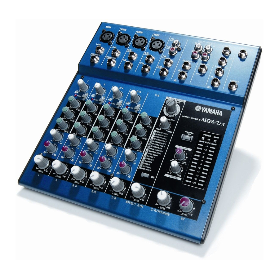
http://www.xiaoyu163.com MG8 / 2FX PANEL LAYOUT(パネルレイアウト) 3 7 63 1515 0 ■ ■ ■ ■ ■ Channel Control Section(チャンネルコントロール部) Channels Channels Channels 1 and 2 3/4 and 5/6 (Monaural) (Stereo) (Stereo) q [GAIN] Control w [PEAK] Indicator ] Switch (High Pass Filter) r Equalizer ([HIGH], [MID], [LOW]) t [EFFECT] Controls y [PAN] Controls (CHs 1 and 2) - Page 9 http://www.xiaoyu163.com MG8 / 2FX 3 7 63 1515 0 ■ ■ ■ ■ ■ Input/Output Section(入出力部) Channel Input Jacks (CHs 1, 2, 3/4, 5/6) チャンネル INPUT 端子 (CH 1, 2, 3/4, 5/6) [MIC] Jacks [MIC] 端子 [LINE] Jacks [LINE] 端子 [INSERT I/0] 端子...
- Page 10 http://www.xiaoyu163.com MG8 / 2FX 3 7 63 1515 0 Connector Polarities INPUT OUTPUT Pin 1: Ground MIC INPUT Pin 2: Hot (+) Pin 3: Cold (-) LINE INPUT (monaural channels), Tip: Hot (+) ST OUT, C-R OUT Ring: Cold (-) EFFECT * Sleeve: Ground Ring...
-
Page 11: Disassembly Procedure(分解手順
Support Stand [240] (MAINシート) (サポートスタンド) [240]: Bind Head Tapping Screw-S 3.0X6 MFZN2BL(EP630210) [160]: Spacer MG8/2FX (WD237400) スペーサー MIX +バインドSタイト [265]: Cap Screw 3X25 MFZNBL (WD251500) 6 角孔付き P タイト [260]: Bind Head Tapping Screw-B 3.0X8 MFZN2BL (EP600190) +バインド B タイト... - Page 12 http://www.xiaoyu163.com MG8 / 2FX 3 7 63 1515 0 [130] Cover (カバー) Top Cover DSP Circuit Board (トップカバー) (DSPシート) [110] [263] Connector CNM02 (コネクターCNM02) Shield (シールド) Power Switch and AC Connector MAIN Circuit Board (電源スイッチとACコネクター) (MAINシート) Connector CNE01 (コネクターCNE01) [263]: Bind Head Tapping Screw-S 3.0X6 MFZN2BL (EP630210) [110]: Bind Head Tapping Screw-S 3.0X6 MFZN2BL (EP630210) +バインド...
- Page 13 http://www.xiaoyu163.com MG8 / 2FX 3 7 63 1515 0 Hexagonal nut & Washer (六角ナット、ワッシャー) [180a] [180b] Top Cover (トップカバー) [300] Guard (ガード) [190] [200] [180]: Bonding Tapping Screw-B 3.0X10 MFZN2BL (VQ049800) ボンディング B タイト [190]: Knob WHITE/M-GLAY (WA009900) ノブ LEVEL [200]: Knob RED/M-GRAY (WA010000) ノブ...
- Page 14 http://www.xiaoyu163.com MG8 / 2FX 3 7 63 1515 0 Note: When reassembling the MAIN circuit board and the 注)MAIN シートとトップカバーの再組立時に、LED の頭とスペーサーがパネルの穴から正しく出て top cover, confirm whether the heads of LEDs and いるか注意して下さい。 ( Fig.9) spacers correctly come out of the corresponding holes on the top cover.(Fig.9) (LED) (Spacer)
-
Page 15: Lsi Pin Description( Lsi 端子機能表
http://www.xiaoyu163.com MG8 / 2FX LSI PIN DESCRIPTION (LSI 端子機能表) 3 7 63 1515 0 • YMW767-V (X3271A00) CPU DSP: ICM07 NAME FUNCTION NAME FUNCTION TESTN Input for TEST IOVDD IOVDD +3.3V PLLBPN PLL bypass select LBN/LWRN/PF6 External memory lower-byte enable PLLVDD PLLVDD +2.5V UBN/UWRN/PF7... -
Page 16: Ic Block Diagram(Ic ブロック図
http://www.xiaoyu163.com MG8 / 2FX IC BLOCK DIAGRAM (IC ブロック図) 3 7 63 1515 0 PCM1742KEG/2K (X3538A00) Digital to Analog Converter DSP: ICM08 PIN ASSIGNMENTS NAME TYPE FUNCTION Audio Data Bit Clock Input. DATA Audio Data Digital Input. DATA LRCK L-Channel and R-Channel Audio Data Latch En- Audio LRCK LRCK... - Page 17 http://www.xiaoyu163.com MG8 / 2FX CIRCUIT BOARDS (シート基板図) 3 7 63 1515 0 CONTENTS MAIN Circuit Board (X5023B0) ................... 18-21 DSP Circuit Board (X5022C0) ....................17 • DSP Circuit Board L 13942296513 To MAIN-CNE01 Component Side(部品側) Pattern Side(パターン側) u163 Note:See parts list for details of circuit board component parts. 注:シートの部品詳細はパーツリストをご参照ください。...
- Page 18 http://www.xiaoyu163.com MG8 / 2FX 3 7 63 1515 0 • MAIN Circuit Board IC01-IC05, Q01 PHONES Apply silicon grease to the shaded area FOOT before installing ICs 01-05 and Q01 on SWITCH the heat sink. 放熱板に取り付ける前に斜線部にシリコン グリスを塗ること。 ST OUT ST OUT C-R OUT C-R OUT SEND...
- Page 19 http://www.xiaoyu163.com MG8 / 2FX 3 7 63 1515 0 PEAK to DSP-CNM02 HONES POWER R OUT RETURN 2TR IN C-R / PHONES PHANTOM +48V PROGRAM PARAMETER EFFECT TURN L 13942296513 PAN/BAL PEAK PAN/BAL PEAK SERT PEAK SERT PEAK u163 GAIN PEAK HIGH EFFECT...
- Page 20 http://www.xiaoyu163.com MG8 / 2FX 3 7 63 1515 0 • MAIN Circuit Board L 13942296513 u163 http://www.xiaoyu163.com...
- Page 21 http://www.xiaoyu163.com MG8 / 2FX 3 7 63 1515 0 BROWN to AC ADAPTOR IN WD35000 Wiring Ass'y AC8 ON/STANDBY BLACK L 13942296513 u163 Pattern Side(パターン側) 2NA-WC28110 http://www.xiaoyu163.com...
- Page 22 http://www.xiaoyu163.com MG8 / 2FX INSPECTIONS 3 7 63 1515 0 Power Supply AC Adaptor shall be used. W0703500(U,V:120V), WC711000(O:220V), WC703800(K:220V), WC703700(B:230V), WC703600(H,W:230V), WC703900(A:240V), WC703400(J:100V) Power Indicator and Effect On LED Inspection POWER LED &DIGITAL EFFECT ON LED shall light when the unit is turned on. Next, turn off the DIGITAL EFFECT ON switch.(Then, LED shall be off.) Mixer Section Inspection 3.1 Preparation...
- Page 23 http://www.xiaoyu163.com MG8 / 2FX 3 7 63 1515 0 3.2 Gain The output levels shall be within the range specified in the Table 3.2-1 to 3.2-6. Table 3.2-1 [CH INPUT(1, 2)] [Unit: dBu] INPUT INPUT Level Gain ST L OUT ST R OUT SEND/EFFECT C-R OUT L C-R OUT R...
- Page 24 http://www.xiaoyu163.com MG8 / 2FX 3 7 63 1515 0 3.3 Frequency Characteristics In the signal routes of the Table 3.2-1 to 3.2-6 indicated with (1) to (12), the 20Hz and 20kHz frequency response of each output shall be within the range of 0 dB +1/-2.5 dB compared to the 1kHz(0dB). *The 20Hz level when the GAIN volume is Max shall be within the range of 0 dB +1.0/-4.5 dB compared to the 1kHz (0dB).
- Page 25 http://www.xiaoyu163.com MG8 / 2FX 3 7 63 1515 0 At the C-R OUT (L/R), setting the Level Control to the 12 o’clock position, feeding each 20Hz, 1kHz and 20kHz signal, the distortion shall be less than 0.2%, when the output signal level is +3dBu. *In the route (1), check every OUT when the signal is fed to CH1,and check only the ST L OUT when the signal is fed to CH2 and other channels.
- Page 26 http://www.xiaoyu163.com MG8 / 2FX 3 7 63 1515 0 3.15 Others DIGITAL EFFECT(Confirmation by Hearing Test) Before testing, set the controls as shown below. EFFECT VR: Max.(10), PROGRAM: 1, EFFECT: ON, EFFECT RTN VR: Max.(10) Feed a sound source at an appropriate level to CH1 and confirm whether the reverb sound is heard at the PHONES. Foot Switch(Confirmation) Confirm that the EFFECT is turned on and off correctly when the foot switch is pressed and released.
- Page 27 http://www.xiaoyu163.com MG8 / 2FX 検査 3 7 63 1515 0 1 . 1 . 1 . 1 . 1 . 電 源 電 源 電 源 電 源 電 源 AC アダプターを使用します。 *AC アダプター(100V: WC703400) 2 . 2 . 2 . 2 . 2 . パワーインジケーターと...
- Page 28 http://www.xiaoyu163.com MG8 / 2FX 3 7 63 1515 0 3 . 2 3 . 2 3 . 2 利 得 利 得 利 得 3 . 2 3 . 2 利 得 利 得 3.1 項の状態で各出力端子には[Table 3.2-1 ∼ 3.2-6]の範囲内の出力レベルが得られることを確認します。 Table 3.2-1 [CH INPUT Table 3.2-1 [CH INPUT(...
- Page 29 http://www.xiaoyu163.com MG8 / 2FX 3 7 63 1515 0 3 . 3 3 . 3 周 波 数 特 性 3 . 3 周 波 数 特 性 周 波 数 特 性 周 波 数 特 性 3 . 3 3 .
- Page 30 http://www.xiaoyu163.com MG8 / 2FX 3 7 63 1515 0 3 . 9 3 . 9 3 . 9 歪 率 歪 率 歪 率 3 . 9 3 . 9 歪 率 歪 率 Table 3.2-1 ∼ 3.2-6 の(1)∼(12)の印のついた系統において( (3) 、 (4)を除く) 、20Hz, 1kHz, 20kHz の 入力に対して...
- Page 31 http://www.xiaoyu163.com MG8 / 2FX 3 7 63 1515 0 Table 3.14-1 [ Table 3.14-1 [ Table 3.14-1 [単 位 Table 3.14-1 [ Table 3.14-1 [ 単 位 単 位 単 位 単 位: d B u ] : d B u ] : d B u ] : d B u ] : d B u ]...
-
Page 32: Http://Www.xiaoyu163.Com
http://www.xiaoyu163.com 3 7 63 1515 0 PARTS LIST CONTENTS(目次) OVERALL ASSEMBLY (総組立) ..................2 ELECTRICAL PARTS (電気部品) .................. 4 Note) DESTINATION ABBREVIATIONS L 13942296513 Australian model Chinese model British model South-east Asia model Canadian model Taiwan model German model U.S.A. model European model General export model (110V) French model... - Page 33 http://www.xiaoyu163.com MG8 / 2FX ■ OVERALL ASSEMBLY (総組立) 3 7 63 1515 0 Hexagon nut & Washer(六角ナット,ワッシャー) Accessories of Phone Jack(ホーンジャックの付属品) L 13942296513 u163 http://www.xiaoyu163.com...
- Page 34 品 名 REMARKS PART NO. REF NO. QTY RANK Overall Assembly 総 組 立 MG8/2FX Overall Assembly MG8/2FX J Y 総 組 立 (WC62680) WC281100 Circuit Board MAIN MG8/2FX M A I N シ ー ト (X5023B0) ∗ Shield MG8/2FX シ...
- Page 35 部 品 名 REMARKS REF NO. QTY RANK ELECTRICAL PARTS 電 気 部 品 MG8/2FX WC281100 Circuit Board MAIN MG8/2FX M A I N シ ー ト (X5023B0) ∗ WC281000 Circuit Board D S P シ ー ト (WD80120)(X5022C0) ∗...
- Page 36 http://www.xiaoyu163.com MG8 / 2FX 3 7 63 1515 0 PART NO. DESCRIPTION 部 品 名 REMARKS REF NO. QTY RANK UR838100 C144 Electrolytic Cap. 100.00 16.0V ケ ミ コ ン UR838100 C145 Electrolytic Cap. 100.00 16.0V ケ ミ コ ン V J 0 9 7 4 0 0 C201 Electrolytic Cap.-KL...
- Page 37 http://www.xiaoyu163.com MG8 / 2FX 3 7 63 1515 0 PART NO. DESCRIPTION 部 品 名 REMARKS REF NO. QTY RANK UA653390 C335 Mylar Capacitor 3900P 50V J マ イ ラ ー コ ン UA653390 C336 Mylar Capacitor 3900P 50V J マ...
- Page 38 http://www.xiaoyu163.com MG8 / 2FX 3 7 63 1515 0 PART NO. DESCRIPTION 部 品 名 REMARKS REF NO. QTY RANK US061470 C451 Ceramic Capacitor-CH(chip) 47P 50V J チ ッ プ セ ラ ( C H ) UR847470 C452 Electrolytic Cap. 47.00 25.0V ケ...
- Page 39 http://www.xiaoyu163.com MG8 / 2FX 3 7 63 1515 0 PART NO. DESCRIPTION 部 品 名 REMARKS REF NO. QTY RANK US061470 C808 Ceramic Capacitor-CH(chip) 47P 50V J チ ッ プ セ ラ ( C H ) UR866470 C809 Electrolytic Cap. 4.70 50.0V ケ...
- Page 40 http://www.xiaoyu163.com MG8 / 2FX 3 7 63 1515 0 PART NO. DESCRIPTION 部 品 名 REMARKS REF NO. QTY RANK X4928A00 IC05 KIA7805API I C REGULATOR +5V X5025A00 IC101 NJM4580M-D(TE2) I C OP AMP I G 1 0 3 5 2 0 IC103 NJM4558M(T1) I...
- Page 41 http://www.xiaoyu163.com MG8 / 2FX 3 7 63 1515 0 PART NO. DESCRIPTION 部 品 名 REMARKS REF NO. QTY RANK V 7 4 2 1 7 0 0 Q103 Transistor (chip) 2SC3324 GR,BL TE85 ト ラ ン ジ ス タ WC529400 Q104 Transistor...
- Page 42 http://www.xiaoyu163.com MG8 / 2FX 3 7 63 1515 0 PART NO. DESCRIPTION 部 品 名 REMARKS REF NO. QTY RANK RD358100 R141 Carbon Resistor (chip) 100.0K 63M J チ ッ プ 抵 抗 RD356820 R143 Carbon Resistor (chip) 8.2K 63M J チ...
- Page 43 http://www.xiaoyu163.com MG8 / 2FX 3 7 63 1515 0 PART NO. DESCRIPTION 部 品 名 REMARKS REF NO. QTY RANK RD357180 R256 Carbon Resistor (chip) 18.0K 63M J チ ッ プ 抵 抗 RD357360 R257 Carbon Resistor (chip) 36.0K 63M J チ...
- Page 44 http://www.xiaoyu163.com MG8 / 2FX 3 7 63 1515 0 PART NO. DESCRIPTION 部 品 名 REMARKS REF NO. QTY RANK RD356390 R380 Carbon Resistor (chip) 3.9K 63M J チ ッ プ 抵 抗 HB026680 R401 Metal Film Resistor 6.8K 1/4 F 金...
- Page 45 http://www.xiaoyu163.com MG8 / 2FX 3 7 63 1515 0 PART NO. DESCRIPTION 部 品 名 REMARKS REF NO. QTY RANK RD358220 R501 Carbon Resistor (chip) 220.0K 63M J チ ッ プ 抵 抗 RD358220 R502 Carbon Resistor (chip) 220.0K 63M J チ...
- Page 46 http://www.xiaoyu163.com MG8 / 2FX 3 7 63 1515 0 PART NO. DESCRIPTION 部 品 名 REMARKS REF NO. QTY RANK RD355220 R816 Carbon Resistor (chip) 220.0 63M J チ ッ プ 抵 抗 RD358100 R817 Carbon Resistor (chip) 100.0K 63M J チ...
- Page 47 http://www.xiaoyu163.com MG8 / 2FX 3 7 63 1515 0 PART NO. DESCRIPTION 部 品 名 REMARKS REF NO. QTY RANK V 8 2 6 4 7 0 0 -104 Rotary Variable Resistor B 50.0K XV09213P ロ ー タ リ ー V R V 8 2 6 4 6 0 0 VR105 Rotary Variable Resistor...
- Page 48 http://www.xiaoyu163.com MG8 / 2FX 3 7 63 1515 0 PART NO. DESCRIPTION 部 品 名 REMARKS REF NO. QTY RANK UF037100 CM43 Electrolytic Cap. (chip) 10 16V チ ッ プ ケ ミ コ ン UF037100 CM45 Electrolytic Cap. (chip) 10 16V チ...
- Page 49 http://www.xiaoyu163.com MG8 / 2FX 3 7 63 1515 0 PART NO. DESCRIPTION 部 品 名 REMARKS REF NO. QTY RANK RD356100 RM37 Carbon Resistor (chip) 1.0K 63M J チ ッ プ 抵 抗 RD356560 RM38 Carbon Resistor (chip) 5.6K 63M J チ...
-
Page 50: Circuit Diagram
http://www.xiaoyu163.com 3 7 63 1515 0 CIRCUIT DIAGRAM CONTENTS(目次) BLOCK DIAGRAM & LEVEL DIAGRAM (ブロックダイアグラム、レベルダイアグラム) ..OVERALL CIRCUIT DIAGRAM (総回路図) ( MA IN 1/5 ) ........................3 ( MAIN 2/5 ) ........................4 ( MAIN 3/5 ) ........................5 L 13942296513 ( MAIN 4/5 ) , ( MAIN 5/5 ) .................... - Page 51 3 7 6 3 1 5 1 5 0 BLOCK DIAGRAM & LEVEL DIAGRAM MG8/2FX MAIN SW102 JK101,201 Q101~104,IC101a LD102 Q201~204,IC201a IC802a IC804a SW101,201 JK802 LD101,201 IC103 VR107 IC101b,201b JK102,202 LEVEL IC202 VR207 VR801 LINE ST OUT GAIN VR102...
- Page 52 3 7 6 3 1 5 1 5 0 OVERALL CIRCUIT DIAGRAM 1/6 (MAIN 1/5) MG8/2FX MAIN To MAIN 2/5:A3 PHANTOM 3/5:J8 4/5:B4 OP AMP To MAIN 2/5:A3 LEVEL 3/5:I8 GAIN 4/5:B4 OP AMP OP AMP EFFECT To MAIN 2/5:A4...
- Page 53 3 7 6 3 1 5 1 5 0 OVERALL CIRCUIT DIAGRAM 2/6 ( MAIN 2/5 ) MG8/2FX MAIN OP AMP To MAIN 1/5:A1 3/5:J8 OP AMP (-10dBu) 4/5:B4 HIGH OP AMP To MAIN 1/5:A1 OP AMP 3/5:I8 4/5:B4...
- Page 54 http://www.xiaoyu163.com 3 7 6 3 1 5 1 5 0 From MAIN 1/5:A1 2/5:A3 4/5:B4 OP AMP OP AMP ST OUT From MAIN 1/5:A1 2/5:A3 OP AMP 4/5:B4 OP AMP To MAIN 2/5:P8 To MAIN 2/5:Q8 To MAIN 4/5:F4 From MAIN 1/5:A2 SEND (+4dBu) 2/5:A4...
- Page 55 3 7 6 3 1 5 1 5 0 ■ OVERALL CIRCUIT DIAGRAM 4/6 (MAIN 4/5) MG8/2FX MAIN PROGRAM To DSP-CNM02 PARAMETER EFFECT RTN From MAIN 3/5:I6 To MAIN 1/5:A1, 2/5:A3, 3/5:J8 To MAIN 1/5:A1, 2/5:A3, 3/5:I8 FOOT SWITCH Note: See parts list for details of circuit board component parts.
- Page 56 MG8/2FX 3 7 6 3 1 5 1 5 0 OVERALL CIRCUIT DIAGRAM 6/6 (DSP) MASK ROM RESET For JTAG Serial I/F 1 3 9 4 2 2 9 6 5 1 3 Not connected Not install OP AMP...