Yamaha RX-V359 Service Manual
Hide thumbs
Also See for RX-V359:
- Owner's manual (338 pages) ,
- Owner's manual (74 pages) ,
- Owner's manual (74 pages)
Table of Contents
Advertisement
Quick Links
RX-V359/HTR-5930
This manual has been provided for the use of authorized YAMAHA Retailers and their service personnel.
It has been assumed that basic service procedures inherent to the industry, and more specifically YAMAHA Products, are already
known and understood by the users, and have therefore not been restated.
WARNING:
IMPORTANT:
The data provided is believed to be accurate and applicable to the unit(s) indicated on the cover. The research, engineering, and
service departments of YAMAHA are continually striving to improve YAMAHA products. Modifications are, therefore, inevitable
and specifications are subject to change without notice or obligation to retrofit. Should any discrepancy appear to exist, please
contact the distributor's Service Division.
WARNING:
IMPORTANT:
I CONTENTS
To Service Personnel ...................................... 2~3
Impedance Selector ............................................. 3
Front Panels ........................................................ 3~5
Rear Panels .......................................................... 5~9
Remote Control Panels .................................... 10
Specifications .................................................. 11~12
Internal View ......................................................... 12
Disassembly Procedures ........................... 13~15
Self Diagnosis Function (Diag) ................. 16~33
Confirmation Of Idling Current ................... 34
1 0 0 9 9 5
SERVICE MANUAL
IMPORTANT NOTICE
Failure to follow appropriate service and safety procedures when servicing this product may result in personal
injury, destruction of expensive components, and failure of the product to perform as specified. For these reasons,
we advise all YAMAHA product owners that any service required should be performed by an authorized
YAMAHA Retailer or the appointed service representative.
The presentation or sale of this manual to any individual or firm does not constitute authorization, certification or
recognition of any applicable technical capabilities, or establish a principle-agent relationship of any form.
Static discharges can destroy expensive components. Discharge any static electricity your body may have
accumulated by grounding yourself to the ground buss in the unit (heavy gauge black wires connect to this buss).
Turn the unit OFF during disassembly and part replacement. Recheck all work before you apply power to the unit.
Display Data ..................................................... 35~36
Ic Data ................................................................. 37~43
Printed Circuit Board .................................. 45~52
Pin Connection Diagram .............................. 53~54
Block Diagram ....................................................... 55
Schematic Diagrams ...................................... 56~60
Replacement Parts List .............................. 61~69
Remote Control .............................................. 70~71
Advanced Setup .............................................. 72~73
2006
All rights reserved.
This manual is copyrighted by YAMAHA and may not be copied or
redistributed either in print or electronically without permission.
AV RECEIVER
P.O.Box 1, Hamamatsu, Japan
'06.01
Advertisement
Table of Contents

Related Manuals for Yamaha RX-V359


Summary of Contents for Yamaha RX-V359
-
Page 1: Service Manual
This manual has been provided for the use of authorized YAMAHA Retailers and their service personnel. It has been assumed that basic service procedures inherent to the industry, and more specifically YAMAHA Products, are already known and understood by the users, and have therefore not been restated. -
Page 2: To Service Personnel
RX-V359/HTR-5930 I TO SERVICE PERSONNEL 1. Critical Components Information AC LEAKAGE WALL EQUIPMENT TESTER OR Components having special characteristics are marked s and OUTLET UNDER TEST EQUIVALENT must be replaced with parts having specifications equal to those originally installed. 2. Leakage Current Measurement (For 120V Models Only) -
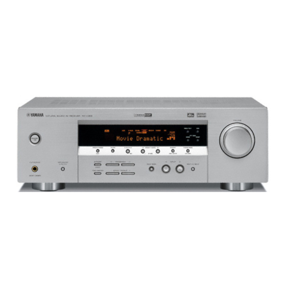
Page 3: Front Panels
I IMPEDANCE SELECTOR U, C models IMPEDANCE SELECTOR WARNING: Do not change the IMPEDANCE SELECTOR switch setting while the power to this unit is on, otherwise this unit may be damaged. I FRONT PANELS RX-V359 (C model) - Page 4 RX-V359/HTR-5930 RX-V359 (R, T, K, A, L models) RX-V359 (B, G, E models) HTR-5930 (U, C models)
-
Page 5: Rear Panels
RX-V359/HTR-5930 HTR-5930 (R, T, K, A models) HTR-5930 (B, G, E models) I REAR PANELS RX-V359 (C model) - Page 6 RX-V359/HTR-5930 RX-V359 (R model) RX-V359 (T model) RX-V359 (K model)
- Page 7 RX-V359/HTR-5930 RX-V359 (A model) RX-V359 (B, G, E models) RX-V359 (L model)
- Page 8 RX-V359/HTR-5930 HTR-5930 (U, C models) HTR-5930 (R model) HTR-5930 (T model)
- Page 9 RX-V359/HTR-5930 HTR-5930 (K model) HTR-5930 (A model) HTR-5930 (B, G, E models)
-
Page 10: Remote Control Panels
RX-V359/HTR-5930 I REMOTE CONTROL PANELS RX-V359 (C, R, T, K, A, L models) RX-V359 (B, G, E models) HTR-5930 (U, C, R, T, K, A models) HTR-5930 (B, G, E models) -
Page 11: Specifications
R, T, K, A, B, G, E, L models ......100 W 5ch Drive, 10 % THD .......... 510 W SUBWOOFER (L.P.F.) ....90 Hz / 18 dB oct. “SILENT CINEMA” is a trademark of YAMAHA CORPORATION. SURROUND L/R Dimensions (W x H x D) U, C models ........ -
Page 12: Internal View
RX-V359/HTR-5930 • Set Menu Table I INTERNAL VIEW The value inside of [ ] shows initial setting. Category No. MAIN MENU SUB MENU VALUE [INITIAL] MAIN (2) P.C.B. SETUP ROOM: S >M L S/[M]/L MAIN (4) P.C.B. (U, C models) -
Page 13: Disassembly Procedures
RX-V359/HTR-5930 I DISASSEMBLY PROCEDURES (Remove parts in the order as numbered.) Disconnect the power cable from the AC outlet. 2. Removal of Front Panel Unit 1. Removal of Top Cover a. Remove 4 screws (1), 4 screws (2) and 1 screw (3). - Page 14 RX-V359/HTR-5930 3. Removal of MAIN (3), MAIN (5), FUNCTION (3), FUNCTION (6) P.C.B.s and Tuner a. Remove CB242. (Fig. 2) e. Remove 4 screws (7). (Fig. 3) b. Remove 12 screws (5). (Fig. 3) f. Remove 2 (U, C, R, L models) screws (8). (Fig. 3) c.
- Page 15 RX-V359/HTR-5930 4. Removal of MAIN (1), DSP, FUNCTION (1), FUNCTION (8) and FUNCTION (9) P.C.B.s a. Remove 1 screw (9). (Fig. 4) f. Remove 4 screws (A). (Fig. 4) b. Remove CB803. (Fig. 4) g. Remove MAIN (1), DSP, FUNCTION (4), FUNCTION c.
- Page 16 RX-V359/HTR-5930 I SELF DIAGNOSIS FUNCTION (DIAG) There are 16 DIAG menu items, each of which has sub-menu items. Listed in the table below are menu items and sub-menu items. Note that not all menu items listed will apply to the models covered in this service manual.
- Page 17 RX-V359/HTR-5930 No DIAG menu sub-menu 4. XM Tone /44.1k 5. ISO Tone /44.1k 6. 1k -1dB /32k 7. 1k -61dB /32k 8. Mute /32k 9. XM Tone /32k 10. ISO Tone /32k 11. XM/DT Bus Power: OFF 12 IF STATUS 1.
- Page 18 RX-V359/HTR-5930 • Starting DIAG • Display provided when DIAG started Press the “STANDBY/ON” key while simultaneously The FL display of the main unit displays the protection pressing those two keys of the main unit as indicated in the function history data and the version (1 alphabet) and the figure below.
- Page 19 RX-V359/HTR-5930 • Operation procedure of DIAG menu and When there is a history of protection Version (1 alphabet) function due to abnormal DC output SUB-MENU There are 15 MENU items, each of which has some SUB- MENU items. Cause: DC output of the power amplifier is abnormal.
- Page 20 RX-V359/HTR-5930 • Details of DIAG menu With full-bit output specified in some modes, it is possible to execute 0dBFS output without including the head margin in each channel. 1. DSP THROUGH Main DSP of YSS938 is selected for Front L/R output.
- Page 21 RX-V359/HTR-5930 DSP BYPASS YSS948 Main DSP Sub DSP Digital FL/FR SL/SR SWFR FL/FR Analog (Shaded items not used in this example) YSS FULL BIT P • The Presence CH signal is output in digital full bit at the Front CH.
- Page 22 RX-V359/HTR-5930 2. RAM THROUGH This function is for YSS948 only. Only the CT signal is output through the Sub DSP – DRAM. RAM FULL BIT SPEAKER OUTPUT ( 1kHz ) SUBWOOFER Input level Volume FRONT OUTPUT CENTER SL/SR (50Hz) Both ch, -20 dBm +6.0 dB +11.5 dB +11.5 dB +11.5 dB...
- Page 23 RX-V359/HTR-5930 3. PRO LOGIC PRO LOGIC I PRO LOGIC II Reference data Reference data INPUT: DVD ANALOG INPUT: DVD ANALOG SWFR: 50Hz, Others: 1kHz SWFR: 50Hz, Others: 1kHz SPEAKER OUTPUT ( 1kHz ) SUBWOOFER SPEAKER OUTPUT ( 1kHz ) SUBWOOFER...
- Page 24 RX-V359/HTR-5930 4. SPEAKERS SET The input signal is automatically identified and switched in The signals output from the DSP block are the same as 1. the priority order of dts → DOLBY DIGITAL → PCM DSP THROUGH: YSS 0dB. AUDIO → Analog (A/D) according to the signal detection.
- Page 25 RX-V359/HTR-5930 5. HP Test The signal is output including the head margin. FRONT 15dB MARGIN FRONT 12dB MARGIN Reference data Reference data INPUT: DVD ANALOG INPUT: DVD ANALOG SWFR: 50Hz, Others: 1kHz SWFR: 50Hz, Others: 1kHz SPEAKER OUTPUT ( 1kHz ) SUBWOOFER...
- Page 26 RX-V359/HTR-5930 7. DISPLAY CHECK Segment conditions of the FL driver and the FL tube are This program is used to check the FL display section. The checked by turning ON and OFF all segments. Next, the display condition varies as shown below according to the operation of the FL driver is checked by using the dimmer sub-menu operation.
- Page 27 RX-V359/HTR-5930 9. FACTORY PRESET This menu is used to reserve and inhibit initialization of the back-up RAM. The signals are processed using EFFECT OFF. (The L/R signal is output using ANALOG FRONT BYPASS.) PRESET INHIBIT (Initialization inhibited) RAM initialization is not executed. Select this sub-menu to protect the values set by the user.
- Page 28 RX-V359/HTR-5930 10. AD DATA CHECK/FAN TEST K0/K1 (Panel key of main unit) (Reference: 5V=100%) This menu is used to display the A/D conversion value of A/D of the key fails to function properly when the standard the terminals which detects panel keys of the main unit value is deviated.
- Page 29 RX-V359/HTR-5930 11. XM STATUS (U, C models) The output check of XM Radio Antenna is executed. 1k -1dB/44.1k XM Tone/32k The test tone (1kHz, -1dB/44.1kHz) is output. The XM tone (32kHz) is output. 1k -61dB/44.1k ISO Tone/32k The test tone (1kHz, -61dB/44.1kHz) is output.
- Page 30 RX-V359/HTR-5930 12. IF STATUS (Input function status) (Not applied to these models.) Using the sub-menu, the status data is displayed one after 5th byte another in the hexadecimal notation. 4th byte During signal processing, the status before execution of 3rd byte this menu is maintained.
- Page 31 RX-V359/HTR-5930 CS1-5: Indicates channel status information of the input MTT: Mute trigger signal (IEC60958). Byte No. Function Mute condition Factor of the last mute BY1-4: Indicates information of the bit stream included in Error count of YSS938-FSCNT the DOLBY DIGITAL signal.
- Page 32 RX-V359/HTR-5930 14. SD DL CODE 15. SOFT SW (Not applied to these models.) This menu is used to switch the function settings on the This menu is used to display the data version of the P.C.B. through the software so as to activate the product.
- Page 33 RX-V359/HTR-5930 16. MICROPROCESSOR INFORMATION The version, checksum and the port specified by the microprocessor are displayed. The signal is processed using EFFECT OFF. The checksum is obtained by adding the data at every 8 bits for each program area and expressing the result as a 4-figure hexadecimal data.
- Page 34 RX-V359/HTR-5930 I CONFIRMATION OF IDLING CURRENT Confirmation of Idling Current of MAIN (1) P. C. B. • Right after the power is turned on, confirm that the voltage across the terminals of R157 (FRONT Lch), R158 (FRONT Rch), R148 (CENTER), R156 (SURROUND Lch), R159 (SURROUND Rch) are between 0.1mV and 10.0mV.
-
Page 35: Display Data
RX-V359/HTR-5930 I DISPLAY DATA G V551 : 17-BT-24GNK (WE289300) PATTERN AREA G PIN CONNECTION Pin No. Connection Pin No. Connection Note : 1) F1, F2 ..Filament 2) NP ..No pin 3) NX ..No extened pin 4) DL ..Datum line 5) 1G ~ 16G .. - Page 36 RX-V359/HTR-5930 G ANODE CONNECTION 13G~2G – – – – – – – – – – – – – – – – – – – – – – – – – –...
- Page 37 RX-V359/HTR-5930 I IC DATA IC242: M30622MWP-A82FP (MAIN P.C.B.) 16-bit Microprocessor PURD /BLK DTZ2 DKZ2 ONEA /MTFS ONEB /MTZ2 /MTSW /MTCT /EMP /MTHP PLDET ADKEY0 SCKN ADKEY1 SDRN/DEST AVss SDTN MODEL VREF CLKF AVcc RXDF CEFD TXDF Port Name Terminal Name...
- Page 38 RX-V359/HTR-5930 IC242: M30622MWP-A82FP (MAIN P.C.B.) 16-bit Microprocessor Port Name Terminal Name Function PowerOn Standby Sleep P65/CLK1 CLKF Serial clock of Flash ROM clock P64/CTS1/RTS1/CTS0/CLKS1 BUSY signal output of Flash ROM clock P63/TXD0/SDA0 DTXM Serial data transmission for XM IC (UART0)
- Page 39 RX-V359/HTR-5930 IC242: M30622MWP-A82FP (MAIN P.C.B.) 16-bit Microprocessor Port Name Terminal Name Function PowerOn Standby Sleep P107/AN7/KI3 – No used P106/AN6/KI2 AD protection DC detection P105/AN5/KI1 PLDET AD power limitter detection P104/AN4/KI0 AD temperature detection P103/AN3 IMP_6 ohms Speaker impedance detection (H: 6 ohms/L: 8 ohms)
- Page 40 RX-V359/HTR-5930 IC811: YSS948-VZ (DSP P.C.B.) VDD2 AHVSS VDD2 AHVSSG DVSS DVDD MEMD7 VDD2 MEMD6 VDD2 MEMD5 MEMD4 VDD1 VDD1 MEMD3 STATUS4 MEMD2 STATUS5 MEMD1 STATUS6 MEMD0 STATUS7 VDD2 VDD2 TEST MEMA0 TEST MEMA1 YSS948-VZ MEMA2 VDD2 VDD2 VDD2 VDD2 VDD1...
- Page 41 RX-V359/HTR-5930 IC811: YSS948-VZ (DSP P.C.B.) Pin Name Classification Function Port Set Size Connect AHVSS PLL section GND DGND AHVSSG PLL section GND DGND DVSS PLL section GND DGND DVDD Power supply Internal power supply of PLL section (typ1.2V) +1.2VPLL VDD2 Internal power supply (typ1.2V)
- Page 42 RX-V359/HTR-5930 IC811: YSS948-VZ (DSP P.C.B.) Pin Name Classification Function Port Set Size Connect DGND DGND VDD2 Power supply Internal power supply (typ1.2V) +1.2V VDD2 Internal power supply (typ1.2V) +1.2V MEMA8 External memory IF External memory access output terminal 8 EXMA8...
- Page 43 RX-V359/HTR-5930 IC811: YSS948-VZ (DSP P.C.B.) Pin Name Classification Function Port Set Size Connect VDD1 External power supply (typ3.3V) +3.3V MISO Microprocessor IF Data output SDD3 DGND MISI Microprocessor IF Data input SDM3A MISCK Serial clock SCK3A nMICS Chip select /CSADM...
- Page 44 RX-V359/HTR-5930 MEMO...
- Page 45 RX-V359/HTR-5930 I PRINTED CIRCUIT BOARD DIGITAL INPUT DSP P.C.B. DSP P.C.B. (Side A) (Side B) COAXIAL OPTICAL Lead Free Solder Used Lead Free Solder Used DTV/CBL U, C models U, C models MAIN (1) (CB247) +5BUS FSCXM DGND /ICXM DTXM DRXM •...
- Page 46 RX-V359/HTR-5930 I PRINTED CIRCUIT BOARD • Semiconductor Location Ref no. Location FUNCTION (1) P.C.B. FUNCTION (1) P.C.B. (Side A) (Side B) D451 D452 Lead Free Solder Used IC451 MULTI CH INPUT AUDIO IC452 IC453 FRONT SURROUND SUBWOOFER MD/CD-R IC454 / CENTER...
- Page 47 RX-V359/HTR-5930 I PRINTED CIRCUIT BOARD FUNCTION (2) P.C.B. (Side A) FUNCTION (4) • Semiconductor Location (CB653) Ref no. Location D551 D552 IC551 B, G, E models Q551 FREQ/TEXT Q552 FUNCTION (5) Q553 VOLUME (CB671) Q554 PTY SEEK Q555 FL DISPLAY...
- Page 48 RX-V359/HTR-5930 I PRINTED CIRCUIT BOARD FUNCTION (3) P.C.B. FUNCTION (4) P.C.B. (Side A) (Side A) MAIN (1) AUDIO OUTPUT (CB246) DTV/CBL V-AUX SUBWOOFER from TRANSFORMER FUNCTION (2) (CB552) FUNCTION (6) (CB676) FUNCTION (3) P.C.B. (Side B) Lead Free Solder Used FUNCTION (4) P.C.B.
- Page 49 RX-V359/HTR-5930 I PRINTED CIRCUIT BOARD FUNCTION (7) P.C.B. (Side A) R, L models FUNCTION (5) P.C.B. FUNCTION (5) P.C.B. FUNCTION (6) P.C.B. (Side A) (Side B) (Side A) from TRANSFORMER Lead Free Solder Used SWMT SWMT FUNCTION (2) (CB553) • Semiconductor Location Ref no.
- Page 50 RX-V359/HTR-5930 I PRINTED CIRCUIT BOARD SPEAKERS FRONT COMP +10B + / - + / - TUNED MAIN (1) P.C.B. to TUNER PACK (Side A) SURROUND CENTER SDRP SCKP SDTP FRONT to ROM WRITER + / - + / - + / -...
- Page 51 RX-V359/HTR-5930 I PRINTED CIRCUIT BOARD MAIN (1) P.C.B. (Side B) Lead Free Solder Used 50 51 • Semiconductor Location Ref no. Location Ref no. Location D101 IC242 D102 Q101 D107 Q102 D110 Q103 D116 Q104 D241 Q105 D242 Q118 D243...
- Page 52 RX-V359/HTR-5930 I PRINTED CIRCUIT BOARD MAIN (4) P.C.B. (Side A) U, C models MAIN (3) P.C.B. MAIN (5) P.C.B. (Side A) (Side A) from TRANSFORMER MAIN (2) P.C.B. (Side A) VIDEO COMPONENT VIDEO DTV/CBL V-AUX MONITOR MONITOR OUT DTV/CBL Y / P...
-
Page 53: Pin Connection Diagram
RX-V359/HTR-5930 I PIN CONNECTION DIAGRAM • ICs KIA7805API KIA7912PI NJM2388F05 NJM2885DL1-33 PQ012FZ01ZP SN74AHCT1G32DCKR KIA7812API 2:GND 1:IN 3:OUT NJM4565M LA7956 SN74AHC08PWR MM74HCU04SJX LC72722PM SN74AHCT08PWR NJM2586AM SN74LV157APWR BS62LV256SC-70 STK433-130-E STK404-130Y AK4628AVQ M30622MWP-A82FP F2602E-01 LC89057W-VF4A-E M66003-0131FP BD3816K1-C YSS948-VZ... - Page 54 RX-V359/HTR-5930 • Diodes 1SS133,176 MTZJ12C 1SS355 1SS270A MTZJ30A KDS160-RTK Anode MTZJ4.7A MA8075-H Anode MA8100-H UDZ3.6B UDZ5.1B Cathode UDZ6.8B Cathode UDZS16B UDZS5.6B RB500V-40 UDZS6.2B 1SS380 UDZS9.1B 1SR154-400 KPB103G TS6P03G SB01-05Q TS4B03G Cathode Anode – – Anode Cathode • Transistors 2N5401C-AT 2SC1740S...
- Page 55 RX-V359/HTR-5930 BLOCK DIAGRAM VIDEO MAIN (5) FUNCTION (5) MAIN (1) MAIN (2) COMPONENT IC701 • See page 60 → SCHEMATIC DIAGRAM • See page 58 → SCHEMATIC DIAGRAM • See page 59 → SCHEMATIC DIAGRAM • See page 59 → SCHEMATIC DIAGRAM...
- Page 56 RX-V359/HTR-5930 SCHEMATIC DIAGRAM (DSP) Page 60 C10 Page 60 Page 57 to MAIN (1)_CB249 to MAIN (1)_CB247 to FUNCTION (1)_CB453 POINT A-1 Pin 29 of IC801 Page 58 to FUNCTION (2)_CB551 SRAM IC806: SN74AHCT08PWR IC951: SN74AHC08PWR QUADRUPLE 2-INPUT POSITIVE-AND GATES...
- Page 57 RX-V359/HTR-5930 SCHEMATIC DIAGRAM (FUNCTION 1/2) Page 60 Page 56 to MAIN (1)_CB244 to DSP_CB803 11.9 FRONT L -12.3 11.9 11.9 FUNCTION (6) CENTER -12.3 11.9 SURROUND L -7.7 -7.7 -7.0 -12.3 -12.3 FRONT L ANALOG IN 7CH VOLUME MUTE -12.3 11.9...
- Page 58 RX-V359/HTR-5930 SCHEMATIC DIAGRAM (FUNCTION 2/2) FL DISPLAY STANDBY/ON -22.3 -22.3 -22.3 -22.3 -20.4 -22.3 -16.8 -22.3 -18.5 -22.3 DRIVER TR -24.1 -22.3 -24.1 -22.2 FUNCTION (5) -22.4 -24.2 -18.7 -22.4 -20.4 -22.3 -22.5 -14.9 -16.6 -15.1 -24.1 -16.6 -25.9 -16.6 FL DRIVER -28.1...
- Page 59 RX-V359/HTR-5930 SCHEMATIC DIAGRAM (MAIN 1/2) IC101: STK404-130Y AF Power Amp L CH POWER AMP 49.3 49.2 MUTE SURROUND L -12.4 49.0 IC102, 103: STK433-130-E -12.4 Power Amp. SURROUND L FRONT L Driver Driver 49.0 Bias Circuit 48.8 48.2 48.9 5 4 6 7 Page 58 48.8...
- Page 60 RX-V359/HTR-5930 SCHEMATIC DIAGRAM (MAIN 2/2) POINT A-2 Pin 13 of IC242 POINT A-3 Pin 12 of IC241 IC241: LC72722PM IC391: LA7956 IC701: NJM2586AM RDS Signal Processor Video Switch Wide band 3-input 1-output 3-circuit video amplifier CH1 IN1 CH1 OUT Driver...
-
Page 61: Replacement Parts List
RX-V359/HTR-5930 I REPLACEMENT PARTS LIST • ELECTRICAL REPLACEMENT PARTS LIST WARNING Components having special characteristics are marked s and must be replaced with parts having specifications equal to those originally installed. ABBREVIATIONS IN THIS LIST ARE AS FOLLOWS: C.A.EL.CHP : CHIP ALUMI.ELECTROLYTIC CAP L.EMIT... - Page 62 RX-V359/HTR-5930 P.C.B. DSP P.C.B. DSP Ref. No. Part No. Description Markets Ref. No. Part No. Description Markets WG674000 P.C.B. C891 UR818100 C.EL 100uF 6.3V WG674100 P.C.B. RTKABGEL C894 US135100 C.CE.CHP 0.1uF C895-898 US061470 C.CE.CHP 47pF 50V B CB801-802 VQ961900 CN CB803 VQ044500 CN.BS.PIN...
- Page 63 RX-V359/HTR-5930 P.C.B. DSP & P.C.B. FUNCTION P.C.B. FUNCTION Ref. No. Part No. Description Markets Ref. No. Part No. Description Markets R961 R.CHP 22Ω 1/16W J C521-522 UR838100 C.EL 100uF R962 R.CHP 470KΩ 1/16W J C525-526 UR837100 C.EL 10uF R963 R.CHP 100KΩ...
- Page 64 RX-V359/HTR-5930 P.C.B. FUNCTION P.C.B. FUNCTION & P.C.B. MAIN Ref. No. Part No. Description Markets Ref. No. Part No. Description Markets IC456 X7378A00 IC NJM4565M(TE1) V551 WE289300 FL.DSPLY 17-BT-24GNK IC551 X6386A00 IC M66003-0131FP WA790800 SHEET WA790900 SPACER 4.6/10/32 s IC651 X4153A00 IC...
- Page 65 RX-V359/HTR-5930 P.C.B. MAIN P.C.B. MAIN Ref. No. Part No. Description Markets Ref. No. Part No. Description Markets C147 UR866470 C.EL 4.7uF C254 UR877470 C.EL 47uF C149 UR858100 C.EL 100uF C255 US064100 C.CE.CHP 0.01uF 50V B C150 UA654220 C.MYLAR 0.022uF 50V J C256 UR837470 C.EL...
- Page 66 RX-V359/HTR-5930 P.C.B. MAIN P.C.B. MAIN Ref. No. Part No. Description Markets Ref. No. Part No. Description Markets s D122 WA653200 DIODE.BRG TS6P03G 6.0A 200V Q250 WC435100 TR.DGT KRC104S-RTK D123 VD631600 DIODE 1SS133,176 Q251 iC174020 TR 2SC1740S QRS Q252 WC435100 TR.DGT...
- Page 67 RX-V359/HTR-5930 Replacement Parts List for Carbon Resistors P.C.B. MAIN Chip Resistors The chip resistor is not supplied as a replacement part. Ref. No. Part No. Description Markets Value 1/4W Type Part No. 1/6W Type Part No. Value 1/4W Type Part No. 1/6W Type Part No.
- Page 68 RX-V359/HTR-5930 • EXPLODED VIEW U, C models R, L models 1-1 (7) 1-25 1-1 (10) 1-25 1-25 1-1 (5) 1-1 (2) 2-104 2-104 U, C models B, G, E models 2-20 1-25 1-1 (8) 2-104 1-1 (4) 2-103 1-13 1-1 (3)
- Page 69 RX-V359/HTR-5930 • REPLACEMENT PARTS LIST Ref. No. Part No. Description Remarks Markets Ref. No. Part No. Description Remarks Markets WG673600 P.C.B. ASS'Y FUNCTION s 16 WC743700 POWER CABLE WG673700 P.C.B. ASS'Y FUNCTION s 16 WB212200 POWER CABLE WG673800 P.C.B. ASS'Y...
- Page 70 RX-V359/HTR-5930 I REMOTE CONTROL RAV309 (U, C, R, T, K, A, L models) • SCHEMATIC DIAGRAM • KEY CODE TABLE CODE Function CD-R TUNER DVD (P) DVD (Y) DVD (M) DVD-R (P) 0Ω TV POWER – – – – –...
- Page 71 RX-V359/HTR-5930 I REMOTE CONTROL RAV22 (B, G, E models) The schematic diagram is not available. • PANEL • KEY LAYOUT • CUSTOM CODE: 7A Data Code Name D-TV/CBL POWER MD/CD-R V-AUX 6CH INPUT TUNER A/B/C/D/E PRESET – PRESET + / DTS 6.1 / 5.1...
- Page 72 RX-V359/HTR-5930...
- Page 73 RX-V359/HTR-5930...
- Page 74 RX-V359/HTR-5930...