Sign In
Upload
Manuals
Brands
Tews Technologies Manuals
Control Unit
TAMC532
Tews Technologies TAMC532 Manuals
Manuals and User Guides for Tews Technologies TAMC532. We have
1
Tews Technologies TAMC532 manual available for free PDF download: User Manual
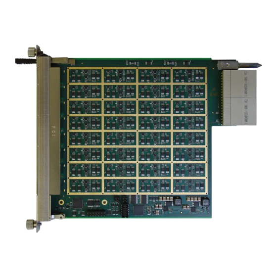
Tews Technologies TAMC532 User Manual (95 pages)
32 x 12/14 Bit 50/75 Msps ADC for MTCA.4 Rear-I/O
Brand:
Tews Technologies
| Category:
Control Unit
| Size: 1 MB
Table of Contents
Table of Contents
5
Product Description
11
Figure 1-1 : Block Diagram
11
Technical Specification
12
Table 2-1 : Technical Specification
12
Handling and Operating Instructions
13
ESD Protection
13
Thermal Considerations
13
I/O Signaling Voltages
13
Ipmi Support
14
Temperature and Voltage Sensors
14
FRU Information
14
Table 4-1 : Temperature and Voltage Sensors
14
Table 4-2 : Fru Information
14
Board Info Area
15
Product Info Area
15
Multi Record Area
15
Module Current Requirements
15
Table 4-3 : Board Info Area
15
Table 4-4 : Product Info Area
15
Table 4-5 : Module Current Requirements
15
AMC Point-To-Point Connectivity
16
Table 4-6 : Amc Point-To-Point Connectivity
16
Clock Configuration
17
Modifying FRU Records
17
Table 4-7 : Clock Configuration
17
Functional Description
18
Overview
18
Fpga
18
Interrupt Handling
18
Figure 5-1 : Functional Block Diagram
18
DMA Controller
19
ADC Data Acquisition
20
Table 5-1 : Maximum Sample Count Per Channel
21
Table 5-2 : Adc Data Alignment
22
I2C Bridge
23
Board Configuration Controller (BCC)
24
DDR3 Memory
25
Fabric Interfaces
25
PCI-Express
25
Figure 5-2 : Ddr3 Memory Interfaces
25
Figure 5-3 : Fabric Interfaces
25
Flash Memory
26
ADC Clocking
26
Figure 5-4 : Adc Clocking Overview
26
Crosspoint Switch
27
Lmk04806
27
Figure 5-5 : Adc Clock Generation and Distribution Structure
27
Vcxo
28
Adcs
28
Tclkb
28
Amc_Tclk
28
Amc_Clk0
28
Trigger and GPIO
29
Analog Inputs
29
Figure 5-6 : M-Lvds I/O
29
Figure 5-7 : Single Analog Input
29
ADC Sample Clock
30
Input Voltage Range
30
Figure 5-8 : 8 X Analog Input Group
30
Debug
31
Leds
31
Uart
31
Jtag
31
Reset
31
Μrtm Detection
31
Addressable Resources
32
Fpga
32
Structural Description
32
Figure 6-1 : Tamc532 Firmware Soc Structure
32
Pcie Configuration
33
Table 6-1 : Pcie Configuration Registers
33
Table 6-2 : Pcie Bar Overview
33
Register Interface
34
Module Control Register (0X00)
36
Table 6-3 : Module Register Space
36
Table 6-4 : Module Control Register (0X00)
36
Module Status Register (0X04)
37
Table 6-5 : Module Status Register (0X04)
38
Module Interrupt Enable Register (0X08)
39
Table 6-6 : Module Interrupt Enable Register (0X08)
41
Module Interrupt Status Register (0X0C)
42
ADC Channel [XX] Data Register
44
Table 6-7 : Module Interrupt Status Register (0X0C)
44
Table 6-8 : Adc Channel [XX] Data Register
44
I2C Bridge Control Register (0X50)
45
I2C Bridge Clock Divider Register (0X54)
46
I2C Bridge Status Register (0X58)
46
Table 6-9 : I2C Bridge Control Register (0X50)
46
Table 6-10 : I2C Bridge Clock Divider Register (0X54)
46
I2C Bridge Command Register (0X5C)
48
Table 6-11 : I2C Bridge Status Register (0X58)
48
I2C Bridge Write Data FIFO Interface Register (0X60)
49
I2C Bridge Read FIFO Data Register (0X64)
49
Table 6-12 : I2C Bridge Command Register (0X5C)
49
Table 6-13 : I2C Bridge Write Data Fifo Interface Register (0X60)
49
Table 6-14 : I2C Bridge Read Fifo Data Register (0X64)
49
DMA Controller [X] Control Register
50
DMA Controller [X] Status Register
50
Table 6-15 : Dma Controller [X] Control Register
50
DMA Controller [X] Base Descriptor Address Register
51
Table 6-16 : Dma Controller [X] Status Register
51
Table 6-17 : Dma Controller [X] Base Descriptor Address Register
51
DMA Controller [X] Current Memory Write Address Register
52
Table 6-18 : Dma Controller [X] Current Descriptor Address Register
52
Application Control Register (0X100)
53
Table 6-19 : Application Control Register (0X100)
53
CSPT Unit [X] Control Register
54
Table 6-20 : Cspt Unit [X] Control Register
55
CSPT Unit [X] Data Register #0 - Pre-Trigger Sample Count
56
CSPT Unit [X] Data Register #1 - Post-Trigger Sample Count
56
Application Status Register (0X160)
56
Table 6-21 : Cspt Unit [X] Data Register #0 - Pre-Trigger Sample Count
56
Table 6-22 : Cspt Unit [X] Data Register #1 - Post-Trigger Sample Count
56
Table 6-23 : Application Status Register (0X160)
57
Application Command Register (0X164)
58
Table 6-24 : Application Command Register (0X164)
58
Firmware Identification Register (0X1Fc)
59
Table 6-25 : Firmware Identification Register (0X1Fc)
59
DMA Descriptor Control DW
60
DMA Descriptor Next Descriptor Address
61
DMA Descriptor Data Memory Address
61
Reserved
61
Table 6-26 : Dma Descriptor Control Dw
61
Table 6-27 : Dma Descriptor Next Descriptor Address
61
Table 6-28 : Dma Descriptor Data Memory Address
61
Table 6-29 : Reserved
61
Board Configuration Controller (BCC)
62
Bcc-I2C
62
Table 6-30 : Bcc Target Register Space
62
LMK04816 Status Register (0X00)
63
Table 6-31 : Lmk04816 Status Register (0X00)
63
SI5338 Status Register (0X01)
64
Table 6-32 : Si5338 Status Register (0X01)
64
AMC Rx/Tx Differential Pair [X] Control Register
65
Table 6-33 : Amc Rx/Tx Differential Pair [X] Control Register
65
SFP Control Register (0X06)
66
Table 6-34 : Sfp Control Register (0X06)
66
SPI Control Register (0X07)
67
Table 6-35 : Spi Control Register (0X07)
67
Miscellaneous Register (0X09)
68
Table 6-37 : Miscellaneous Register (0X09)
68
Configuration DIP Switches Register (0X0A)
69
ADC Input Amplifiers Control Register (0X0B)
69
Table 6-38 : Configuration Dip Switches Register (0X0A)
69
Table 6-39 : Adc Input Amplifiers Control Register (0X0B)
71
Frequency Adjustment Control Register (0X0C)
72
BCC Firmware Identification Register (0Xfc)
72
Table 6-40 : Frequency Adjustment Control Register (0X0C)
72
Table 6-41 : Bcc Firmware Identification Register (0Xfc)
72
Configuration-I2C
73
BCC Bridge Register Space
73
Table 6-42 : Bcc Bridge Register Space
73
ADC Setup Interface Control Register (0X00)
74
Table 6-43 : Adc Setup Interface Control Register (0X00)
74
ADC Setup Interface Status Register (0X01)
75
ADC Setup Interface Lower Target Address Register (0X02)
75
ADC Setup Interface Upper Target Address Register (0X03)
75
Table 6-44 : Adc Setup Interface Status Register (0X01)
75
Table 6-45 : Adc Setup Interface Lower Target Address Register (0X02)
75
Table 6-46 : Adc Setup Interface Upper Target Address Register (0X03)
75
ADC Setup Interface Read Data (0X04)
76
ADC Setup Interface Write Data (0X05)
76
LMK Setup Interface Control Register (0X10)
76
Table 6-47 : Adc Setup Interface Read Data (0X04)
76
Table 6-48 : Adc Setup Interface Write Data (0X05)
76
Table 6-49 : Lmk Setup Interface Control Register (0X10)
76
LMK Setup Interface Status Register (0X11)
77
LMK Read Data Register [X]
77
Table 6-50 : Lmk Setup Interface Status Register (0X11)
77
Table 6-51 : Lmk Read Register [X]
77
LMK Write Data Register [X]
78
Table 6-52 : Lmk Write Register [X]
78
CPS Setup Interface Control Register (0X20)
79
CPS Setup Interface Status Register (0X21)
79
Table 6-53 : Cps Setup Interface Control Register (0X20)
79
Table 6-54 : Cps Setup Interface Read Data (0X21)
79
CPS Setup Interface Read Data (0X22)
80
Table 6-55 : Cps Setup Interface Read Data (0X22)
80
CPS Setup Interface Write Data (0X23)
81
Table 6-56 : Cps Setup Interface Write Data (0X23)
81
Board Configuration
82
Overview
82
Zone 3 Keying Pin
82
Table 7-1 : Zone 3 Keying Pin
82
Figure 7-1 : Board Configuration Overview
82
DIP-Switch
83
Table 7-2 : Dip-Switch
83
Installation
84
AMC Module Installation
84
Insertion
84
Extraction
84
Figure 8-1 : Hot-Swap States
84
Μrtm Module Installation
85
Μrtm Insertion
85
Μrtm Extraction
85
Led Indicators
86
Table 9-1 : Basic Microtca Leds
86
Table 9-2 : Board Status Leds
86
Figure 9-1 : Front Panel Led View
86
Table 9-3 : Front Panel Leds 1-4 (Bcc Controlled)
87
Table 9-4 : Front Panel Leds 1-4 (Status Mode)
88
O Connectors
89
Overview
89
Figure 10-1 : Connector Overview
89
Zone 3 Connectors
90
J30
90
J31
90
Table 10-1 : Zone 3 J30 Connector Pin Assignment
90
Table 10-2 : Zone 3 J31 Connector Pin Assignment
90
SFP+ Connectors
91
Table 10-3 : Sfp+ Connector Pin Assignment
91
FPGA JTAG Connector
92
Table 10-4 : Fpga Jtag Connector Pin Assignment
92
Debug Connector
93
Table 10-5 : Debug Connector Pin Assignment
93
AMC Connector
94
Table 10-6: Amc Connector Pin Assignment
94
MMC Header
95
Table 10-7 : MMC Header Pin Assignment, Factory Use Only
95
Advertisement
Advertisement
Related Products
Tews Technologies TPMC316
Tews Technologies TPMC371-10
Tews Technologies TPMC371-12
Tews Technologies TPMC372-11
Tews Technologies TPMC372-10
Tews Technologies TPMC917-10
Tews Technologies TIP255-10
Tews Technologies TCP872
Tews Technologies TPMC118-SW-95
Tews Technologies TPMC461-10R
Tews Technologies Categories
I/O Systems
Control Unit
Computer Hardware
Recording Equipment
Controller
More Tews Technologies Manuals
Login
Sign In
OR
Sign in with Facebook
Sign in with Google
Upload manual
Upload from disk
Upload from URL