Sign In
Upload
Manuals
Brands
Tektronix Manuals
Measuring Instruments
CSA 803C
Tektronix CSA 803C Manuals
Manuals and User Guides for Tektronix CSA 803C. We have
1
Tektronix CSA 803C manual available for free PDF download: Service Manual
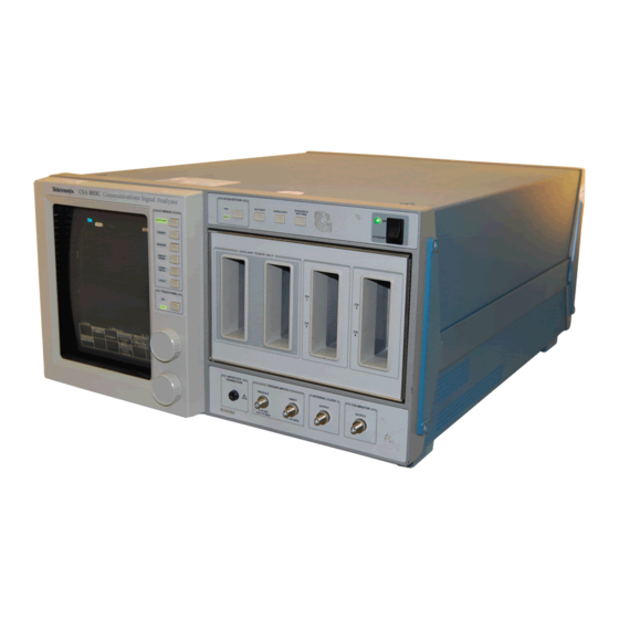
Tektronix CSA 803C Service Manual (280 pages)
Communications Signal Analyzer
Brand:
Tektronix
| Category:
Measuring Instruments
| Size: 2 MB
Table of Contents
Table of Contents
10
Table 1 1: Measurement Limits, Specifications, Adjustments, and Functional Tests
27
Figure 2 1: Sampling Head Compartments in the CSA 803C Communications Signal Analyzer
32
Figure 2 2: Power Cord Plug Identification
35
Table 2 1: Power Cord Conductor Identification
35
Address Latch
45
Function Decoder
45
Internal Clock Rate Generator
45
Data Buffers
45
Block Diagram Descriptions
45
A1 M/F Strobe Drive Board
45
Control Buffer
46
Voltage Fault Detect
46
A3 M/F Power Connect Board
46
A4 Regulator Board
46
A5 Time Base/Controller Board
46
Microprocessor
47
RAM/ROM Memory
47
Trigger
47
Figure 3 1: Trigger Edge Slew Rate for High Frequency Selection
48
Time Base
49
Acquisition System Interface
49
Red, Green, and Blue Video Amplifiers
50
Red, Green, and Blue Adjustments
50
Convergence Adjustment
50
Memory Management Unit (MMU) Interface
50
A7 CRT Socket Board
50
Horizontal Sweep
51
Vertical Sweep
51
High Voltage and Grid Voltage Generator
51
A8 CRT Driver Board
51
Touch Panel, Major Menu Keys, and Menu Status Leds
52
Degauss
52
Grid Bias
52
Beam Current Limit
52
A9, A10, and A11 Front Panel Boards
52
A9 Touch Panel Assembly
53
A10 Front Panel Control Board
53
A11 Front Panel Button Board
53
GPIB Data and Address Bus
54
A12 Rear Panel Assembly
54
Standard RS 232 C Controller
55
Printer Port
55
I/O Data Buffer
56
A13 Mother Board
56
A14 Input/Output (I/O) Board
56
I/O Delayed Data Buffer
57
Timer Configuration
57
Real Time Clock
57
Serial Data Interface (SDI)
57
Tone Generator
57
Temp/Tone Readback Buffer
57
Display Interface
58
A15 Memory Management Unit (MMU) Board
58
Waveform RAM
58
Mmu IC
58
Time Base/Controller Interface 3
59
Executive Processor (EXP) Interface
59
Display IC
59
Microprocessor
59
Bit Map RAM
59
Executive Processor (EXP)
60
Video Digital to Analog Converter (DAC)
60
Waveform Display RAM
60
A17 Executive Processor Board
60
Numeric Coprocessor
61
Bus Controller
61
Reset
61
Wait State
61
Interrupt Controllers
61
DMA Controller
61
Address Decode and Memory Select
62
Address Latches
62
A18 Memory Board
62
Eproms, SRAM, and NVRAM
63
Memory Data Buffers
63
Wait State Generator
63
Wait State Diagnostics
63
Memory Configuration Readback
63
Battery Backup
64
TDR Buffer and Level Shift
64
Strobe Sense Select
64
Strobe Deskew
64
A19 Strobe/Tdr Buffer Board
64
A20/A21 Head Interconnect (Power Only) Boards
65
A22/A23 Head Interconnect Boards
65
A26 M/F Acquisition Interconnect Board
65
Programmable Gain Amplifiers
66
A/D Converters
66
Measurement Hardware
66
A27 & A28 Acquisition System Boards
66
Time Base/Controller Interface
67
Shared RAM
67
Timing and Sampling Head Control
67
Performance Verification
69
Table 4 1: Measurement Limits, Specifications, and Functional Tests
69
Test Equipment
71
Table 4 2: Test Equipment
71
Test Record
74
Using These Procedures
79
Conventions in this Manual
79
Menu Selections and Measurement Techniques
79
User Manual
79
Performance Tests
81
Power on Diagnostics
82
Setup to Invoke Power on Diagnostics
82
Procedure to Invoke Power on Diagnostics
82
Diagnostics
83
Self Test Diagnostics
83
Power on Diagnostics Complete
84
Sampling Heads
85
Setup to Calibrate a Sampling Head
85
Procedure to Calibrate a Sampling Head
85
Extended Diagnostics
87
Setup to Invoke Extended Diagnostics
87
Procedure to Invoke Extended Diagnostics
87
Vertical Reference Voltage
89
Specifications
89
Setup to Check Vertical Reference Voltage
89
Procedure to Check Vertical Reference Voltage
89
Figure 4 1: A26 M/F Acquisition Interconnect Board Test Point
90
Horizontal Reference Clock
91
Specifications
91
Setup to Check Horizontal Reference Clock
91
Procedure to Check Horizontal Reference Clock
91
Figure 4 2: A5 Time Base/Controller Board Test Point Locations
92
Vertical Accuracy
93
Setup to Check Vertical Gain
93
Procedure to Check Vertical Gain
93
Table 4 3: Voltage Source Settings
95
Setup to Check Offset Accuracy
96
Procedure to Check Offset Accuracy
96
Table 4 4: Vertical Offset Test Values
98
System Vertical RMS Noise
99
Setup to Examine Vertical RMS Noise
99
Procedure to Examine Vertical RMS Noise
99
Table 4 5: Sensitivity Settings
101
Sweep Rate Accuracy
102
Setup to Examine Sweep Rate Accuracy
102
Procedure to Examine Sweep Rate Accuracy
102
Sweep Rate Accuracy 2 Ns/DIV
103
Sweep Rate Accuracy 1 Ns/DIV
104
Sweep Rate Accuracy 100 Ps/DIV
104
Sweep Rate Accuracy 10 Ps/DIV
104
Sweep Rate Accuracy 1 Ps/DIV
105
Triggering, External Direct
107
Specifications
107
Setup to Check Prescaler Triggering
107
Procedure to Check Prescaler Triggering
107
Prescaler Triggering
109
Specifications
109
Setup to Check Prescaler Triggering
109
Procedure to Check Prescaler Triggering
109
Table 4 6: Prescaler Test Settings
110
Internal Clock
111
Measurement Limits
111
Setup to Examine Internal Clock
111
Procedure to Examine Internal Clock
111
Calibrator Output
113
Measurement Limits
113
Setup to Examine Calibrator
113
Procedure to Examine Calibrator
113
Table 5 1: Measurement Limits and Adjustments
116
Table 5 2: Test Equipment
117
Test Equipment
117
Using These Procedures
120
Conventions in this Manual
120
Menu Selections and Measurement Techniques
120
User Manual
120
Power Supply
121
Measurement Limits
121
Setup to Examine Voltage Supply
121
Procedure to Examine Voltage Supply
121
Figure 5 1: A18 Memory Board Test Point Locations
122
Setup to Examine/Adjust Voltage Reference
123
Procedure to Examine/Adjust Voltage Reference
123
Figure 5 2: A2A2 Control Rectifier Board Test Point and
124
Setup to Examine/Adjust Regulator Reference
125
Procedure to Examine/Adjust Regulator Reference
125
Figure 5 3: A4 Regulator Board Test Point and Adjustment
126
Display
127
Measurement Limits
127
Setup to Examine/Adjust the Display
128
Procedure to Examine/Adjust the Display
128
Figure 5 4: A8 CRT Driver Board Adjustment Locations
132
Figure 5 5: A7 CRT Socket Board Adjustment Locations
133
Measurement Limits
134
Setup to Examine/Adjust Real Time Clock
134
Procedure to Examine/Adjust Real Time Clock
134
Figure 5 6: A14 I/O Board Test Point and Adjustment Locations
136
Real Time Clock
134
Preventive Maintenance
137
Removing the Cabinet Panel
137
Cleaning the Instrument
138
Exterior
138
Crt
138
Interior
139
Visual Inspection
139
Periodic Electrical Adjustment
139
Corrective Maintenance
141
Power Supply Voltage Hazard
141
Ordering Parts
141
Static Sensitive Device Classification
142
Table 6 1: Relative Susceptibility to Damage from Static Discharge
142
Removing and Replacing Frus
144
Table 6 2: FRU Removal/Replacement Figure Cross Reference
144
Electrical Lock on of the Front Panel ON/STANDBY Power Switch
149
Figure 6 1: Field Replaceable Units (FRU) Locator
150
Power Supply Module Removal/Replacement
152
Figure 6 2: Removing the Power Supply Module, Fan Housing, and Rear Panel Connector Plate
152
Figure 6 3: A2A2 Control Rectifier Board Connector Locations
153
Fan Motor Removal/Replacement
155
Cathode Ray Tube (CRT) Removal/Replacement
156
Figure 6 4: Removing/Replacing the CRT Cover
159
Figure 6 5: Removing/Replacing the Cathode Ray Tube
160
Figure 6 6: Removing/Replacing the CRT Torx Head Screws
161
Acquisition Unit Removal/Replacement
162
Battery Disposal and First Aid
163
Battery Disposal
163
Emergency and First Aid Information
164
Table 6 3: Emergency Procedures for Contact with Battery Solvent
164
FRU Board and Assembly Removal
165
Figure 6 7: Top View of the Card Cage
166
A1 M/F Strobe Drive Board
167
Figure 6 8: Removing/Replacing the A1 M/F Strobe Drive Board
167
A3 M/F Power Connect Board
168
A4 Regulator Board
169
Figure 6 9: Removing/Replacing the A4 Regulator Board
170
A5 Time Base/Controller Board
171
Figure 6 10: Removing/Replacing the A5 Time Base/Controller
172
A7 CRT Socket Board and A8 CRT Driver Board
173
Figure 6 11: Removing/Replacing the A7 CRT Socket Board
174
Figure 6 12: Removing/Replacing the A8 CRT Driver Board
175
A9 Touch Panel Assembly
176
Figure 6 13: A9 Touch Panel Assembly Torx Head Screws
177
Figure 6 14: Removing/Replacing the A9 Touch Panel Assembly
177
A10 Front Panel Control Board
178
Figure 6 15: Removing/Replacing the A10 Front Panel Control Board
179
A11 Front Panel Button Board
180
Figure 6 16: Removing/Replacing the A11 Front Panel Button Board
180
A12 Rear Panel Assembly
181
Figure 6 17: Removing/Replacing the A12 Rear Panel Assembly
182
A13 Mother Board
183
Figure 6 18: Removing/Replacing the A13 Mother Board
184
A14 Input/Output (I/O) Board
185
Figure 6 19: Removing/Replacing the A14 I/O Board
186
A15 Memory Management Unit (MMU) Board
187
Figure 6 20: Removing/Replacing the A15 MMU Board
188
A17 Executive Processor (EXP) Board
189
Figure 6 21: Removing/Replacing the A17 Executive Processor
190
A18 Memory Board
191
Figure 6 22: Removing/Replacing the A18 Memory Board
192
A19 Strobe/Tdr Buffer Board
193
Figure 6 23: Removing/Replacing the A19 Strobe/Tdr Buffer
194
A20/A21 Head Interconnect (Power Only) and A22/A23 Head Lnterconnect Boards
195
Figure 6 24: Removing/Replacing the A20/A21 Head Interconnect (Power Only) and the A22/A23 Head Interconnect Boards
196
Figure 6 25: Removing/Replacing the Front Subpanel Assembly
197
A26 M/F Acquisition Lnterconnect Board
198
Figure 6 26: Removing/Replacing the A26 M/F Acquisition Interconnect Board
198
Figure 6 27: Top View of the A26 Mainframe Acquisition
199
A27 Acquisition Analog Board
200
Figure 6 28: Removing/Replacing the A27 Acquisition Analog Board
200
A28 Acquisition MPU Board
201
Figure 6 29: Removing/Replacing the A28 Acquisition MPU Board
201
FRU IC Removal
202
Serial Data Interface Integrated Circuits (Slam Pack" Ics)
202
Figure 6 30: FRU IC Detail
204
Firmware Integrated Circuits (Dual in Line Package" Ics)
205
Firmware Upgrade Procedure
205
Figure 6 31: IC Insertion Extraction Tool
207
Figure 6 32: Multi Pin Connector Orientation and Semiconductor
210
Cables and Connectors
211
Interconnecting Pins
211
Coaxial Type End Lead Connectors
211
Multi Pin Connectors
211
Checks after FRU Replacement
213
Table 6 4: Checks Required after FRU Replacement
213
Diagnostic Troubleshooting
215
Diagnostics Overview
215
Kernel Diagnostics
216
Self Test/Extended Diagnostics
217
Extended Diagnostics Menu Structure
217
Extended Diagnostics Error Index Codes
217
Table 6 5: Extended Diagnostics Error Index Code Descriptions
218
Diagnostic Menus
220
Diagnostic Menu Hardcopy
221
Diagnostic Terminal Mode
222
System Mode (GPIB & RS 232 C)
223
Table 6 6: System Mode Commands
223
Table 6 7: Event Code Descriptions
223
Battery Testing
225
Clearing NVRAM
226
Field Replaceable Unit (FRU) Guide
226
FRU Name Abbreviations
227
Table 6 8: Board Frus
227
Component and Module Name Abbreviations
228
Table 6 9: Component Module Frus
228
Executive Subsystem Error Codes
229
Table 6 10: Executive Processor Kernel Error Index Codes
229
Figure 6 33: A17 Executive Processor Board Test Point and
230
Table 6 11: Executive Processor Status LED Configuration
230
Table 6 12: Executive Processor Manual Tests
231
Display Subsystem Error Index Codes
233
Table 6 13: Display Processor Kernel Error Index Codes
233
Table 6 14: Display Processor Status LED Configuration
233
Time Base Processor Error Index Codes
234
Figure 6 34: A15 MMU Board Test Point and Status
234
Table 6 15: Time Base Processor Kernel Error Index Codes
234
Figure 6 35: A5 Time Base/Controller Board Status Leds
235
Acquisition Processor Error Index Codes
236
Figure 6 36: A28 Acquisition MPU Board Status Leds
236
Table 6 16: Acquisition Processor Kernel Error Index Codes
236
Other Troubleshooting
237
Power Supply Module
237
Module Troubleshooting
237
A4 Regulator Board
237
CRT, A7 CRT Socket Board, or A8 CRT Driver Board
238
Module Troubleshooting
238
A13 Mother Board
238
Fuse Testing
239
Table 6 17: A14 I/O Board Fuse Failures
240
Figure 6 37: A14 I/O Board Fuse Locator Diagram
241
Time Base Calibration Errors
242
Table 6 18: Time Base Calibration Errors
243
Acquisition Calibration Errors
244
Figure 7 1: Power Cord Plug Identification
246
Table 7 1: Power Cord Conductor Identification
246
Figure 9 1: CSA 803C System Functional Block Diagram
249
Figure 9 2: A1 M/F Strobe Drive Board Block Diagram
249
Figure 9 3: A4 Regulator Board Block Diagram
250
Figure 9 4: A5 Time Base/Controller Board Block Diagram
250
Figure 9 5: A7 CRT Socket Board Block Diagram
250
Figure 9 6: A8 CRT Driver Board Block Diagram
251
Figure 9 7: A12 Rear Panel Assembly Block Diagram
251
Figure 9 8: A14 I/O Board Block Diagram
252
Figure 9 9: A15 MMU Board Block Diagram
252
Figure 9 10: A17 Executive Processor Board Block Diagram
252
Figure 9 11: A18 Memory Board Block Diagram
253
Figure 9 12: A19 Strobe/Tdr Buffer Board Block Diagram
253
Figure 9 13: A26 M/F Acquisition Interconnect Board Block
253
Figure 9 14: A27 Acquisition Analog Board Block Diagram
254
Figure 9 15: A28 Acquisition MPU Board Block Diagram
254
Table 10 1: Board Frus
263
Figure 10 1: Cabinet
267
Figure 10 2: Front Panel
269
Figure 10 3: Chassis, Rear
271
Figure 10 4: Circuit Boards
273
Figure 10 5: Acquisition Module
276
Figure 10 6: Power Supply
278
Figure 10 7: Accessories
280
Advertisement
Advertisement
Related Products
Tektronix CSA7404
Tektronix CSA7154
Tektronix CSA7404B
Tektronix CSA 803A
Tektronix CDC250
Tektronix CM-9930
Tektronix CSA8000B Series
Tektronix CSA8200 Series
Tektronix CSA8000 Series
Tektronix CSA 907A
Tektronix Categories
Test Equipment
Measuring Instruments
Amplifier
Portable Generator
Printer
More Tektronix Manuals
Login
Sign In
OR
Sign in with Facebook
Sign in with Google
Upload manual
Upload from disk
Upload from URL