Sign In
Upload
Manuals
Brands
rtd Manuals
Computer Hardware
FPGA35S6045HR
rtd FPGA35S6045HR Xilinx Spartan-6 FPGA Manuals
Manuals and User Guides for rtd FPGA35S6045HR Xilinx Spartan-6 FPGA. We have
1
rtd FPGA35S6045HR Xilinx Spartan-6 FPGA manual available for free PDF download: User Manual
Rtd FPGA35S6045HR User Manual (31 pages)
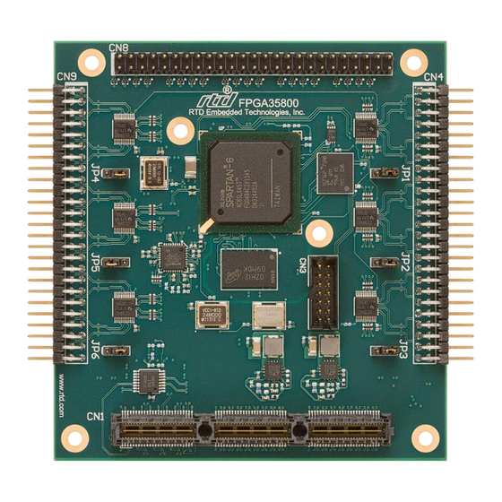
FPGA Module
Brand:
Rtd
| Category:
Computer Hardware
| Size: 1 MB
Table of Contents
Revision History
3
Table of Contents
4
1 Introduction
7
Product Overview
7
Board Features
7
Ordering Information
8
Contact Information
8
Sales Support
8
Technical Support
8
Table 1: Ordering Options
8
2 Specifications
9
Operating Conditions
9
Electrical Characteristics
9
Table 2: Operating Conditions
9
Table 3: Electrical Characteristics
9
3 Board Connection
10
Board Handling Precautions
10
Physical Characteristics
10
Figure 1: Board Dimensions
10
Connectors and Jumpers
11
Figure 2: Board Connections
11
External I/O Connectors
12
CN3: Xilinx JTAG Programming Header
12
Figure 3: Bottom Solder Jumper Locations
12
Table 4: CN3 Programming Header
12
CN8: High Speed Digital I/O Connector
13
Table 5: CN8 I/O Pin Assignments
13
CN4 & CN9: Digital I/O Connector
14
Bus Connectors
14
CN1 (Top) & CN2 (Bottom): Pcie Connector
14
Jumpers
14
JP1, JP2, JP3, JP4, JP5, & JP6: Pull Up/Pull down Jumper
14
Table 6: CN4 I/O Pin Assignments
14
Table 7: CN9 I/O Pin Assignments
14
Table 8: Pull Up/Pull down Jumper Options
14
JP7: Reserved
15
Solder Jumper
15
B1: Pull up Voltage
15
B2: Pull up Voltage
15
Table 9: B1 Pull up Voltage
15
Table 10: B2 Pull up Voltage
15
Steps for Installing
16
Figure 4: Example 104™Stack
16
4 IDAN Connections
17
Module Handling Precautions
17
Physical Characteristics
17
Figure 5: IDAN Dimensions
17
Connectors and Jumpers
18
P2 & P3: Digital I/O Connector
18
Table 11: P2 and P3 Pin Assignments
18
P4: High Speed Digital I/O Connector
19
Table 12: P4 Pin Assignments
19
Bus Connectors
21
CN1 (Top) & CN2 (Bottom): Pcie Connector
21
Jumpers
21
JP1, JP2, JP3, JP4, JP5, & JP6: Pull Up/Pull down Jumper
21
JP7: Reserved
21
Solder Jumper
21
B1: Pull up Voltage
21
B2: Pull up Voltage
21
Table 13: Pull Up/Pull down Jumper Options
21
Table 14: B1 Pull up Voltage
21
Steps for Installing
22
Figure 6: Example IDAN System
22
5 Functional Description
23
Oscillator
23
Eeprom
23
Ddr2 Sram
23
Figure 7: FPGA35S6 Block Diagram
23
Digital I/O
24
Figure 8: CN4/CN9 Digital I/O Circuitry
24
6 Register Address Space
25
BAR0 - FPGA Example Register Map
25
R_ID (Read)
25
R_STATUS (Read)
25
R_EEPROM (Read/Write)
25
Table 16: FPGA Example Register Map
25
R_PORT0_IN (Read)
26
R_PORT0_OUT (Write)
26
R_PORT0_DIR (Write)
26
R_PORT1_IN (Read)
26
R_PORT1_OUT (Write)
26
R_PORT1_DIR (Read/Write)
26
R_PORT2L_IN (Read)
26
R_PORT2L_OUT (Write)
26
R_PORT2L_DIR (Read/Write)
26
R_PORT2H_IN (Read)
26
R_DDR_STATUS (Read)
27
7 Troubleshooting
28
8 Additional Information
29
PC/104 Specifications
29
PCI and PCI Express Specification
29
9 Limited Warranty
30
Advertisement
Advertisement
Related Products
rtd FPGA35S6100HR
rtd FPGA35S6 Series
rtd FPGA35S6046HR
rtd FPGA35S6101HR
rtd BDM-610000049
rtd CAN SPIDER
rtd CMA34KB
rtd CMi37786HX
RTD CMV6486DX100HR
RTD CMV6486DX66HR
rtd Categories
Computer Hardware
Control Unit
PCI Card
Switch
GPS
More rtd Manuals
Login
Sign In
OR
Sign in with Facebook
Sign in with Google
Upload manual
Upload from disk
Upload from URL