Sign In
Upload
Manuals
Brands
NXP Semiconductors Manuals
Computer Hardware
MCF5272 ColdFire
NXP Semiconductors MCF5272 ColdFire Manuals
Manuals and User Guides for NXP Semiconductors MCF5272 ColdFire. We have
1
NXP Semiconductors MCF5272 ColdFire manual available for free PDF download: User Manual
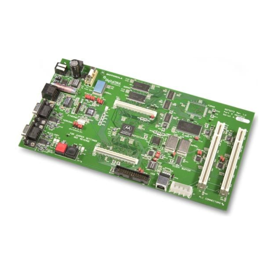
NXP Semiconductors MCF5272 ColdFire User Manual (545 pages)
Brand:
NXP Semiconductors
| Category:
Computer Hardware
| Size: 5 MB
Table of Contents
Table of Contents
5
Paragraph Page
14
MCF5272 Coldfire ® Integrated Microprocessor User's Manual
38
Overview
40
General Information
43
Acronyms and Abbreviations
45
MCF5272 Key Features
61
MCF5272 Block Diagram
62
MCF5272 Architecture
64
Version 2 Coldfire Core
64
System Integration Module (SIM)
65
Number
14
Chapter 1
65
External Bus Interface
65
Chip Select and Wait State Generation
65
System Configuration and Protection
65
Power Management
66
Parallel Input/Output Ports
66
Interrupt Inputs
66
UART Module
66
Timer Module
67
Test Access Port
67
System Design
67
System Bus Configuration
67
MCF5272-Specific Features
67
Physical Layer Interface Controller (PLIC)
67
Pulse-Width Modulation (PWM) Unit
68
Queued Serial Peripheral Interface (QSPI)
68
Universal Serial Bus (USB) Module
68
Coldfire Core
69
Features and Enhancements
69
Decoupled Pipelines
69
Instruction Fetch Pipeline (IFP)
70
Operand Execution Pipeline (OEP)
70
Coldfire Pipeline
70
Illegal Opcode Handling
71
Hardware Multiply/Accumulate (MAC) Unit
71
Coldfire Multiply-Accumulate Functionality Diagram
71
Hardware Divide Unit
72
Debug Module Enhancements
72
Programming Model
72
User Programming Model
72
Address Registers (A0-A6)
73
Data Registers (D0-D7)
73
MCF5272 Coldfire Integrated Microprocessor User's Manual, Rev
73
Stack Pointer (A7, SP)
73
Coldfire Programming Model
73
Program Counter (PC)
74
Condition Code Register (CCR)
74
MAC Programming Model
75
Supervisor Programming Model
75
Status Register (SR)
76
Vector Base Register (VBR)
76
Access Control Registers (ACR0-ACR1)
77
Cache Control Register (CACR)
77
Module Base Address Register (MBAR)
77
RAM Base Address Register (RAMBAR)
77
ROM Base Address Register (ROMBAR)
77
Integer Data Formats
77
Organization of Data in Registers
78
Organization of Integer Data Formats in Registers
78
Organization of Integer Data Formats in Memory
79
Memory Operand Addressing
79
Addressing Mode Summary
80
Instruction Set Summary
81
Supervisor-Mode Instruction Set Summary
86
Instruction Timing
87
MOVE Instruction Execution Times
88
Move Long Execution Times
89
Execution Timings-One-Operand Instructions
90
Execution Timings-Two-Operand Instructions
90
Miscellaneous Instruction Execution Times
92
Branch Instruction Execution Times
93
Exception Processing Overview
93
Exception Vector Assignments
94
Exception Stack Frame Definition
95
Processor Exceptions
96
Chapter 3 Hardware Multiply/Accumulate (MAC) Unit
99
Overview
99
Coldfire MAC Multiplication and Accumulation
99
MAC Programming Model
100
General Operation
101
MAC Instruction Set Summary
102
Data Representation
102
MAC Instruction Execution Timings
102
Chapter 4 Local Memory
103
Interactions between Local Memory Modules
103
Local Memory Registers
104
SRAM Overview
104
SRAM Operation
104
SRAM Programming Model
104
SRAM Base Address Register (RAMBAR)
105
Programming RAMBAR for Power Management
106
SRAM Initialization
106
ROM Overview
107
ROM Operation
107
ROM Programming Model
107
ROM Base Address Register (ROMBAR)
107
Programming ROMBAR for Power Management
108
Instruction Cache Overview
109
Instruction Cache Physical Organization
109
Instruction Cache Operation
110
Cache Coherency and Invalidation
110
Interaction with Other Modules
110
Instruction Cache Block Diagram
110
Caching Modes
111
Cache-Inhibited Accesses
111
Cacheable Accesses
111
Cache Miss Fetch Algorithm/Line Fills
112
Reset
112
Instruction Cache Operation as Defined by CACR[CENB,CEIB]
113
Instruction Cache Programming Model
114
Cache Control Register (CACR)
114
CACR Field Descriptions
115
Access Control Registers (ACR0 and ACR1)
116
Access Control Register Format (Acrn)
116
Chapter 5 Debug Support
119
Overview
119
Processor/Debug Module Interface
119
Signal Description
120
PSTCLK Timing
120
Real-Time Trace Support
121
Begin Execution of Taken Branch (PST = 0X5)
122
Programming Model
123
Example JMP Instruction Output on PST/DDATA
123
Debug Programming Model
124
Revision a Shared Debug Resources
125
Address Attribute Trigger Register (AATR)
125
Address Breakpoint Registers (ABLR, ABHR)
127
Configuration/Status Register (CSR)
128
Data Breakpoint/Mask Registers (DBR, DBMR)
130
Program Counter Breakpoint/Mask Registers (PBR, PBMR)
131
Program Counter Breakpoint Register (PBR)
131
Trigger Definition Register (TDR)
132
Background Debug Mode (BDM)
133
CPU Halt
134
BDM Serial Interface
135
Receive Packet Format
136
Transmit Packet Format
136
Receive BDM Packet
136
BDM Command Set
137
Coldfire BDM Command Format
138
Extension Words as Required
138
Command Sequence Diagrams
139
Command Set Descriptions
140
Read A/D Register ( RAREG / RDREG )
140
WAREG / WDREG Command Format
141
Write A/D Register ( WAREG / WDREG )
141
Read Memory Location ( READ )
142
WRITE Command Format
143
Write Memory Location ( WRITE )
143
WRITE Command Sequence
144
Dump Memory Block ( DUMP )
145
Fill Memory Block ( FILL )
146
Resume Execution ( GO )
147
No Operation ( NOP )
148
NOP Command Format
148
Read Control Register ( RCREG )
148
Write Control Register ( WCREG )
149
Definition of Drc Encoding—Read
150
Read Debug Module Register ( RDMREG )
150
Write Debug Module Register ( WDMREG )
151
Real-Time Debug Support
151
WDMREG BDM Command Format
151
Theory of Operation
152
Emulator Mode
153
Concurrent BDM and Processor Operation
153
Processor Status, DDATA Definition
154
User Instruction Set
154
PST/DDATA Specification for User-Mode Instructions
155
Supervisor Instruction Set
158
Freescale-Recommended BDM Pinout
159
Recommended BDM Connector
159
Chapter 6 System Integration Module (SIM)
161
Features
161
SIM Block Diagram
161
Programming Model
162
SIM Register Memory Map
162
Module Base Address Register (MBAR)
163
Module Base Address Register (MBAR)
164
System Configuration Register (SCR)
165
System Protection Register (SPR)
166
Power Management Register (PMR)
167
Timer Module
168
USB and USART Power down Modes
169
Activate Low-Power Register (ALPR)
170
Device Identification Register (DIR)
171
Software Watchdog Timer
171
Watchdog Interrupt Reference Register (WIRR)
172
Watchdog Reset Reference Register (WRRR)
172
Watchdog Counter Register (WCR)
173
Watchdog Event Register (WER)
173
Chapter 7 Interrupt Controller
175
Overview
175
Interrupt Controller Registers
176
Interrupt Controller Block Diagram
176
Chapter 2 Coldfire Core
177
Interrupt Control Registers (ICR1-ICR4)
178
Interrupt Control Register 1 (ICR1)
178
Interrupt Control Register 2 (ICR2)
179
Interrupt Control Register 3 (ICR3)
179
Interrupt Control Register 4 (ICR4)
179
Interrupt Source Register (ISR)
180
Programmable Interrupt Transition Register (PITR)
181
Programmable Interrupt Wakeup Register (PIWR)
182
Programmable Interrupt Vector Register (PIVR)
183
MCF5272 Interrupt Vector Table
184
Chapter 8 Chip Select Module
185
Overview
185
Features
185
Chip Select Usage
185
Boot CS0 Operation
186
Chip Select Registers
186
Chip Select Base Registers (CSBR0-CSBR7)
187
Output Read/Write Strobe Levels Versus Chip Select EBI Code
188
Chip Select Option Registers (CSOR0-CSOR7)
189
Chapter 9 SDRAM Controller
191
Overview
191
SDRAM Controller Signals
191
Pin TSOP SDRAM Pin Definition
193
Interface to SDRAM Devices
194
Internal Address Multiplexing (16-Bit Data Bus)
195
SDRAM Banks, Page Hits, and
196
SDRAM Registers
196
SDRAM Configuration Register (SDCR)
196
SDCR Field Descriptions
197
SDRAM Timing Register (SDTR)
198
Auto Initialization
199
Power-Down and Self-Refresh
199
Performance
200
SDRAM Controller Performance (RCD = 1, RP = 1), 16-Bit Port
201
Solving Timing Issues with SDCR[INV]
202
Example Setup Time Violation on SDRAM Data Input During Write
202
Timing Refinement with Inverted SDCLK
203
SDRAM Interface
204
Timing Refinement with Effective cas Latency
204
SDRAM Read Accesses
205
SDRAM Burst Read, 32-Bit Port, Page Miss, Access = 9-1-1-1
206
SDRAM Burst Read, 32-Bit Port, Page Hit, Access = 5-1-1-1
207
SDRAM Write Accesses
208
SDRAM Burst Write, 32-Bit Port, Page Miss, Access = 7-1-1-1
208
SDRAM Burst Write, 32-Bit Port, Page Hit, Access = 3-1-1-1
209
SDRAM Refresh Timing
210
SDRAM Refresh Cycle
210
Enter SDRAM Self-Refresh Mode
211
Exit SDRAM Self-Refresh Mode
212
Chapter 10 DMA Controller
213
DMA Data Transfer Types
213
DMA Address Modes
214
DMA Controller Registers
214
DMA Mode Register (DMR)
214
DMA Interrupt Register (DIR)
216
DMA Source Address Register (DSAR)
217
DMA Destination Address Register (DDAR)
218
DMA Byte Count Register (DBCR)
218
Ethernet Module
219
Overview
219
Features
219
Module Operation
219
Ethernet Block Diagram
220
Transceiver Connection
221
FEC Frame Transmission
222
Ethernet Frame Format
222
FEC Frame Reception
223
CAM Interface
224
Ethernet Address Recognition
224
Ethernet Address Recognition Flowchart
225
Hash Table Algorithm
226
Interpacket Gap Time
226
Collision Handling
226
Internal and External Loopback
226
Ethernet Error-Handling Procedure
227
Reception Errors
227
Transmission Errors
227
Programming Model
228
Ethernet Control Register (ECR)
229
Interrupt Event Register (EIR)
230
Interrupt Mask Register (EIMR)
231
Interrupt Vector Status Register (IVSR)
232
Receive Descriptor Active Register (RDAR)
233
Transmit Descriptor Active Register (TDAR)
234
MII Management Frame Register (MMFR)
235
MII Speed Control Register (MSCR)
236
FIFO Receive Bound Register (FRBR)
237
FIFO Receive Start Register (FRSR)
238
Transmit FIFO Watermark (TFWR)
239
FIFO Transmit Start Register (TFSR)
240
Receive Control Register (RCR)
241
Maximum Frame Length Register (MFLR)
242
Transmit Control Register (TCR)
243
RAM Perfect Match Address Low (MALR)
244
RAM Perfect Match Address High (MAUR)
245
Hash Table High (HTUR)
246
Hash Table Low (HTLR)
247
Pointer-To-Receive Descriptor Ring (ERDSR)
248
Pointer-To-Transmit Descriptor Ring (ETDSR)
249
Receive Buffer Size Register (EMRBR)
250
11.5.22 Initialization Sequence
251
11.5.22.1 Hardware Initialization
251
User Initialization (Prior to Asserting ETHER_EN)
251
11.5.24 FEC Initialization
252
User Initialization (after Setting ETHER_EN)
252
Buffer Descriptors
252
FEC Buffer Descriptor Tables
253
Ethernet Receive Buffer Descriptor (Rxbd)
253
Rxbd Field Descriptions
254
Ethernet Transmit Buffer Descriptor
255
Differences between MCF5272 FEC and MPC860T FEC
257
Chapter 12 Universal Serial Bus (USB)
259
Introduction
259
Module Operation
260
USB Module Architecture
260
The USB "Tiered Star" Topology
260
USB Transceiver Interface
261
USB Module Block Diagram
261
Clock Generator
262
USB Control Logic
262
Endpoint Controllers
263
USB Request Processor
263
Register Description and Programming Model
265
USB Memory Map
265
Register Descriptions
267
USB Frame Number Match Register (FNMR)
267
USB Frame Number Register (FNR)
267
USB Real-Time Frame Monitor Register (RFMR)
268
USB Function Address Register (FAR)
269
USB Real-Time Frame Monitor Match Register (RFMMR)
269
USB Alternate Settings Register (ASR)
270
USB Device Request Data 1 and 2 Registers (DRR1/ 2)
271
USB Device Request Data 1 Register (DRR1)
271
USB Specification Number Register (SPECR)
272
USB Endpoint 0 Status Register (EP0SR)
272
USB Endpoint 0 in Configuration Register (IEP0CFG)
273
USB Endpoint 0 out Configuration Register (OEP0CFG)
274
USB Endpoint 1-7 Configuration Register (Epncfg)
274
USB Endpoint 0 Control Register (EP0CTL)
275
USB Endpoint 1-7 Control Register (Epnctl)
278
Registers (EP0ISR)
280
USB Endpoint 0 Interrupt Mask (EP0IMR and General/Endpoint 0 Interrupt Registers (EP0ISR)
280
USB Endpoints 1-7 Status / Interrupt Registers (Epnisr)
283
USB Endpoint 1-7 Interrupt Mask Registers (Epnimr)
284
USB Endpoint 0-7 Data Registers (Epndr)
285
USB Endpoint 0-7 Data Present Registers (Epndpr)
286
Configuration RAM
286
Configuration RAM Content
286
USB Device Configuration Example
287
Example USB Configuration Descriptor Structure
287
USB Module Access Times
288
Configuration RAM
288
Endpoint Fifos
288
Registers
288
Software Architecture and Application Notes
289
USB Module Initialization
289
USB Configuration and Interface Changes
289
FIFO Configuration
290
Data Flow
290
Control, Bulk, and Interrupt Endpoints
291
IN Endpoints
291
Isochronous Endpoints
291
OUT Endpoints
291
IN Endpoints
292
OUT Endpoints
292
Class- and Vendor-Specific Request Operation
292
Endpoint Halt Feature
293
Line Interface
294
Attachment Detection
294
PCB Layout Recommendations
294
Recommended USB Line Interface
294
Recommended USB Protection Circuit
295
Chapter 13 Physical Layer Interface Controller (PLIC)
297
Introduction
297
PLIC System Diagram
298
GCI/IDL Block
299
GCI/IDL B- and D-Channel Receive Data Registers
299
GCI/IDL B- and D-Channel Transmit Data Registers
300
GCI/IDL B-Channel Receive Data Register Demultiplexing
300
GCI/IDL B- and D-Channel Bit Alignment
301
B-Channel Unencoded Data
301
GCI/IDL B Data Transmit Register Multiplexing
301
B-Channel HDLC Encoded Data
302
D-Channel HDLC Encoded Data
302
B-Channel Unencoded and HDLC Encoded Data
302
D-Channel Unencoded Data
303
D-Channel HDLC Encoded and Unencoded Data
303
GCI/IDL D-Channel Contention
304
GCI/IDL Looping Modes
304
Automatic Echo Mode
305
Local Loopback Mode
305
Remote Loopback Mode
305
GCI/IDL Interrupts
305
GCI/IDL Periodic Frame Interrupt
305
GCI/IDL Loopback Mode
305
GCI Aperiodic Status Interrupt
306
Periodic Frame Interrupt
306
Interrupt Control
307
PLIC Timing Generator
307
Clock Synthesis
307
PLIC Internal Timing Signal Routing
308
Super Frame Sync Generation
309
Frame Sync Synthesis
309
PLIC Register Memory Map
309
PLIC Registers
311
B1 Data Receive Registers (P0B1RR-P3B1RR)
311
B2 Data Receive Registers (P0B2RR-P3B2RR)
312
D Data Receive Registers (P0DRR-P3DRR)
312
B2 Receive Data Registers P0B2RR – P3B2RR
312
B1 Data Transmit Registers (P0B1TR-P3B1TR)
313
B2 Data Transmit Registers (P0B2TR-P3B2TR)
313
D Data Transmit Registers (P0DTR-P3DTR)
314
Port Configuration Registers (P0CR-P3CR)
314
P0CR–P3CR Field Descriptions
315
Loopback Control Register (PLCR)
316
Interrupt Configuration Registers (P0ICR-P3ICR)
316
P0ICR–P3ICR Field Descriptions
317
Periodic Status Registers (P0PSR-P3PSR)
318
Aperiodic Status Register (PASR)
319
GCI Monitor Channel Receive Registers (P0GMR-P3GMR)
320
GCI Monitor Channel Transmit Registers (P0GMT-P3GMT)
321
GCI Monitor Channel Transmit Abort Register
322
GCI Monitor Channel Transmit Status Register
323
GCI C/I Channel Receive Registers (P0GCIR-P3GCIR)
324
GCI C/I Channel Transmit Registers (P0GCIT-P3GCIT)
325
GCI C/I Channel Transmit Status Register
326
D-Channel Status Register (PDCSR)
327
D-Channel Request Register (PDRQR)
328
Sync Delay Registers (P0SDR-P3SDR)
329
Clock Select Register (PCSR)
330
Application Examples
331
Introduction
331
PLIC Initialization
331
Port Configuration Example
331
Port 1 Configuration Register (P1CR)
332
Interrupt Configuration Example
333
Port 1 Interrupt Configuration Register (P1ICR)
333
Example 1: ISDN SOHO PBX with Ports 0, 1, 2, and 3
334
Standard IDL2 10-Bit Mode
335
Example 2: ISDN SOHO PBX with Ports 1, 2, and 3
336
Standard IDL2 10-Bit Mode
337
Standard IDL2 8-Bit Mode
338
Chapter 14 Queued Serial Peripheral Interface (QSPI) Module
339
Overview
339
Features
339
Module Description
339
QSPI Block Diagram
340
Interface and Pins
341
Internal Bus Interface
341
Operation
341
Qspi Ram
342
QSPI RAM Model
343
Receive RAM
343
Command RAM
344
Transmit RAM
344
Baud Rate Selection
344
Transfer Delays
345
Transfer Length
346
Data Transfer
346
Programming Model
347
QSPI Mode Register (QMR)
347
QSPI Clocking and Data Transfer Example
348
QSPI Delay Register (QDLYR)
349
SPI Modes Timing
349
QSPI Wrap Register (QWR)
350
QSPI Interrupt Register (QIR)
351
QSPI Address Register (QAR)
352
QSPI Data Register (QDR)
352
Command RAM Registers (QCR0-QCR15)
353
Programming Example
354
Chapter 15 Timer Module
355
Overview
355
Timer Operation
355
Timer Block Diagram
356
General-Purpose Timer Registers
357
Timer Mode Registers (TMR0-TMR3)
357
Timer Reference Registers (TRR0-TRR3)
358
Timer Capture Registers (TCAP0-TCAP3)
358
Timer Counters (TCN0-TCN3)
358
Timer Event Registers (TER0-TER3)
359
Chapter 16 UART Modules
361
Overview
361
System Integration Module (SIM
361
Serial Module Overview
362
Register Descriptions
362
UART Module Programming Model
363
UART Mode Registers 1 (Umr1N)
364
Umr1N Field Descriptions
365
UART Mode Register 2 (Umr2N)
366
UART Status Registers (Usrn)
367
UART Clock-Select Registers (Ucsrn)
368
UART Command Registers (Ucrn)
369
UART Receiver Buffers (Urbn)
370
UART Transmitter Buffers (Utbn)
371
UART Input Port Change Registers (Uipcrn)
371
UART Auxiliary Control Registers (Uacrn)
372
UART Interrupt Status/Mask Registers (Uisrn/Uimrn)
372
UART Interrupt Status/Mask Registers (Uisrn/Uimrn)
373
UART Divider Upper/Lower Registers (Udun/Udln)
374
UART Autobaud Registers (Uabun/Uabln)
374
UART Transmitter FIFO Registers (Utfn)
375
UART Receiver FIFO Registers (Urfn)
376
UART Fractional Precision Divider Control Registers (Ufpdn)
377
UART Input Port Registers (Uipn)
377
UART Output Port Command Registers (Uop1N/Uop0N)
378
UART Module Signal Definitions
378
Interrupt Controller
378
Operation
379
Transmitter/Receiver Clock Source
379
UART/RS-232 Interface
379
Programmable Divider
380
Calculating Baud Rates
380
CLKIN Baud Rates
380
Clocking Source Diagram
380
External Clock
381
Autobaud Detection
381
Transmitter and Receiver Operating Modes
382
Transmitting
382
Transmitter and Receiver Functional Diagram
382
Transmitter Timing
383
Receiver
384
Receiver Timing
384
Transmitter FIFO
385
Receiver FIFO
385
Looping Modes
386
Automatic Echo Mode
387
Local Loop-Back Mode
387
Remote Loop-Back Mode
387
Multidrop Mode
388
Remote Loop-Back
388
Bus Operation
389
Interrupt Acknowledge Cycles
389
Multidrop Mode Timing Diagram
389
Read Cycles
389
Write Cycles
389
Programming
390
UART Module Initialization Sequence
390
UART Mode Programming Flowchart (Sheet 1 of 5)
390
Chapter 17 General Purpose I/O Module
395
Overview
395
Port Control Registers
396
Port a Control Register (PACNT)
397
Port B Control Register (PBCNT)
399
PBCNT Field Descriptions
400
Port B Control Register Function Bits
401
Port C Control Register
402
Port D Control Register (PDCNT)
402
Port D Control Register Function Bits
403
Data Direction Registers
404
Port a Data Direction Register (PADDR)
404
Port B Data Direction Register (PBDDR)
404
Port C Data Direction Register (PCDDR)
405
Port Data Registers
405
Port Data Register (Pxdat)
405
Chapter 18 Pulse-Width Modulation (PWM) Module
407
Overview
407
PWM Block Diagram (3 Identical Modules)
407
PWM Operation
408
PWM Programming Model
408
PWM Control Register (Pwcrn)
409
PWM Width Register (Pwwdn)
410
Chapter 19 Signal Descriptions
411
MCF5272 Block Diagram with Signal Interfaces
411
MCF5272 Block Diagram with Signal Interfaces
412
Signal List
413
Signal Name and Description by Pin Number
421
Address Bus (A[22:0]/SDA[13:0])
429
Data Bus (D[31:0])
429
Dynamic Data Bus Sizing
429
Chip Selects (CS7/SDCS, CS[6:0])
429
SDRAM Controller
429
Bus Control Signals
430
Output Enable/Read (OE/RD)
430
Byte Strobes (BS[3:0])
430
Read/Write (R/W)
431
Transfer Acknowledge (TA/PB5)
432
Hi-Z
432
Bypass
432
SDRAM Row Address Strobe (RAS0)
432
SDRAM Column Address Strobe (CAS0)
432
SDRAM Clock (SDCLK)
432
SDRAM Write Enable (SDWE)
432
SDRAM Clock Enable (SDCLKE)
432
SDRAM Bank Selects (SDBA[1:0])
433
SDRAM Row Address 10 (A10)/A10 Precharge (A10_PRECHG)
433
CPU Clock and Reset Signals
433
Rsti
433
Dreseten
433
CPU External Clock (CLKIN)
433
Reset Output (RSTO)
433
Interrupt Request Inputs (INT[6:1])
433
General-Purpose I/O (GPIO) Ports
434
UART0 Module Signals and PB[4:0]
434
Transmit Serial Data Output (Urt0_Txd/Pb0)
434
Clock (URT0_CLK/PB4)
435
Receive Serial Data Input (Urt0_Rxd/Pb1)
435
USB Transmit Data Negative (USB_TN/PA3)
436
19.12 Timer Module Signals
437
Timer Input 0 (TIN0)
437
19.12.2 Timer Output (TOUT0)/PB7
437
Timer Input 1 (TIN1)/PWM Mode Output 2 (PWM_OUT2)
437
Timer Output 1 (TOUT1)/PWM Mode Output 1 (PWM_OUT1)
437
Chapter 11 Ethernet Module
437
Collision (E_COL)
438
Receive Clock (E_Rxclk)
438
Receive Data (E_Rxd0)
438
Transmit Enable (E_Txen)
438
Receive Data (E_Rxd[3:1]/Pb[13:11])
438
Transmit Data (E_Txd0)
438
Receive Error (E_Rxer/Pb14)
439
19.15 Queued Serial Peripheral Interface (QSPI) Signals
439
QSPI Synchronous Serial Data Output (Qspi_Dout/Wsel)
440
Physical Layer Interface Controller TDM Ports and UART 1
441
GCI/IDL TDM Port 0
441
D-Channel Grant (DGNT0/PA9)
441
Data Clock (DCL0/URT1_CLK)
441
Frame Sync (FSR0/FSC0/PA8)
441
Serial Data Input (Din0/Urt1_Rxd)
441
D-Channel Request(DREQ0/PA10)
442
GCI/IDL Data Clock (DCL1/GDCL1_OUT)
442
QSPI Chip Select 1 (QSPI_CS1/PA11)
442
Serial Data Output (Dout0/Urt1_Txd)
442
Uart1 Cts (Urt1_Cts/Qspi_Cs2)
442
Uart1 Rts (Urt1_Rts/Int5)
442
D-Channel Grant (DGNT1_INT6/PA15_INT6)
443
D-Channel Request (DREQ1/PA14)
443
GCI/IDL Data in (DIN1)
443
GCI/IDL Data out (DOUT1)
443
GCI/IDL Frame Sync (FSC1/FSR1/DFSC1)
443
GCI/IDL Delayed Frame Sync 2 (DFSC2/PA12)
444
GCI/IDL Delayed Frame Sync 3 (DFSC3/PA13)
444
QSPI_CS3, Port 3 GCI/IDL Data out 3, PA7 (PA7/DOUT3/QSPI_CS3)
444
GCI/IDL TDM Ports 2 and 3
444
INT4 and Port 3 GCI/IDL Data in (INT4/DIN3)
445
19.17 JTAG Test Access Port and BDM Debug Port
445
Test Clock (TCK/PSTCLK)
445
Test Mode Select and Force Breakpoint (TMS/BKPT)
445
Test and Debug Data out (TDO/DSO)
446
Test and Debug Data in (TDI/DSI)
446
JTAG TRST and BDM Data Clock (TRST/DSCLK)
446
Freescale Test Mode Select (MTMOD)
446
Debug Transfer Error Acknowledge (TEA)
446
Processor Status Outputs (PST[3:0])
446
Debug Data (DDATA[3:0])
447
Device Test Enable (TEST)
447
19.18 Operating Mode Configuration Pins
447
19.19 Power Supply Pins
448
Chapter 20 Bus Operation
449
Features
449
Bus and Control Signals
449
Address Bus (A[22:0])
450
Data Bus (D[31:0])
450
Read/Write (R/W)
450
Transfer Acknowledge (TA)
450
Transfer Error Acknowledge (TEA)
451
Bus Exception: Double Bus Fault
451
Bus Characteristics
451
Data Transfer Mechanism
452
Bus Sizing
452
Internal Operand Representation
453
Byte Strobe Operation for 32-Bit Data Bus
454
External Bus Interface Types
455
Interface for FLASH/SRAM Devices with Byte Strobes
456
Longword Read; EBI = 00; 32-Bit Port; Internal Termination
456
Word Write; EBI = 00; 16-/32-Bit Port; Internal Termination
457
Longword Write with Address Setup; EBI = 00; 32-Bit Port; Internal Termination
458
Longword Write with Address Hold; EBI = 00; 32-Bit Port; Internal Termination
459
Interface for FLASH/SRAM Devices Without Byte Strobes
460
Longword Read; EBI=11; 32-Bit Port; Internal Termination
460
Word Write; EBI=11; 16/32-Bit Port; Internal Termination
461
Read with Address Setup; EBI=11; 32-Bit Port; Internal Termination
462
Read with Address Hold; EBI=11; 32-Bit Port; Internal Termination
463
Burst Data Transfers
465
Misaligned Operands
466
Example of a Misaligned Longword Transfer
466
Interrupt Cycles
467
20.10 Bus Errors
467
Longword Write Access to 32-Bit Port Terminated with TEA Timing
468
20.11 Bus Arbitration
469
20.12 Reset Operation
469
20.12.1 Master Reset
470
20.12.2 Normal Reset
471
20.12.3 Software Watchdog Timer Reset Operation
472
20.12.4 Soft Reset Operation
473
Soft Reset Timing
473
Chapter 21 IEEE 1149.1 Test Access Port (JTAG)
475
Overview
475
JTAG Test Access Port and BDM Debug Port
476
Test Access Port Block Diagram
476
TAP Controller
477
Boundary Scan Register
478
Output Cell (O.cell) (BC–1)
478
Input Cell (I.cell). Observe Only (BC–4)
479
Bidirectional Cell (Io.cell) (BC–6)
480
Instruction Register
481
Restrictions
482
Non-IEEE 1149.1 Operation
482
Bypass Register
482
Chapter 22 Mechanical Data
483
Pinout
483
MCF5272 Pinout (196 MAPBGA)
483
Package Dimensions
484
MAPBGA Package Dimensions (Case No. 1128A-01)
484
Electrical Characteristics
485
Maximum Ratings
485
Supply, Input Voltage, and Storage Temperature
485
Operating Temperature
486
Resistance
486
DC Electrical Specifications
487
Output Driver Capability and Loading
487
AC Electrical Specifications
489
Clock Input and Output Timing Specifications
489
Processor Bus Input Timing Specifications
490
General Input Timing Requirements
491
Processor Bus Output Timing Specifications
492
Read/Write SRAM Bus Timing
493
SRAM Bus Cycle Terminated by TA
494
SRAM Bus Cycle Terminated by TEA
495
Reset and Mode Select/Hiz Configuration Timing
496
Debug AC Timing Specifications
497
Real-Time Trace AC Timing
497
SDRAM Interface Timing Specifications
498
SDRAM Signal Timing
499
SDRAM Self-Refresh Cycle Timing
500
MII Receive Signal Timing Diagram
501
MII Transmit Signal Timing Diagram
502
MII Async Inputs Signal Timing (CRS and COL)
503
MII Serial Management Channel Timing (MDIO and MDC)
504
Timer Module AC Timing Specifications
505
UART Modules AC Timing Specifications
506
PLIC Module: IDL and GCI Interface Timing Specifications
507
IDL Master Timing
507
IDL Slave Mode Timing, PLIC Ports 0–3
508
IDL Slave Timing
509
GCI Slave Mode Timing
510
GCI Master Mode Timing
511
23.10 General-Purpose I/O Port AC Timing Specifications
512
USB Interface Timing
513
23.12 IEEE 1149.1 (JTAG) AC Timing Specifications
514
QSPI Timing
515
23.14 PWM Electrical Specifications
516
PWM Timing
516
Appendix A List of Memory Maps
518
A-2 CPU Space Registers Memory Map
518
A-5 Chip Select Register Memory Map
519
A-7 QSPI Module Memory Map
520
A-10 UART0 Module Memory Map
521
A-11 UART1 Module Memory Map
522
A-12 SDRAM Controller Memory Map
523
A-14 PLIC Module Memory Map
524
A-15 Ethernet Module Memory Map
525
A-16 USB Module Memory Map
526
Physical Layer Interface Controller (PLIC
541
Queued Serial Peripheral Interface (QSPI) Module
542
Chapter 23 Electrical Characteristics
544
Advertisement
Advertisement
Related Products
NXP Semiconductors MCIMX8M-AUD
NXP Semiconductors MCU-Link Pro
NXP Semiconductors MCIMX7SABRE
NXP Semiconductors MCUXpresso IDE MQX RTOS
NXP Semiconductors MCIMX93-EVKCM
NXP Semiconductors MCX-N5 EVK Series
NXP Semiconductors MCX-MCXN546-EVK
NXP Semiconductors MCX-MCXN547-EVK
NXP Semiconductors MCXN546VDFT
NXP Semiconductors MCXN546VNLT
NXP Semiconductors Categories
Motherboard
Microcontrollers
Computer Hardware
Control Unit
Controller
More NXP Semiconductors Manuals
Login
Sign In
OR
Sign in with Facebook
Sign in with Google
Upload manual
Upload from disk
Upload from URL