Sign In
Upload
Manuals
Brands
National Instruments Manuals
PCI Card
DAQ PCI-4453
National Instruments DAQ PCI-4453 Manuals
Manuals and User Guides for National Instruments DAQ PCI-4453. We have
1
National Instruments DAQ PCI-4453 manual available for free PDF download: User Manual
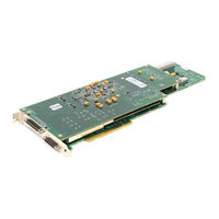
National Instruments DAQ PCI-4453 User Manual (122 pages)
Dynamic Signal Acquisition Device for PCI
Brand:
National Instruments
| Category:
PCI Card
| Size: 0 MB
Table of Contents
Table of Contents
4
About this Manual
9
How to Use the Manual Set
9
Conventions
9
Related Documentation
10
Chapter 1 Introduction
11
About the PCI-445X
11
What You Need to Get Started
12
Unpacking
13
Software Programming Choices
13
National Instruments Application Software
13
NI-DAQ Driver Software
14
Optional Equipment
15
Figure 1-1. the Relationship between the Programming Environment
15
Custom Cabling
16
Analog Cables
16
Analog Accessories
17
Digital Cables (PCI-4451/4452 Only)
17
Chapter 2 Installation and Configuration
18
Software Installation
18
Hardware Installation
18
Device Configuration
19
Chapter 3 Hardware Overview
20
Figure 3-1. Digital Function Block Diagram
20
Figure 3-2. PCI-4451/4452 Analog Function Block Diagram
21
Figure 3-3. PCI-4453/4454 Analog Function Block Diagram
22
Analog Input
23
Input Mode
23
Input Coupling
23
Input Polarity and Input Range
23
Considerations for Selecting Input Ranges
24
Table 3-1. Actual Input Range and Measurement Resolution
24
Analog Output (PCI-4451/4453 Only)
25
Output Mode
25
Output Polarity and Output Range
26
Table 3-2. Actual Output Range and Resolution of the PCI-4451
26
Trigger
27
Figure 3-4. Below-Low-Level Triggering Mode
28
Figure 3-5. Above-High-Level Triggering Mode
28
Figure 3-6. Inside-Region Triggering Mode
29
Figure 3-7. High-Hysteresis Triggering Mode
29
Figure 3-8. Low-Hysteresis Triggering Mode
29
RTSI Triggers
31
Digital I/O (PCI-4451/4452 Only)
31
Figure 3-9. RTSI Bus Signal Connection
31
Timing Signal Routing
32
Programmable Function Inputs (PCI-4451/4452 Only)
32
Device and RTSI Clocks
33
Selecting Sample/Update Clock Frequency
33
Device Configuration Issues
34
Chapter 4 Signal Connections
35
I/O Connectors
35
Analog I/O Connector Signal Descriptions
36
Figure 4-1. Analog Pin Connections for the PCI-4451/4452
36
Table 4-1. Analog I/O Connector Pin Assignment for the PCI-4451/4452
37
Table 4-2. Analog I/O Signal Summary for the PCI-4451/4452
38
Figure 4-2. Analog Pin Connections for the PCI-4453/4454
39
Table 4-3. Analog I/O Connector Pin Assignment for the PCI-4453/4454
40
Table 4-4. Analog I/O Signal Summary for the PCI-4453/4454
41
Digital I/O Connector Signal Descriptions
42
Figure 4-3. Digital Pin Connections
42
Table 4-5. Digital I/O Connector Pin Assignment
43
Table 4-6. Digital I/O Signal Summary
45
Analog Input Signal Connections
46
Figure 4-4. Analog Input Stage of the PCI-4451/4452
46
Figure 4-5. Analog Input Stage of the PCI-4453/4454
47
Types of Signal Sources
48
Floating Signal Sources
48
Ground-Referenced Signal Sources
48
Analog Output Signal Connections
48
Figure 4-6. Analog Output Channel Block Diagram for the PCI-4451
49
Analog Power Connections
50
Figure 4-7. Analog Output Channel Block Diagram for the PCI-4453
50
Digital I/O Signal Connections (PCI-4451/4452 Only)
51
Figure 4-8. Digital I/O Connections
51
Digital Power Connections (PCI-4451/4452 Only)
52
Timing Connections
52
Programmable Function Input Connections (PCI-4451/4452 Only)
53
Acquisition Timing Connections
53
Figure 4-9. Typical Posttriggered Acquisition
53
Figure 4-10. Typical Pretriggered Acquisition
54
PFI0/TRIG1 (EXT_TRIG) Signal
54
CONVERT* Signal
55
EXTSTROBE* Signal (PCI-4451/4452 Only)
55
PFI1/TRIG2 (PRETRIG) Signal
55
Waveform Generation Timing Connections
56
WFTRIG Signal
56
UPDATE* Signal
56
General-Purpose Timing Signal Connections
56
Figure 4-11. EXTSTROBE* Signal Timing
56
Figure 4-12. GPCTR0_SOURCE Signal Timing
57
GPCTR0_GATE Signal
57
GPCTR0_SOURCE Signal
57
Figure 4-13. GPCTR0_OUT Signal Timing
58
GPCTR0_UP_DOWN Signal (PCI-4451/4452 Only)
58
GPCTR1_SOURCE Signal (PCI-4451/4452 Only)
58
Figure 4-14. GPCTR1_SOURCE Signal Timing
59
GPCTR1_GATE Signal (PCI-4451/4452 Only)
59
Figure 4-15. GPCTR1_OUT Signal Timing
60
GPCTR1_OUT Signal (PCI-4451/4452 Only)
60
GPCTR1_UP_DOWN Signal (PCI-4451/4452 Only)
60
Figure 4-16. GPCTR Timing Summary
61
FREQ_OUT Signal (PCI-4451/4452 Only)
62
Field Wiring Considerations
62
Chapter 5 Calibration
64
Loading Calibration Constants
64
Self-Calibration
65
External Calibration
65
Traceable Recalibration
66
Chapter 6 Theory of Analog Operation
67
Functional Overview
67
Analog Input Circuitry
67
Input Coupling
69
Calibration
69
Antialias Filtering
69
Figure 6-1. Input Frequency Response
71
Figure 6-2. Input Frequency Response Near the Cutoff
72
Figure 6-3. Alias Rejection at the Oversample Rate for the PCI-4451/4452
73
Figure 6-4. Alias Rejection at the Oversample Rate for the PCI-4453/4454
74
The ADC
75
Figure 6-5. Comparison of a Clipped Signal to a Proper Signal
75
Noise
76
Analog Output Circuitry (PCI-4451/4453 Only)
77
Anti-Image Filtering
78
Figure 6-6. Signal Spectra in the DAC
79
The DAC
80
Calibration
80
Mute Feature
81
Appendix A Specifications
82
Figure A-1. PCI-4451/4452 Idle Channel Noise (Typical
86
Figure B-1. DB-25 Pinout for the SHC68-DB25 Cable
94
Appendix B Pin Connections
95
Figure B-2. 68-Pin Digital Connector for any Digital Accessory
95
Advertisement
Advertisement
Related Products
National Instruments DAQ PCI-4454
National Instruments PCI-485/2
National Instruments PCI-485/4
National Instruments PCIe-GPIB
National Instruments MXI PCIe-8374
National Instruments PCI-FBUS
National Instruments NI PCIe-1429
National Instruments PCI-232/8
National Instruments PCIe-8361
National Instruments PCI-7030/6030E
National Instruments Categories
Control Unit
I/O Systems
Controller
Computer Hardware
Measuring Instruments
More National Instruments Manuals
Login
Sign In
OR
Sign in with Facebook
Sign in with Google
Upload manual
Upload from disk
Upload from URL