Sign In
Upload
Manuals
Brands
MEN Mikro Elektronik Manuals
Motherboard
A14C - 6U VME64 MPC8540
MEN Mikro Elektronik A14C - 6U VME64 MPC8540 Manuals
Manuals and User Guides for MEN Mikro Elektronik A14C - 6U VME64 MPC8540. We have
1
MEN Mikro Elektronik A14C - 6U VME64 MPC8540 manual available for free PDF download: User Manual
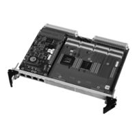
MEN Mikro Elektronik A14C - 6U VME64 MPC8540 User Manual (121 pages)
Brand:
MEN Mikro Elektronik
| Category:
Motherboard
| Size: 1 MB
Table of Contents
Technical Data
3
Block Diagram
7
Configuration Options
8
About this Document
11
Legal Information
12
Table of Contents
13
1 Getting Started
19
Maps of the Board
19
Figure 1. Map of the Board - Front View
19
Figure 2. Map of the Board - Top View
20
Configuring the Hardware
21
Integrating the Board into a System
22
Installing Operating System Software
23
2 Functional Description
24
Power Supply
24
Watchdog
24
Clock Supply
24
Real-Time Clock
24
Powerpc CPU
25
General
25
Thermal Considerations
25
Bus Structure
26
Host-To-PCI Bridge
26
Local PCI Bus
26
PCI-To-PCI Bridge
26
PCI-To-Vmebus Bridge
26
Memory
27
DRAM System Memory
27
Boot Flash
27
NAND Flash
27
Fram
27
Additional SDRAM
27
Eeprom
27
IDE Interface
28
Connection
28
Table 1. Pin Assignment of 44-Pin IDE Plug Connector
28
Figure 3. Position of Fuse for IDE Protection
29
Table 2. Signal Mnemonics of 44-Pin IDE Plug Connector
29
Installing a Hard Disk
30
Ethernet Interfaces
32
Connection
32
Table 3. Signal Mnemonics of Ethernet 10Base-T/100Base-Tx/1000Base-TX
32
Interfaces
32
Table 4. Pin Assignment of 8-Pin RJ45 Ethernet 10Base-T/100Base-Tx/1000Base-TX Connectors (LAN1
32
Table 5. Pin Assignment of 9-Pin D-Sub 10Base-T/100Base-TX Plug Connector
33
(LAN1 and LAN2)
33
Table 6. Pin Assignment of 9-Pin D-Sub 10Base-T/100Base-TX Plug Connector
33
(LAN3 and COM1)
33
General
34
10Base-T
34
UART COM1 Interface
35
Table 7. Signal Mnemonics of UART COM1 Interface
35
Table 8. Pin Assignment of 8-Pin RJ45 UART Connector (COM1)
35
Table 9. Pin Assignment of 9-Pin D-Sub COM1/LAN3 Plug Connector
36
UART COM10 Interface
37
UART COM20..COM23 Interfaces
38
Table 10. Signal Mnemonics for UART COM20
38
Connection Via 40-Pin Connector
39
Table 11. Pin Assignment of the 40-Pin UART COM20..COM23 Connector
39
Connection Via 10-Pin SA-Adapter Connectors
42
Table 12. Pin Assignment of the 10-Pin UART COM20..COM23 Connectors
42
Figure 4. Installing SA-Adapters on A14C Directly
43
Figure 5. Position of Fuse for COM20..COM23 Protection
44
Gpio
45
Table 13. Assignment of 16Z034_GPIO Controllers
45
PMC Slots
46
Installing a PMC Mezzanine Module
47
Figure 6. Installing a PMC Mezzanine Module
47
Board-To-Board I/O Connector
48
Table 14. Pin Assignment of I/O Connector J2 - Factory Standard FPGA
49
Configuration
49
Table 15. Signal Mnemonics of I/O Connector J2 - Factory Standard FPGA
50
Reset Button
51
Figure 7. Position of Reset Button
51
Vmebus Interface
52
PCI Configuration Space Registers
53
Configuration
53
Table 16. Vmebus Interface PCI Configuration Space Registers
53
Runtime Registers
54
Table 17. Vmebus Runtime Registers
54
Table 18. Vmebus Interface BAR 0
55
Table 19. Vmebus Interface BAR1
55
Table 20. Vmebus Interface BAR2
55
Table 21. Vmebus Interface BAR3
55
Table 22. Vmebus Interface BAR4
55
Vmebus Master Mapping
55
Sram
56
Table 23. Vmebus Slave Address Windows
56
VME Slave Mapping
56
Slot-1 Function
57
Vmebus Master Interface
58
Table 24. Vmebus Interface Valid Combinations for Byte Enables Supported by PCI
59
To-VME Bridge
59
Table 25. Vmebus Master Address Modifier Codes
61
Vmebus Slave Interface
62
Table 26. Vmebus Slave Address Modifier Codes
66
Vmebus Requester
67
Vmebus Interrupt Handler
68
Vmebus Interrupter
69
A32 Address Mode
70
Mailbox
71
Location Monitor
72
DMA Controller
74
Connection
76
Table 27. Pin Assignment of VME64 Connector P1
76
Table 28. Pin Assignment of Vmebus Rear I/O Connector P2 - PMC Signals
78
Table 29. Signal Mnemonics of Vmebus Rear I/O Connector P2 - PMC 0
79
Table 31. Signal Mnemonics of Vmebus Rear I/O Connector P2 - FPGA I/O
81
3 Fpga
82
General
82
Figure 8. FPGA - Block Diagram
82
System Unit
83
Functional Description
83
Address Organization
85
Table 32. FPGA - Address Map
85
Standard Factory FPGA Configuration
92
IP Cores
92
FPGA Configuration Table
92
Table 33. FPGA - Factory Standard Configuration Table for A14C
92
4 Menmon
93
General
93
State Diagram
94
Figure 9. MENMON - State Diagram, Degraded Mode/Full Mode
94
Figure 10. MENMON - State Diagram, Main State
95
Interacting with MENMON
96
Entering the Setup Menu/Command Line
96
Configuring MENMON for Automatic Boot
96
Updating Boot Flash and NAND Flash
97
Update Via the Serial Console Using SERDL
97
Update from Network Using NDL
97
Update Via Program Update Menu
97
Table 34. MENMON - Program Update Files and Locations
97
Automatic Update Check
98
Diagnostic Tests
99
Ethernet
99
Table 35. MENMON - Diagnostic Tests: Ethernet
99
SDRAM and FRAM
100
Table 36. MENMON - Diagnostic Tests: SDRAM and FRAM
100
Eeprom
101
Table 37. MENMON - Diagnostic Tests: EEPROM
101
IDE/NAND Flash
102
COM1 Port
102
Table 38. MENMON - Diagnostic Tests: IDE/NAND Flash
102
Table 39. MENMON - Diagnostic Tests: COM1 Port
102
Primary/Secondary MENMON
103
Hardware Monitor Test
103
Rtc
103
Table 40. MENMON - Diagnostic Tests: Primary/Secondary MENMON
103
Table 41. MENMON - Diagnostic Tests: Hardware Monitor
103
Table 42. MENMON - Diagnostic Tests: RTC
103
MENMON Configuration and Organization
104
Consoles
104
Video Modes
104
Abort Pin
104
Table 43. MENMON - System Parameters for Console Selection
104
MENMON Memory Map
105
Table 44. MENMON - Address Map (Full-Featured Mode)
105
Table 45. MENMON - Boot Flash Memory Map
105
MENMON BIOS Logical Units
106
Table 46. MENMON - Controller Logical Units (Cluns)
106
Table 47. MENMON - Device Logical Units (Dluns)
106
System Parameters
107
Table 48. MENMON - A14C System Parameters - Autodetected Parameters
107
Table 49. MENMON - A14C System Parameters - Production Data
108
Table 50. MENMON - A14C System Parameters - MENMON Persistent
109
Parameters
109
Table 51. MENMON - A14C System Parameters - Vxworks Bootline
111
Parameters
111
Table 52. MENMON - Reset Causes through System Parameter Rststat
112
Table 53. MENMON - Voltage Limits through System Parameter Psrxxx
112
MENMON Commands
113
Table 54. MENMON - Command Reference
113
5 Organization of the Board
115
Memory Mappings
115
Table 55. Memory Map - Processor View
115
Table 56. Address Mapping for PCI
115
Interrupt Handling
116
SMB Devices
116
Table 57. Dedicated Interrupt Line Assignment
116
Table 58. Interrupt Numbering Assigned by MENMON
116
Table 59. SMB Devices
116
PCI Devices on Bus 0
117
Table 60. PCI Devices on Bus 0
117
6 Appendix
118
Literature and Web Resources
118
Powerpc
118
Ide
118
Ethernet
118
Pmc
119
119
119
Vmebus
119
Finding out the Board's Article Number, Revision and Serial
119
Number
119
Figure 11. Label Giving the Board's Article Number, Revision and Serial Number
119
Advertisement
Advertisement
Related Products
MEN Mikro Elektronik G20-3U
MEN Mikro Elektronik G22
MEN Mikro Elektronik Categories
Network Router
Motherboard
Desktop
Switch
Control Unit
More MEN Mikro Elektronik Manuals
Login
Sign In
OR
Sign in with Facebook
Sign in with Google
Upload manual
Upload from disk
Upload from URL