Sign In
Upload
Manuals
Brands
MEN Mikro Elektronik Manuals
Desktop
A11
MEN Mikro Elektronik A11 Manuals
Manuals and User Guides for MEN Mikro Elektronik A11. We have
1
MEN Mikro Elektronik A11 manual available for free PDF download: User Manual
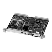
MEN Mikro Elektronik A11 User Manual (108 pages)
6U VMEbus PowerPC Workstation
Brand:
MEN Mikro Elektronik
| Category:
Desktop
| Size: 1 MB
Table of Contents
Technical Data
3
About this Document
8
Table of Contents
10
1 Getting Started
16
Map of the Board
16
Figure 1. Map of the Board - Front Panel and Top View
16
Configuring the Hardware
17
Integrating the Board into a System
18
Table 1. Terminal Lines of the 9-Pin Micro D-Sub RS232 Plug Connector
18
Installing Operating System Software
19
2 Functional Description
20
Power Supply
20
Clock Supply
20
Powerpc CPU
21
General
21
Heat Sink
21
Table 2. Powerpc Compare Chart
21
Bus Structure
22
Host-To-PCI Bridge
22
Local PCI Bus
22
PCI-To-ISA Bridge
22
PCI-To-PCI Bridge
22
PCI-To-Vmebus Bridge
22
Memory
23
Level 2 Cache
23
Sdram
23
Figure 2. SO-DIMM DRAM Installation
23
Flash
24
Eeprom
24
Figure 3. Position of Flash on Bottom Side of A11
24
Ethernet Interface
25
Connection
25
Table 3. Pin Assignment of the 8-Pin RJ45 Ethernet 10Base-T/100Base-T
25
Table 4. Signal Mnemonics of the Ethernet 10Base-T/100Base-T Connector
25
General
26
10Base-5
26
10Base-T
26
100Base-T
27
SCSI Interface
28
Connection
28
Table 5. Signal Mnemonics for SCSI Interface
28
Table 6. Pin Assignment of the 68-Pin VHDCI SCSI Connector
29
General
30
Table 7. Overview of SCSI Types, Maximum Bus Widths, Throughput and Line
31
Lengths
31
SCSI Termination on A11
32
Figure 4. SCSI Termination on A11
32
Table 8. SCSI Termination on A11
32
PCI Expansion
33
Table 9. Pin Assignment of the 114-Pin PCI Expansion Connector
34
PC•MIP Slots
35
Installing Pc•Mips
35
Figure 5. Installation of a PC•MIP
35
PC•MIP Connectors
36
Compactflash
37
Installing Compactflash
37
Supported Compactflash Cards
37
Figure 6. Compactflash Card
37
Keyboard/Mouse
38
Table 10. Pin Assignment of the 6-Pin Mini DIN Keyboard/Mouse Connector
38
Table 11. Signal Mnemonics for Keyboard/Mouse Interface
38
Serial Ports COM1/COM2
39
Connection
39
Table 12. Pin Assignment of the 9-Pin Micro D-Sub COM1/COM2 Plug Connectors
39
Table 13. Signal Mnemonics for RS232 Serial Ports COM1/COM2
39
Asynchronous/Synchronous Serial Ports COM3/COM4
40
Figure 7. COM4 Clock Signals - Principle
40
Table 14. Configuring Clock Signals for COM4
40
Enhanced Parallel Port
41
Figure 8. Jumpers for Clock Selection for COM4
41
Floppy Disk Controller
42
Table 15. Pin Assignment of 26-Pin ZIF Floppy Disk Drive Connector
42
Table 16. Signal Mnemonics for Floppy Disk Drive Connector
43
Hardware Monitor
44
Timekeeper, NVRAM and Watchdog
44
Counter/Timer CIO Z8536
44
Table 17. Hardware Monitor Channels
44
Reset/Abort Buttons and User/Status Leds
45
Reset/Abort Buttons
45
User/Status Leds
45
Figure 9. Reset/Abort Buttons and User Leds
45
Table 18. User/Status LED Functions
45
User-Defined Hex Switch
46
Figure 10. Position of Hex Switch
46
Vmebus Interface
47
Implementation on the Board
47
Figure 11. Vmebus Interrupts
48
Connection
49
Connector
49
Table 19. Pin Assignment of the 5/3-Row, 96/160-Pin Vmebus Connector P1
50
Table 20. Pin Assignment of the 5/3-Row, 96/160-Pin Vmebus Connector P2
51
Table 21. Signal Mnemonics of Vmebus Rear I/O Connector P2
52
Figure 12. Connection of a Rear I/O Adapter (E.g. Men's AD39)
54
IEEE 1149.1 (JTAG)/COP Test Interface
55
Table 22. Pin Assignment of the 16-Pin IEEE 1149.1 Test Connector
55
Configuring the COP Test Interface
56
Configuring the IEEE 1149.1 Test Interface
56
Figure 13. Connector and Jumper for IEEE 1149.1 Test Interface
56
Figure 14. Resistors for COP Test Interface
56
3 Menmon
57
General
57
Console
57
A11 MENMON Memory Map
58
Figure 15. MENMON - Address Mapping
58
MENMON Start-Up
59
User Leds
59
Boot Sequence
59
Configuring the MENMON Start-Up Procedure
59
Self Tests
60
Figure 16. MENMON - Power on Self Test Output with Self Test Message Mode
60
Extended
60
MENMON Boot Methods for Client Programs
62
MENMON BIOS Devices
62
Table 23. MENMON - Assignment for A11 Controller Devices
63
Disk Boot
64
Figure 17. MENMON - Layout of the 0X41-Type Partition (Prep)
64
Figure 18. MENMON - Single Boot-Image CD-ROM Configuration
65
Network Boot
70
MENMON Tape Boot
71
Updating Flash Devices
72
Download Via Serial Interface
72
Table 24. MENMON - Download Destination Devices
72
Performing the Download
73
Table 25. MENMON - Flash Sectors for 8MB
73
Table 26. MENMON - Flash Sectors for 16MB
73
Update from Disk or Network
74
MENMON User Interface
75
Command Line Editing
75
Numerical Arguments
75
MENMON Command Overview
76
Table 27. MENMON - Command Overview
76
Board Setup
78
Ali 1543
78
PCI Auto-Configuration
78
Vmebus
80
Table 28. MENMON - Address Map for A11 as a Vmebus Master
80
Scsi
81
SDRAM DIMM Configuration
81
Hex Switch
81
Table 29. MENMON - Hex-Switch Settings
81
MENMON System Calls
82
Invoking System Calls
82
System Calls
83
Table 30. MENMON - System Calls - BRD_ID Fields
83
Table 31. MENMON - System Calls - RTC_RD Buffer Data
85
Table 32. MENMON - System Calls - DSK_RD Fields
86
Vxworks Bootline
88
Table 33. MENMON - Vxworks Bootline - List of Parameters and Their
88
Additional MENMON Parameters
89
Table 34. MENMON - Common Parameters Passed by All Menmons
89
4 Organization of the Board
90
Memory Mappings
90
Processor View of the Memory Map
90
Table 35. Address Map - Processor View
90
PCI Configuration Space Map (Primary Bus)
91
PCI Configuration Space Map (Secondary Bus)
91
Table 36. PCI Configuration Space Map (Primary Bus)
91
Table 37. PCI Configuration Space Map (Secondary Bus)
91
PCI/ISA I/O Space Memory Map
92
Table 38. PCI/ISA I/O Space Memory Map
92
Vmebus Memory Map
93
Table 39. Possible Vmebus Memory Map
93
Interrupt Handling
94
Figure 19. A11 Interrupt Structure
94
Maskable Interrupts
95
Nonmaskable Interrupts
95
Table 40. ISA Interrupt Assignments
95
Table 41. Steerable Interrupt Assignments
95
Table 42. PCI Interrupt Assignments
95
Implementation of SYM53C895 SCSI Controller
96
Table 43. General-Purpose Pins of SYM53C895 SCSI Controller
96
Implementation of M1543 PCI-To-ISA Bridge
97
Table 44. M1543 General Purpose Input (GPI) Pin Assignments
97
Table 45. M1543 General Purpose Input/Output (GPIO) Pin Assignments
97
Table 46. M1543 General Purpose Output Pin Assignments
98
Table 47. M1543 GPI Assignment for Hex Switch
98
Z8536 Cio
99
Table 48. Pin Assignment of the Z8536 Ports
99
5 Appendix
100
Literature and WWW Resources
100
Bridges
100
Vmebus
100
Pci
100
Ethernet
101
Scsi
101
Parallel Port
101
Pc•Mip
102
Miscellaneous
102
Board Revisions
102
Table 49. Table of Hardware Revisions
102
Component Plans
105
Figure 20. Component Plan of A11 Hardware Revision 03 - Top Side
105
Figure 21. Component Plan of A11 Hardware Revision 03 - Bottom Side
106
Advertisement
Advertisement
Related Products
MEN Mikro Elektronik BL50S
MEN Mikro Elektronik Categories
Motherboard
Network Router
Control Unit
Desktop
Switch
More MEN Mikro Elektronik Manuals
Login
Sign In
OR
Sign in with Facebook
Sign in with Google
Upload manual
Upload from disk
Upload from URL