Sign In
Upload
Manuals
Brands
M13design Manuals
Motherboard
M13- RA6M3-EK-SDRAM
M13design M13- RA6M3-EK-SDRAM Manuals
Manuals and User Guides for M13design M13- RA6M3-EK-SDRAM. We have
1
M13design M13- RA6M3-EK-SDRAM manual available for free PDF download: User Manual
M13design M13- RA6M3-EK-SDRAM User Manual (52 pages)
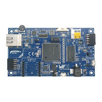
RA6M3 (Cortex-M4) Evaluation Kit
Brand:
M13design
| Category:
Motherboard
| Size: 3 MB
Table of Contents
Table of Contents
2
Overview
7
Introduction
7
Figure 1. M13-RA6M3-EK Component View (Top)
7
Figure 2. M13-RA6M3-EK LCD View (Bottom)
7
Features
8
Hardware Layout and Configuration
9
Hardware Block Diagram
9
Figure 3. Bloc Diagram
9
The M13-RA6M3-EK Board Layout
10
Figure 4. Top Main Component Layout
10
Figure 5. Bottom Main Component Layout (Bottom View)
10
Table 1. Top Main Component List
11
Table 2. Bottom Main Component List
11
M13-Ra6M3-Ek Pin Assignment
12
RA6M3 System and Power Pins
12
Boot Pin
12
System Reset Pin
12
Table 3. Boot Pins
12
Table 4. JP2
12
Table 5. System Reset Pin
12
Figure 6. Reset Block Diagram
12
Clock Source
13
Table 6. Clock Source Assignment
13
Figure 7. Clock Source Diagram
13
Power Supply
14
Figure 8. RA6M3 Power Supply Overview
14
External Memory
15
Serial Flash Memory
15
Table 7. Serial Flash Memory Overview
15
Table 8. Serial Flash Memory Pin Assignment
15
Sdram
16
Table 9. SDRAM Overview
16
Table 10. SDRAM Address Bus Pin Assignment
16
Eeprom
17
Table 11. EEPROM Overview
17
Table 12. IIC0 Pin Assignment
17
4.3-Inch Tft Lcd Module
18
Table 13. TFT LCD Module Overview
18
Table 14. Capacitive Touchscreen
18
Table 15. LCD Assignment Pins
18
USB Interface
19
Table 16. USB Overview
19
Table 17. USB Pin Assignment
19
Figure 9. USB Diagram
19
LAN Interface
20
Table 18. Ethernet PHY Overview
20
Table 19. Ethernet Assignment Pins
20
Table 20. P706 Multiplexing
20
SD/MMC Host Interface (4-Bits)
21
Table 21. SD/MMC Interface Pin Assignment
21
Figure 10.SD/MMC Host Interface Diagram
21
Audio Interface
22
Table 22. Audio CODEC Overview
22
Table 23. Audio Pin Assignment
22
Figure 11. Audio Block Diagram
22
3-Axis Accelerometer
23
Table 24. Accelerometer Overview
23
Table 25. IIC0 Pin Assignment
23
J-Link ob
24
Table 26. SWD/JTAG Pin Assignment
24
Figure 12. Debug Interface Diagram
24
Table 27. Debug Configuration
25
Figure 13. SW2 Illustration
25
VGA Camera Module
26
Table 28. VGA Camera Module Overview
26
Table 29. 8Bit VGA Interface Pin Assignment
26
I²C Interface
27
Table 30. I²C Pin Assignment
27
Figure 14. I²C Bus Diagram
27
User Interface: Switch, Led, Potentiometer
28
Table 31. User Interface Overview
28
Table 32. User Interface Pin Assignment
28
Figure 15. User Interface Diagram
28
Connector Overview
29
CN1: USB-Micro A/B
29
CN2: USB-Micro A/B
29
Table 33. CN1 Pin Description
29
Table 34. CN2 Pin Description
29
Figure 16. CN1: USB-Micro A/B Front View
29
Figure 17. CN2: USB- Micro A/B Front View
29
CN4: 19-Pin JTAG Header
30
Table 35. CN4 Pin Assignment
30
Figure 18. CN4: 19-Pin JTAG Header
30
Cn6: Rj45
31
Table 36. CN6 Pin Assignment
31
Figure 19. CN6. RJ45 Bottom View
31
CN7: LCD Connector
32
Table 37. CN7 Pin Assignment
32
Figure 20. CN7. Front View
32
CN8: LCD Capacitive Touch
33
CN9: 8 Bit VGA Camera Module
33
Table 38. CN8 Pin Assignment
33
Table 39. CN9 Pin Assignment
33
Figure 21. CN8 Front View
33
Figure 22. CN9 Front View
33
CN10: Micro SD Card
34
Table 40. CN10: Micro SD Card Pin Assignment
34
Figure 23. CN10: Microsd Card Bottom View
34
CN11: 4-Pole Audio Jack
35
Table 41. CN11 Pin Assignment
35
Figure 24. CN11 Mating Plug and Bottom View
35
CN12: Expansion Connector - Mikrobus
36
Table 42. CN12 Pin Assignment
36
Table 43. Mikrobus
36
Figure 25. CN12 Mikrobus
36
CN13/CN14: Expansion Connectors - PMOD
37
Table 44. PMOD Connector Overview
37
Table 45. CN13 (PMOD1) Pin Assignment
37
Figure 26. PMOD Front View
37
Table 46. CN14 (PMOD2) Pin Assignment
38
CN15: +5VDC Power Jack
39
Table 47. CN15 Connector Overview
39
Table 48. CN15 Pin Assignment
39
Figure 27. CN15 Power Jack
39
Multiplexed Functions
40
Table 49. Multiplexing Function Table
40
Figure 28. Shunt Footprint
40
SDRAM Selection
41
Figure 29. Shunt General Location
41
Data / Spi0
42
Addr / Ssie0
42
Addr / Sci2
42
Table 50. Multiplexing SDRAM Data & SPI0
42
Table 51. Multiplexing SDRAM Addresses & SSIE0
42
Table 52. Multiplexing SDRAM Addresses & SCI2
42
Addr / Sci6
43
Pmod2
43
Table 53. Multiplexing SC6 & SDRAM Addresses
43
Table 54. Multiplexing PMOD_RST & SDRAM Address
43
Default" and "SDRAM Ready" Shunt Configuration Recap
44
Table 55. Shunt Configuration
44
Sd Card / Qspi
45
Table 56. QSPI/SDHI Selection
45
Figure 30. JP3 to JP8 Top Location
45
Tdi / Cts2 / Irq11
46
Table 57. Multiplexing TDI / CTS2 / IRQ11
46
Sda0_B / Usb_Vbus
47
Table 58. Multiplexing SDA0_B & USB_VBUS
47
Related Documents
48
Ordering Information
49
Table 59. Ordering Information
49
Table 60. Default/Sdram-Ready Features
49
Technology Partners
50
Table 61. Hardware Technology Partners
50
Table 62. Software Technology Partners
50
Revision History
51
Table 63. Revision Table
51
Advertisement
Advertisement
Related Products
M13design M13-RA6M3-EK
M13design M13- RA6M3-EK-VGA
M13design M13- RA6M3-EK-WIFI
M13design Categories
Motherboard
More M13design Manuals
Login
Sign In
OR
Sign in with Facebook
Sign in with Google
Upload manual
Upload from disk
Upload from URL