
Summary of Contents for M13design M13-RA6M3-EK
- Page 1 M13-RA6M3-EK RA6M3 (Cortex-M4) Evaluation Kit USER MANUAL M13-RA6M3-EK Board name: MCU: R7FA6M3AH3CFC Updated on the: 16 Dec. 21 Version 1.0.3...
-
Page 2: Table Of Contents
Introduction ..........................7 Features ........................... 8 HARDWARE LAYOUT AND CONFIGURATION ................9 Hardware block diagram ......................9 The M13-RA6M3-EK Board layout ..................10 M13-RA6M3-EK PIN ASSIGNMENT ..................... 12 RA6M3 system and Power pins ..................... 12 3.1.1 Boot pin ........................12 3.1.2... - Page 3 “Default” and “SDRAM ready” shunt Configuration recap ........... 44 SD CARD / QSPI ........................45 TDI / CTS2 / IRQ11 ........................ 46 SDA0_B / USB_VBUS ......................47 RELATED DOCUMENTS ......................48 ORDERING INFORMATION......................49 TECHNOLOGY PARTNERS ......................50 REVISION HISTORY ........................51 M13design - 16 Dec. 21 3/53...
- Page 4 Table 35. CN4 Pin Assignment ......................30 Table 36. CN6 Pin Assignment ......................31 Table 37. CN7 Pin Assignment ......................32 Table 38. CN8 Pin Assignment ......................33 Table 39. CN9 Pin Assignment ......................33 M13design - 16 Dec. 21 4/53...
- Page 5 Table 58. Multiplexing SDA0_B & USB_VBUS ..................47 Table 59. Ordering Information ......................49 Table 60. Default/SDRAM-Ready Features ..................49 Table 61. Hardware Technology Partners ..................... 50 Table 62. Software Technology Partners ....................50 Table 63. Revision Table ........................51 M13design - 16 Dec. 21 5/53...
- Page 6 LIST OF FIGURES Figure 1. M13-RA6M3-EK Component View (Top) ................. 7 Figure 2. M13-RA6M3-EK LCD View (Bottom) ..................7 Figure 3. Bloc Diagram ..........................9 Figure 4. Top main component Layout ....................10 Figure 5. Bottom main component layout (Bottom view) ..............10 Figure 6.
-
Page 7: Overview
M13-RA6M3-EK_UM - Rev1.0.2 Overview OVERVIEW INTRODUCTION The M13-RA6M3-EK is complete evaluation and development platform for the Renesas Electronics ® 32-bit Microcontroller RA family Cortex ® -M4 based R7FA6M3AH3CFC microcontroller. The full range of the hardware features on the board helps users to quickly evaluate all the available peripherals (10/100-... -
Page 8: Features
1 x 2.1mm 5V Power Jack • 2 x User switch and 1 x Reset switch 1 x Mono-turn 10KΩ Potentiometer • 3 x User LEDs • 1 x Power-on LED • M13design - 16 Dec. 21 8/53... -
Page 9: Hardware Layout And Configuration
MODE SEL. USER RST from P201 GPIOS SW/LED JLINK-OB Audio 4-Pole DC/DC 1V8 SSIF-2 / RIIC Codec 3.5mm Jack 2.1mm SPI/UART DC/DC 3V3 MIKROBUS JACK IRQ/GPIOs PMOD X 2 IRQ/GPIOs Figure 3. Bloc Diagram M13design - 16 Dec. 21 9/53... -
Page 10: The M13-Ra6M3-Ek Board Layout
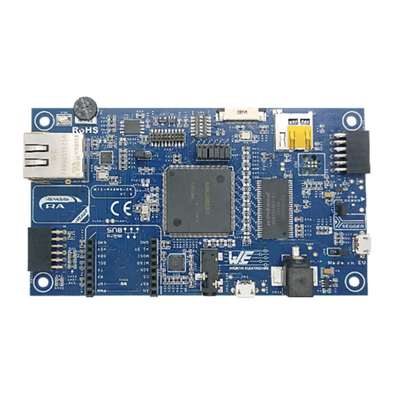
M13-RA6M3-EK_UM - Rev1.0.2 Hardware layout and configuration THE M13-RA6M3-EK BOARD LAYOUT Figure 4 and Figure 5 Show the layout of the main components of the board. Figure 4. Top main component Layout U8: SERIAL FLASH CN4: JTAG 19PINS CN9: CAMERA... -
Page 11: Table 1. Top Main Component List
M13-RA6M3-EK_UM - Rev1.0.2 Hardware layout and configuration Table 1 Table 2 list the main component mounted on the M13-RA6M3-EK board Table 1. Top main component list Component Description / MPN NOTES Reference Renesas / R7FA6M3AH3CFC Ethernet PHY Microchip / KSZ8081RNA... -
Page 12: M13-Ra6M3-Ek Pin Assignment
Function RESET# Reset nRESET_SYS System The M13-RA6M3-EK System Reset signal is controlled by 3 sources: The power-on reset with the Voltage supervisor U4, the Reset Switch (SW1) and the JTAG reset signal. Figure 6 shows the reset block diagram. Figure 6. Reset Block Diagram... -
Page 13: Clock Source
User Manual - Rev1.0.2 M13-RA6M3-EK pin assignment 3.1.3 CLOCK SOURCE The M13-RA6M3-EK has 2 clock input sources as shown in Figure 7 Table 6 gives you the connections for each clock on the RA6M3. - Main clock : 24MHz crystal - RTC clock : 32.768KHz crystal... -
Page 14: Power Supply
M13-RA6M3-EK pin assignment 3.1.4 POWER SUPPLY The M13-RA6M3-EK has 2 sources for its power supply. The Primary source is from the +5VDC/500mA of the J-Link OB USB connector CN5 as shown in Figure 8. The Secondary source is provided through the 2.10mm Power Jack connector CN15 and is strictly limited to a +5VDC power supply. -
Page 15: External Memory
3.2.1 SERIAL FLASH MEMORY The M13-RA6M3-EK board is equipped with a serial flash memory which is controlled by RA6M3 on- chip Quad Serial Peripheral Interface (QSPI). By default, the Serial Flash Memory is connected to the MCU but it can be switched to SD Card anytime. -
Page 16: Sdram
User Manual - Rev1.0.2 M13-RA6M3-EK pin assignment 3.2.2 SDRAM The M13-RA6M3-EK is also equipped with an external 16 bits SDRAM. This memory device is controlled by the RA6M3 Bus State Controller. Table 9 shows the SDRAM Memory Overview while Table 10 shows the pin assignment between the RA6M3 and the SDRAM device. -
Page 17: Eeprom
User Manual - Rev1.0.2 M13-RA6M3-EK pin assignment 3.2.3 EEPROM An EEPROM is also available on the M13-RA6M3-EK board. This memory device is controlled by the RA6M3 I²C Interface on channel 0 (IIC0) which is the board’s main I²C bus. Table 11 shows the EEPROM Memory Overview. -
Page 18: 4.3-Inch Tft Lcd Module
Note 3: Connected to the LCD Display signal and configured as a general GPIO in output mode with an On/Off behaviour. Note 4: Data Enable The LCD signal inputs are assigned in RGB888 format and connected onto the RA6M3 in BGR, little Indian arrangement. M13design - 16 Dec. 21 18/53... -
Page 19: Usb Interface
Note 3: Surface Mount Device Note 4: As the VBUSEN pin for the USBFS module is not available due to being used by other peripherals, P014 is configurated as a GPIO to ensure the said function. M13design - 16 Dec. 21 19/53... -
Page 20: Lan Interface
User Manual - Rev1.0.2 M13-RA6M3-EK pin assignment LAN INTERFACE The M13-RA6M3-EK embarks an Ethernet PHY (U7) which communicate through the RA6M3 on-chip ethernet controller ETHERC by using the RMII Interface. The details of this device can be seen in Table 18. -
Page 21: Sd/Mmc Host Interface (4-Bits)
User Manual - Rev1.0.2 M13-RA6M3-EK pin assignment SD/MMC HOST INTERFACE (4-BITS) The M13-RA6M3-EK board embarks a microSD card connector which is connected to the RA6M3’s SD/MMC Host Interface on channel 1 as shown in Figure 10 Table 21 and uses a 4-bit wide interface. -
Page 22: Audio Interface
M13-RA6M3-EK pin assignment AUDIO INTERFACE The M13-RA6M3-EK is equipped with a Maxim Audio CODEC (U13) for audio features. It’s configurations and controls are done through the I²C interface using channel 0. While the exchange of audio data is done using the Serial Sound Interface (SSIE) channel 0. -
Page 23: 3-Axis Accelerometer
User Manual - Rev1.0.2 M13-RA6M3-EK pin assignment 3-AXIS ACCELEROMETER The M13-RA6M3-EK board is equipped with a 3-Axis Accelerometer from Wurth Electronics. This device is controlled by the RA6M3 I²C Interface on channel 0 (IIC0) as shown in Table Table 24 shows the device overview. -
Page 24: J-Link Ob
M13-RA6M3-EK pin assignment J-LINK OB The M13-RA6M3-EK board embarks a J-Link OB from Segger, which is the board’s default debugging and programming probe. The J-Link OB supports JTAG, SWD (+SWO) and one VCOM interface. Through its USB connector (CN5) the J-Link OB is also the board main 5VDC power supply. -
Page 25: Table 27. Debug Configuration
In order to use the J-Link OB, make sure to slide all the SW2 switches on the “On” position. See Figure 13, which represents the PCB Top side, to have a better visualization of the “On/Off” positioning of SW2. Figure 13. SW2 Illustration SW2 ‘ON’ POSITION SW2 ‘OFF’ POSITION M13design - 16 Dec. 21 25/53... -
Page 26: Vga Camera Module
3.10 VGA CAMERA MODULE The M13-RA6M3-EK board is also capable to drive VGA camera modules with its Parallel Data Capture Unit (PDC). Through the connector CN8, we provide an 8-bit interface which is compatible with many modules actually on the market. -
Page 27: I²C Interface
User Manual - Rev1.0.2 M13-RA6M3-EK pin assignment 3.11 I²C INTERFACE The M13-RA6M3-EK board uses two I²C channels which are divided between the I²C Bus Interface module (IIC) and the Serial Communication Interface (SCI). Table 30 shows you how each of these channels are mapped on the board. -
Page 28: User Interface: Switch, Led, Potentiometer
Green AN007 / P003 3352T-1-103LF P006 PTS645SM43SMTR92LFS The M13-RA6M3-EK board contains 2 User Switches and 3 User Leds (Green coloured) as described Table 32 and is also equipped with a 10K mono-turn Potentiometer. Table 31. User Interface Overview Device Type... -
Page 29: Connector Overview
Note VBUS CN1_VBUS USBFS_DM USBFS_DP CN2: USB-MICRO A/B Figure 17. CN2: USB- Micro A/B Front view Table 34. CN2 Pin Description CN2 Pin Pin Description Signal Name RA6M3 Pin Note VBUS CN2_VBUS USBHS_DM USBHS_DP M13design - 16 Dec. 21 29/53... -
Page 30: Cn4: 19-Pin Jtag Header
Not used Multiplexed nRESET nRESET Not used P214 / TCLK TCLK Multiplexed Not used P211 / TDATA0 TDATA0 Multiplexed P210 / TDATA1 TDATA1 Multiplexed P209 / TDATA2 TDATA2 Multiplexed P208 / TDATA3 TDATA3 Multiplexed M13design - 16 Dec. 21 30/53... -
Page 31: Cn6: Rj45
User Manual - Rev1.0.2 Connector Overview CN6: RJ45 Figure 19. CN6. RJ45 Bottom View Table 36. CN6 Pin Assignment CN6 Pin Pin Description Signal Name U7 Pin Note LED1+ 3V3D LED1- LED2+ 3V3D LED2- ET0_LED2 P806 M13design - 16 Dec. 21 31/53... -
Page 32: Cn7: Lcd Connector
LCD_DATA06_B LCD_DATA07_B LCD_DATA08_B LCD_DATA09_B LCD_DATA10_B LCD_DATA11_B LCD_DATA12_B LCD_DATA13_B LCD_DATA14_B LCD_DATA15_B LCD_DATA16_B LCD_DATA17_B LCD_DATA18_B LCD_DATA19_B LCD_DATA20_B LCD_DATA21_B LCD_DATA22_B LCD_DATA23_B PLCK LCD_CLK_B DISP LCD_DISP I/O Port HSYNC LCD_TCON1_B VSYNC LCD_TCON2_B LCD_TCON3_B None None None None None M13design - 16 Dec. 21 32/53... -
Page 33: Cn8: Lcd Capacitive Touch
VSYNC VSYNC PWDN CAM_PWR_DN HSYNC HSYNC HREF VCORE None 100nF to GND DVDD 3V3D PIXD7 XCLK XLCK multiplexed PIXD6 DGND PIXD5 PCLK PIXCLK PIXD4 PIXD0 PIXD3 PIXD1 PIXD2 None Not used None Not used M13design - 16 Dec. 21 33/53... -
Page 34: Cn10: Micro Sd Card
Pin Description Signal Name RA6M3 Pin Note DAT2 SD1DAT2_A Multiplexed DAT3/CD SD1DAT3_A Multiplexed SD1CMD_A Multiplexed 3V3D SD1CLK_A Multiplexed DAT0 SD1DAT0_A Multiplexed DAT1 SD1DAT1_A Multiplexed 9 & 11 CARD DETECT None 10 & 12 COMMON M13design - 16 Dec. 21 34/53... -
Page 35: Cn11: 4-Pole Audio Jack
CN11: 4-POLE AUDIO JACK Figure 24. CN11 Mating Plug and Bottom View Bottom View Table 41. CN11 Pin Assignment CN11 Pin Description Signal Name U11 Pin Note SLEEVE LEFT Single ended RING1 RIGHT Single ended RING2 M13design - 16 Dec. 21 35/53... -
Page 36: Cn12: Expansion Connector - Mikrobus
Wurth Electronics / 61300811821 2.54mm CN12.1 & CN12.2 Connector Note 1: Manufacturer name Note 2: Manufacturer Part Number Note 3: For manufacturing purposes CN12 is separated into 2 references CN12.1 and CN12.2 in the Bill of Materials. M13design - 16 Dec. 21 36/53... -
Page 37: Cn13/Cn14: Expansion Connectors - Pmod
SPI) interface if the I²C SCI6 bus is not used by the mikroBUS connector. It can also be used as a Type 6 (I²C) on pin 7-12. Remove SH37 and SH38 if you encounter any conflict while using both the PMOD1 and the mikroBUS interfaces. M13design - 16 Dec. 21 37/53... -
Page 38: Table 46. Cn14 (Pmod2) Pin Assignment
IRQ10 P005 GPIO/RST PMOD2_RST GPIO P111 GPIO/CS2 RPMOD_IO9 GPIO P601 GPIO/CS3 RPMOD_IO10 GPIO P602 3V3D The PMOD2 connector is compatible with the Type 2 (SPI) interface and with the Type 2A (Expanded SPI) interface. M13design - 16 Dec. 21 38/53... -
Page 39: Cn15: +5Vdc Power Jack
Wurth Electronics / 694106105102 SMD Right Angle Note 1: Manufacturer name Note 2: Manufacturer Part Number Table 48. CN15 Pin Assignment CN15 Pin Description Signal Name Note Strictly +5VDC Center Pin V_JACK Outer Ring Detect Note used M13design - 16 Dec. 21 39/53... -
Page 40: Multiplexed Functions
Also, the shunt footprints used on the PCBA are compliant with 0603 footprint resistors and are shaped to ease and quicken the rework with a drop of solder. Figure 28 illustrates the shunt’s footprint shape. Figure 28. Shunt Footprint M13design - 16 Dec. 21 40/53... -
Page 41: Sdram Selection
SDRAM. Figure 29. Shunt general location For a detailed location of each shunt please refer to the PCB layout document page 12 here: https://www.m13design.fr/download/pdf/M13design_M13-RA6M3-EK_Schematic.pdf M13design - 16 Dec. 21 41/53... -
Page 42: Data / Spi0
Table 52. Multiplexing SDRAM Addresses & SCI2 RA6M3 RA6M3 Selected Deactivated Shunt to remove Shunt to solder Pin Description Function Function P301 / RXD2 / A06 SH21 SH22 SCI2 P302 / TXD2 / A07 SH23 SH24 SCI2 M13design - 16 Dec. 21 42/53... -
Page 43: Addr / Sci6
Shunt to solder Pin Description Function Function P111 / RPMOD_RST / A05 SH11 SH12 PMOD RST P601 / RXD9 / DQM0 DQM0 SH29 SH30 PMOD IO9 P602 / TXD9 / SDCLK SDCLK SH31 SH32 PMOD IO10 M13design - 16 Dec. 21 43/53... -
Page 44: Default" And "Sdram Ready" Shunt Configuration Recap
Please note that the “Default” and the “SDRAM Ready” board versions are factory pre-soldered with the shunts described in Table 55. You are free to switch from either configuration manually if needed. M13design of course will not be held responsible if the board is damaged during this process. M13design - 16 Dec. 21 44/53... -
Page 45: Sd Card / Qspi
QSPI interface to the SDHI interface. Figure 30. JP3 to JP8 Top location Table 56. QSPI/SDHI Selection Position Name Jumper position view Selected Function (Displayed on PCB Silk) QSPI QSPI SDHI M13design - 16 Dec. 21 45/53... -
Page 46: Tdi / Cts2 / Irq11
IRQ11 Note 1: Fitted / Soldered / Shunted Note 2: Not Fitted / Not Soldered / Removed Note 3: CTS2 is selected by default Note 4: Does not matter if Fitted or Not Fitted M13design - 16 Dec. 21 46/53... -
Page 47: Sda0_B / Usb_Vbus
SDA0_B P407 / SDA0_B / USB_VBUS USB_VBUS Note 1: Default configuration, SDA0_B is connected to the PMOD2 connector Note 2: Fitted / Soldered / Shunted Note 3: Not Fitted / Not Soldered / Removed M13design - 16 Dec. 21 47/53... -
Page 48: Related Documents
Please find below the links to other hardware related documents for this evaluation board. RA6M3 Datasheet https://www.m13design.fr/download/pdf/M13design_M13-RA6M3-EK_Datasheet.pdf RA6M3 Schematic https://www.m13design.fr/download/pdf/M13design_M13-RA6M3-EK_Schematic.pdf RA6M3 PCB https://www.m13design.fr/download/pdf/M13design_M13-RA6M3-EK_PCB.pdf layout Please refer to our product web page for any other information, here: m13design.fr/products/M13-RA6M3-EK.html M13design - 16 Dec. 21 48/53... -
Page 49: Ordering Information
USB Interface LAN Interface SD/MMC Host Interface (4 bits) I2S Audio codec 3-Axis accelerometer 8-bit Interface camera microSD card Mikrobus PMOD1 PMOD2 User switch and Reset switch Mono-turn 10KΩ Potentiometer User LEDs Power-on LED M13design - 16 Dec. 21 49/53... -
Page 50: Technology Partners
It is supported by best-in-class engineering services and time-proven in many millions of embedded systems. It is uniquely scalable and customizable to meet even demanding technical requirements. And it is also offered with flexible licensing to meet your commercial needs as well M13design - 16 Dec. 21 50/53... -
Page 51: Revision History
- Corrected PMOD2 pin 7 assignment information in (From IRQ9 to IRQ10) Table 12 Table 23 - Corrected SCL0_B pin number in V1.0.3 16-Dec-21 Table 25 - Updated headquarter address Table 62 - Added TES / Guiliani in the 8.Technology Partners, M13design - 16 Dec. 21 51/53... - Page 52 ZA Centr’Alp 2 office, please visit or product web page: 38430 - Saint-Jean-de- Moirans – France //www.m13design.fr/ www.m13design.fr/contact/ Copyright © M13DESIGN 2020 all rights reserved M13design - 16 Dec. 21 52/53...
Need help?
Do you have a question about the M13-RA6M3-EK and is the answer not in the manual?
Questions and answers