Sign In
Upload
Manuals
Brands
FTDI Manuals
Controller
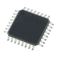
Vinculum-II VNC2-32L
FTDI Vinculum-II VNC2-32L Manuals
Manuals and User Guides for FTDI Vinculum-II VNC2-32L. We have
1
FTDI Vinculum-II VNC2-32L manual available for free PDF download: Manual
FTDI Vinculum-II VNC2-32L Manual (74 pages)
Embedded Dual USB Host Controller IC
Brand:
FTDI
| Category:
Controller
| Size: 2 MB
Table of Contents
Typical Applications
2
Part Numbers
2
USB Compliant
2
Table 1.1 Part Numbers
2
VNC2 Block Diagram
3
Figure 2.1 Simplified VNC2 Block Diagram
3
Table of Contents
4
Device Pin out and Signal Description Summary
7
Pin out - 32 Pin LQFP
7
Figure 3.1 32 Pin LQFP - Top down View
7
Pin out - 32 Pin QFN
8
Figure 3.2 32 Pin QFN - Top down View
8
Pin out - 48 Pin LQFP
9
Figure 3.3 48 Pin LQFP - Top down View
9
Pin out - 48 Pin QFN
10
Figure 3.4 48 Pin QFN - Top down View
10
Pin out - 64 Pin LQFP
11
Figure 3.5 64 Pin LQFP - Top down View
11
Pin out - 64 Pin QFN
12
Figure 3.6 64 Pin QFN - Top down View
12
VNC2 Schematic Symbol 32 Pin
13
Figure 3.7 Schematic Symbol 32 Pin
13
VNC2 Schematic Symbol 48 Pin
14
Figure 3.8 Schematic Symbol 48 Pin
14
VNC2 Schematic Symbol 64 Pin
15
Figure 3.9 Schematic Symbol 64 Pin
15
Pin Configuration USB and Power
16
Miscellaneous Signals
16
Table 3.1 USB Interface Group
16
Table 3.2 Power and Ground
16
Table 3.3 Miscellaneous Signal Group
16
Pin Configuration Input / Output
17
Table 3.4 Default I/O Configuration
18
Function Description
19
Key Features
19
Functional Block Descriptions
19
Embedded CPU
19
Flash Module
19
Flash Programming Module
19
Input / Output Multiplexer Module
19
Peripheral DMA Modules 0, 1, 2 & 3
20
RAM Module
20
Peripheral Interface Modules
20
USB Transceivers 0 and 1
20
USB Host / Device Controllers
20
12Mhz Oscillator
20
Table 4.1 - Peripheral Pin Requirements
20
Power Saving Modes and Standby Mode
21
O Multiplexer
22
Figure 5.1 IOBUS to Group Relationship-64 Pin
22
Figure 5.2 IOBUS to UART, SPI Slave0 and SPI Master Example
23
Figure 5.3 IOBUS to UART, SPI Slave0 and SPI Master Second Example
24
Figure 5.4 IOBUS to UART, SPI Slave0 and SPI Master Third Example
25
I/O Peripherals Signal Names
26
Table 5.1 I/O Peripherals Signal Names
26
I/O Multiplexer Configuration
27
Figure 5.5 VNC2 Toolchain App Wizard Showing Iomux Configuration
27
I/O Mux Group 0
28
I/O Mux Group 1
28
Table 5.2 Group 0
28
Table 5.3 Group 1
28
I/O Mux Group 2
29
I/O Mux Group 3
29
Table 5.4 Group 2
29
Table 5.5 Group 3
29
I/O Mux Interface Configuration Example
30
Figure 5.6 UART Example 64 Pin
30
Peripheral Interfaces
31
UART Interface
31
Figure 6.1 UART Receive Waveform
31
Figure 6.2 UART Transmit Waveform
31
UART Mode Signal Descriptions
32
Table 6.1 Data and Control Bus Signal Mode Options - UART Interface
32
Serial Peripheral Interface - SPI Modes
33
Table 6.2 SPI Signal Names
33
SPI Clock Phase Modes
34
Table 6.3 - SPI Slave Speeds
34
Table 6.4 - Clock Phase/Polarity Modes
34
Serial Peripheral Interface - Slave
35
Figure 6.3 - SPI CPOL CPHA Function
35
Figure 6.4 SPI Slave Block Diagram
35
SPI Slave Signal Descriptions
36
Full Duplex
36
Table 6.5 Data and Control Bus Signal Mode Options - SPI Slave Interface
36
Figure 6.5 Full Duplex Data Master Write
36
Table 6.6 SPI Command and Status Fields
37
Figure 6.6 Full Duplex Data Master Read
37
Figure 6.7 SPI Command and Status Structure
37
Half Duplex, 4 Pin
38
Figure 6.8 Half Duplex Data Master Write
38
Figure 6.9 Half Duplex Data Master Read
38
Half Duplex, 3 Pin
39
Figure 6.10 Half Duplex 3-Pin Data Master Write
39
Figure 6.11 Half Duplex 3-Pin Data Master Read
39
Unmanaged Mode
40
Figure 6.12 Unmanaged Mode Transfer Diagram
40
VNC1L Legacy Interface
41
Figure 6.13 VNC1L Mode Data Write
41
Figure 6.14 VNC1L Mode Data Read
41
Figure 6.15 VNC1L Compatible SPI Command and Status Structure
41
Table 6.7 SPI Command and Status Fields
42
Table 6.8 SPI Setup Bit Encoding
42
Table 6.9 SPI Slave Data Timing
43
Table 6.10 SPI Master Data Read Status Bit
43
Figure 6.16 SPI Slave Mode Timing
43
Table 6.11 SPI Master Data Write Status Bit
44
Figure 6.17 SPI Master Data Read (VNC2 Slave Mode)
44
Figure 6.18 SPI Slave Mode Data Write
44
Serial Peripheral Interface - SPI Master
45
Table 6.12 SPI Status Read Byte - Bit Descriptions
45
Figure 6.19 SPI Slave Mode Status Read
45
Figure 6.20 SPI Master Block Diagram
45
SPI Master Signal Descriptions
46
Table 6.13 SPI Master Signal Names
46
Table 6.14 SPI Master Timing
46
Debugger Interface
47
Debugger Interface Signal Description
47
Table 6.15 Debugger Signal Name
47
Figure 6.21 Typical SPI Master Timing
47
Parallel FIFO - Asynchronous Mode
48
FIFO Signal Descriptions
48
Read / Write Transaction Asynchronous FIFO Mode
49
Table 6.16 Data and Control Bus Signal Mode Options - Parallel FIFO Interface
49
Parallel FIFO - Synchronous Mode
50
Table 6.17 Asynchronous FIFO Mode Read / Write Timing
50
Figure 6.22 Asynchronous FIFO Mode Read / Write Cycle
50
Read / Write Transaction Synchronous FIFO Mode
51
Table 6.18 Synchronous FIFO Control Signals
51
Figure 6.23 Synchronous FIFO Mode Read / Write Cycle
51
General Purpose Timers
52
Pulse Width Modulation
52
Table 6.19 Synchronous FIFO Mode Read / Write Timing
52
General Purpose Input Output
53
Figure 6.24 PWM - Timing Diagram
53
Figure 6.25 GPIO Port Groups
53
USB Interfaces
54
Figure 7.1 USB Modes
54
Firmware
55
Rtos
55
Device Drivers
55
Firmware - Software Development Toolchain
55
Precompiled Firmware
56
Device Characteristics and Ratings
57
Absolute Maximum Ratings
57
DC Characteristics
57
Table 9.1 Absolute Maximum Ratings
57
Table 9.2 Operating Voltage and Current
57
ESD and Latch-Up Specifications
58
Table 9.3 I/O Pin Characteristics
58
Table 9.4 USB I/O Pin (USBDP, USBDM) Characteristics
58
Table 9.5 Crystal Oscillator 1.8 Volts DC Characteristics
58
Table 9.6 ESD and Latch-Up Specifications
58
Application Examples
59
Example VNC2 Schematic (MCU - UART Interface)
59
Figure 10.1 VNC2 Schematic (MCU - UART Interface)
59
Package Parameters
60
VNC2 Package Markings
60
Figure 11.1 Package Markings
60
Figure 11.2 Markings - 32 QFN
60
VNC2, LQFP-32 Package Dimensions
61
VNC2, QFN-32 Package Dimensions
61
Figure 11.3 LQFP-32 Package Dimensions
61
Figure 11.4 QFN-32 Package Dimensions
61
VNC2, LQFP-48 Package Dimensions
62
Figure 11.5 LQFP-48 Package Dimensions
62
VNC2, QFN-48 Package Dimensions
63
Figure 11. 6 QFN-48 Package Dimensions
63
VNC2, LQFP-64 Package Dimensions
64
Figure 11.7 64 Pin LQFP Package Details
64
VNC2, QFN-64 Package Dimensions
65
Figure 11.8 64 Pin QFN Package Details
65
Solder Reflow Profile
66
Figure 11.9 All Packages Reflow Solder Profile
66
Table 11.1 Reflow Profile Parameter Values
67
Table 11.2 Package Reflow Peak Temperature
67
Contact Information
68
Appendix A - References
69
Document References
69
Acronyms and Abbreviations
70
Appendix B - List of Figures and Tables
71
List of Tables
71
List of Figures
72
Appendix C - Revision History
74
Advertisement
Advertisement
Related Products
FTDI Vinculum-II VNC2-32Q
FTDI Vinculum II VNC2-32L1B
FTDI Vinculum II VNC2-32Q1B
FTDI Vinculum-II VNC2-64L
FTDI Vinculum-II VNC2-64Q
FTDI Vinculum-II VNC2-48L
FTDI Vinculum-II VNC2-48Q
FTDI Vinculum II VNC2-64L1B
FTDI Vinculum II VNC2-64Q1B
FTDI Vinculum II VNC2-48L1B
FTDI Categories
Controller
Computer Hardware
Remote Control
Motherboard
Cables and connectors
More FTDI Manuals
Login
Sign In
OR
Sign in with Facebook
Sign in with Google
Upload manual
Upload from disk
Upload from URL