Sign In
Upload
Manuals
Brands
Fastwel Manuals
Single board computers
CPB902
Fastwel CPB902 Manuals
Manuals and User Guides for Fastwel CPB902. We have
1
Fastwel CPB902 manual available for free PDF download: User Manual
Fastwel CPB902 User Manual (91 pages)
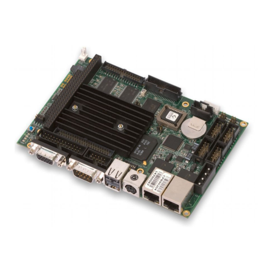
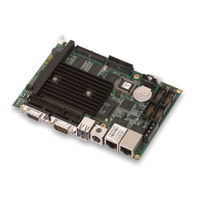
3.5" Highly Integrated Low Power SBC
Brand:
Fastwel
| Category:
Single board computers
| Size: 1 MB
Table of Contents
Table of Contents
3
List of Tables
5
List of Figures
6
Notation Conventions
7
General Safety Precautions
8
Unpacking, Inspection and Handling
9
Three Year Warranty
11
1 Introduction
12
Module Introduction
12
Figure 1.1: CPB902 Module Appearance
12
CPB902 Versions
13
Delivery Checklist
13
Additional Accessories
13
Table 1.1: CPB902 Versions
13
Table 1.2: CPB902 Supplied Set
13
Table 1.3: CPB902 Additional Accessories
13
Supplementary Information
14
Related Documents
14
Table 1.4: Related Publications
14
2 Technical Specifications
15
General
15
Power Requirements
16
Environmental
16
Mechanical
16
Dimensions and Weight
17
Mtbf
17
3 External Connections
18
Safety Regulations
18
Connection of Peripheral Devices
19
Figure 3.1: External Devices Connection
19
Compactflash Cards Installation
21
Figure 3.2: Cables 3 and 4 (Fig. 3.1) Connection for Console Operation
21
USB Devices Connection
21
Battery Replacement
22
Software Installation
22
4 Functional Description
23
Structure and Layout
23
Figure 4.1: CPB902 Block Diagram
23
Figure 4.2: Top Side: Connectors and Main Components Layout
25
Figure 4.3: Bottom Side: Connectors and Main Components Layout
25
Address Mapping
26
Memory Addressing
26
I/O Addressing
26
Table 4.1: Memory Address Mapping
26
Table 4.2: I/O Address Space
26
Table 4.3: System I/O Ports (FPGA)
28
Interrupt Settings
34
Figure 4.4: Interrupt Source Multiplexing Diagram
34
Table 4.4: Interrupt Settings
35
DMA Channels
36
Table 4.5: DMA Request Map
36
Figure 4.5: DMA Request Channels Multiplexing Diagram
36
Functional Description
37
Microprocessor
37
SDRAM Memory
37
Reserved Flash BIOS
37
UIDE Interface
38
Table 4.6: J1 HDD Connector Pinout
38
Compactflash Socket
39
Table 4.7: J2 Compact Flash Socket Pinout
39
NAND Flash
40
Video Controller and VGA/LCD Adapter Modules
40
Video Controller Operation Modes and Connection of Monitors
40
Table 4.8: S1 Settings: Display Type and Video Mode Selection
41
Table 4.9: Different Types of TFT/STN Panels Connection
42
Table 4.10: TFT/STN Panels Connector J16 Pinout
43
Figure 4.6: Connection of 16-Bit DSTN Panel
44
Figure 4.7: Connection of 24-Bit DSTN Panel
44
Table 4.11: LVDS Connector J21 Pinout
45
Figure 4.8: Connection of a TFT Panel with 1 Pixel Per FPSCLK Period
45
Figure 4.9: Connection of a TFT Panel with 2 Pixels Per FPSCLK Period
45
Figure 4.10: LVDS Interface for TFT LCD Panel
46
Figure 4.11: Panellink Interface for TFT LCD Panel
46
Table 4.12: P7 D-Sub VGA Connector Pinout
47
Figure 4.12: Panellink Interface for DSTN LCD Panel
47
CVM02: Sharp LQ104V1DG51 TFT Panel Connection
48
Table 4.13: CVM02 J2 Pin Assignments
48
Figure 4.13: Sharp LQ104V1DG51 TFT Panel Connection and Setup
48
CVM04: Sharp LQ104V1LG61 TFT Panel Connection
49
Figure 4.14: CV04 Unit Appearance
49
Figure 4.15: CVM04 Connections Diagram
50
Figure 4.16: LCD Screen Image Orientation Control
51
CVM01 Expansion Module
52
Figure 4.17: CVM01 Expansion Module
52
Keyboard and Mouse Interface
53
Table 4.14: CVM01 J5 Connector Pinout
53
Table 4.15: PS/2 Keyboard/Mouse Connector P5 Pinout
53
USB Interface
54
Fast Ethernet Interface
54
Serial Ports
54
Figure 4.18: IDC10 Pins Numbering
54
Table 4.16: Serial Ports Pin Assignments
55
Figure 4.19: COM3 - COM6 Ports Jumpers
55
Figure 4.20: Point-To-Point Connection of Two Modules in RS-422 Mode
56
Figure 4.21: Connection of Several Devices in RS-485 Mode
56
FDD/LPT Port
57
Figure 4.22: COM3-COM6 Ports: Simplified Interface Circuit Diagram
57
Table 4.17: LPT/FDD J15 Connector Pinout
58
LCD and Matrix Keyboard Port
59
LCD Connection
59
Figure 4.23: POWERTIP PC1604-A Alphanumeric LCD Connection Diagram
60
Figure 4.24: POWERTIP PG12864-A Graphics LCD Connection Diagram
60
Table 4.18: J17 Connector Pinout
61
Table 4.19: J18 Pinpad Pinout
61
Figure 4.25: J18 Pinpad Connection Circuit Diagram
61
Matrix Keypad Connection
62
Using Keyboard Interface by Discrete I/O Unit
62
Figure 4.26: Discrete I/O Channel Block Diagram
63
Figure 4.27: Discrete I/O Unit: Ports Binding Diagram
63
Optoisolated Reset/Interrupt
64
Table 4.20: J13 Settings: Switching Reset/Irq Source
64
Figure 4.28: Reset Source Selection and Optoisolated Input Circuit Diagram
64
FBUS Connector
65
RTC and Serial FRAM
65
J19 Configuration Jumpers
65
Table 4.21: FBUS Connector J22 Pinout
65
Table 4.22: J19 Pins Designation
65
Figure 4.29: J19 Circuit Diagram
65
PC/104 Header
66
Figure 4.30: PC/104 P4 Contacts Layout
66
Table 4.23: PC/104 P4 (Rows a and B) Contacts Designation
67
Table 4.24: PC/104 P4 (Rows C and D) Contacts Designation
68
Diagnostic Leds
69
Power Supply Connector
69
Table 4.25: CPB902 Diagnostic Leds Function
69
Table 4.26: J20 Power Connector Pinout
69
Overall and Mounting Dimensions
70
Figure 4.31: CPB902 Top Side: Overall and Mounting Dimensions
70
Figure 4.32: CPB902 Bottom Side: Overall and Mounting Dimensions
70
Mounting on a Panel
71
5 General Software® BIOS
72
BIOS Setup Program. Introduction
72
Main Menu
72
Table 5.1: Main Menu Items
73
Figure 5.1: Main Menu Screen Image
73
Basic CMOS Configuration
74
Table 5.2: Basic CMOS Configuration Menu Items
74
Figure 5.2: Basic CMOS Configuration Screen Image
74
Features Configuration
76
Table 5.3: Features Configuration Menu Items
76
Figure 5.3: Features Configuration Menu Screen
76
Custom Configuration
77
Table 5.4: Custom Configuration Menu Items
77
Figure 5.4: Custom Configuration Menu Screen
77
Pnp Configuration
80
Figure 5.5: Plug-N-Play Configuration Menu Screen Image
80
Shadow Configuration
81
Figure 5.6: Shadow Configuration Menu Screen Image
81
Manufacturing Link Mode
82
The Rest Main Menu Commands
83
Reset CMOS to Last Known Values
83
Reset CMOS to Factory Defaults
83
Write to CMOS and Exit
83
Exit Without Changing CMOS
83
Reset CMOS to Factory Defaults from a Remote PC
84
Extended BIOS Functions
84
User Programs Interface with FRAM Memory Units
84
User Leds Control
85
Superio Watchdog Timer Operation
86
ADM8697 Supervisor's Watchdog Timer Operation
87
Using INT 17H BIOS Extension to Control the Watchdog Timers
88
6 Appendices
90
Jumper Settings by Function
90
Table 6.1: Jumper Settings by Function
90
Jumper Settings by Assignment
91
Table 6.2: Jumper Settings by Assignment
91
Advertisement
Advertisement
Related Products
Fastwel CPC1600
Fastwel CPB8926
Fastwel CPB8929
FASTWEL CPB904
FASTWEL CPB904-02
FASTWEL CPB904-01
FASTWEL CPB904-03
Fastwel CPC514
Fastwel CPC522
Fastwel CPC1001
Fastwel Categories
Control Unit
Computer Hardware
Motherboard
Processor
Single board computers
More Fastwel Manuals
Login
Sign In
OR
Sign in with Facebook
Sign in with Google
Upload manual
Upload from disk
Upload from URL