Table of Contents
Advertisement
Quick Links
Advertisement
Table of Contents

Subscribe to Our Youtube Channel
Related Manuals for Fastwel CPB902

Summary of Contents for Fastwel CPB902
- Page 1 CPB902 3.5" Highly Integrated Low Power SBC User Manual Rev. 1.5b E May 2008...
- Page 2 Document name: CPB902 User Manual Manual version: 1.5b E Ref. doc. v.: 1.43 R + 1.08 + 1.11 + 1.12 (467444.014) Copyright © 2005, 2006, 2007, 2008 Fastwel Co. Ltd. All rights reserved. Revision Record Rev. Index Brief Description of Changes...
-
Page 3: Table Of Contents
List of Tables ..............................3 List of Figures ..............................4 Notation Conventions............................5 General Safety Precautions..........................6 Unpacking, Inspection and Handling........................7 Three Year Warranty............................9 Introduction.............................10 Module Introduction..........................10 CPB902 Versions..........................11 Delivery Checklist..........................11 Additional Accessories ..........................11 Supplementary Information........................12 1.5.1 Related Documents.......................12 Technical Specifications.........................13 General..............................13 Power Requirements..........................14 Environmental............................14... - Page 4 CPB902 4.3.7 Video Controller and VGA/LCD Adapter Modules..............38 4.3.7.1 Video Controller Operation Modes and Connection of Monitors ......38 4.3.7.2 CVM02: Sharp LQ104V1DG51 TFT Panel Connection...........46 4.3.7.3 CVM04: Sharp LQ104V1LG61 TFT Panel Connection ...........47 4.3.7.4 CVM01 Expansion Module ..................50 4.3.8 Keyboard and Mouse Interface....................51 4.3.9...
-
Page 5: List Of Tables
Table 4.23: PC/104 P4 (Rows A and B) Contacts Designation................65 Table 4.24: PC/104 P4 (Rows C and D) Contacts Designation ................66 Table 4.25: CPB902 Diagnostic LEDs Function .....................67 Table 4.26: J20 Power Connector Pinout.......................67 Table 5.1: Main Menu Items ..........................71 Table 5.2:... -
Page 6: List Of Figures
This document contains information, which is property of Fastwel Co. Ltd. It is not allowed to reproduce it or transmit by any means, to translate the document or to convert it to any electronic form in full or in parts without antecedent written approval of Fastwel Co. Ltd. or one of its officially authorized agents. -
Page 7: Notation Conventions
CPB902 Notation Conventions Warning, ESD Sensitive Device! This symbol draws your attention to the information related to electro static sensitivity of your product and its components. To keep product safety and operability it is necessary to handle it with care and follow the ESD safety directions. -
Page 8: General Safety Precautions
However, prolonged operation near the maximum temperature is not recommended by Fastwel or by electronic chip manufacturers due to thermal stress related failure mechanisms. These mechanisms are common to all silicon devices, they can reduce the MTBF of the product by increasing the failure probability. -
Page 9: Unpacking, Inspection And Handling
If damage is observed (usually in the form of bent component leads or loose socketed components), contact Fastwel's official distributor from which you have purchased the product for additional instructions. Depending on the severity of the damage, the product may even need to be returned to the factory for repair. - Page 10 In performing all necessary installation and application operations, please follow only the instructions supplied by the present manual. In order to keep Fastwel’s warranty, you must not change or modify this product in any way, other than specifically approved by Faswel or described in this manual.
-
Page 11: Three Year Warranty
If a product should fail through Fastwel's fault during the warranty period, it will be repaired free of charge. For out of warranty repairs, the customer will be invoiced for repair charges at current standard labor and materials rates. -
Page 12: Introduction
Introduction CPB902 Introduction This document presents general information on CPB902 processor module, the details of its proper and safe installation, configuration and operation. The issues of PC/104 modules and external devices connection are also considered. Module Introduction CPB902 processor module is a 3.5" highly integrated single board computer with full PC functionality. -
Page 13: Cpb902 Versions
Introduction CPB902 CPB902 Versions At the present time the CPB902 module is manufactured in two basic versions differing in SDRAM memory size and SVGA capability. Table 1.1: CPB902 Versions Version Decimal ID SDRAM Size SVGA CPB90204 467444.001 128 MB CPB90205 467444.002... -
Page 14: Supplementary Information
Introduction CPB902 Supplementary Information 1.5.1 Related Documents Information related to this product and its components can be found in the following documents: Table 1.4: Related Publications Product Publication CompactFlash cards CF+ and CompactFlash Specification Revision 1.4 Processor STPC Vega Programming manual... -
Page 15: Technical Specifications
Flash BIOS § 256 KB, reserved § In-system modification Solid State Disk § 16 MB with MS DOS-compatible Fastwel file system Storage: § Compact Flash Type I/II socket on board (bottom side) § Support for two UltraDMA/66 IDE devices Serial ports §... -
Page 16: Power Requirements
Technical Specifications CPB902 PS/2 § PS/2 keyboard and mouse interface § Floppy disk interface Parallel port § SPP/ECP/EPP compatible. Header, shared with FDD controller LCD Display and Matrix keyboard ports Connector for devices with FBUS interface Optoisolated Reset/IRQ input PC/104 Expansion Header Software Support: §... -
Page 17: Dimensions And Weight
Weight, not more: 0.22 kg MTBF MTBF for CPB902 is 120000 hours. The value is calculated according to: Telcordia Issue 1 model, Method I Case 3, for continuous operation at a surface location, at normal environmental conditions (Russian State Standard GOST 15150-69, "UHL4"... -
Page 18: External Connections
Safety Regulations The following safety regulations must be observed when installing or operating the module. Fastwel assumes no responsibility for any damage resulting from infringement of these rules. Warning! When handling or operating the module, special attention should be paid to the heatsink, because it can get very hot during operation. -
Page 19: Connection Of Peripheral Devices
External Connections CPB902 Connection of Peripheral Devices Figure 3.1: External Devices Connection CD-ROM Opto Reset 2.5" HDD PC/104 Connector SVGA Monitor Compact Flash Console (Remote PC) PS/2 Mouse J21 J22 PS/2 Key board COM6 COM4 COM3 COM5 Power On/Of f... - Page 20 The operating system is loaded from the on-board NAND Flash memory. Operating system on this flash-disk is FDOS supplemented with utilities. Before starting to work with CPB902 it is necessary to close the initially opened 1-2 jumper of J19 switch to enable the battery of the RTC for both versions of the module. See subsection 4.3.17...
-
Page 21: Compactflash Cards Installation
3.2.1 CompactFlash Cards Installation CompactFlash socket of CPB902 (J2) supports any 3.3 V or 5 V CompactFlash ATA type I/II cards. Carefully slide in the correctly oriented card and gently press to engage the contacts completely. To disengage the card, use the ejector button. -
Page 22: Battery Replacement
External Connections CPB902 3.2.3 Battery Replacement The lithium battery must be replaced with Panasonic BR2032 or a battery with similar characteristics. The expected life of a 190 mAh battery (Panasonic BR2032) is about 5 years. However, this typical value may vary because battery life depends on the operating temperature and the shutdown time of the system in which the battery is installed. -
Page 23: Functional Description
Functional Description CPB902 Functional Description Structure and Layout Functional diagram of the CPB902 module is shown in Figure 4.1. Figure 4.1: CPB902 Block Diagram IDC20 IDC40 MiniDIN-6 (1.27 mm) (1.27 mm) 2 pins IDC10 IDC44 (2 mm) DB15 Kbd / Mouse... - Page 24 DualApp and DualView modes support (under Windows 95/98/NT only) § LVDS interface Optoisolated remote Reset/IRQ input Layouts of main CPB902 components and connectors on top and bottom sides are presented in Figures 4.2 and 4.3 respectively. C P B 9 0 2 U s e r M a n u a l ©...
-
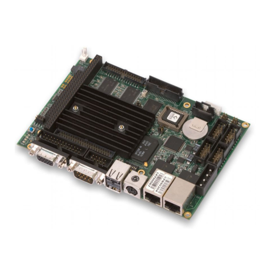
Page 25: Figure 4.2: Top Side: Connectors And Main Components Layout
Functional Description CPB902 Figure 4.2: Top Side: Connectors and Main Components Layout PS/2 Mouse, KBD COM1 COM2 Ethernet FDD/LPT Reset Button UIDE Reset +12V Selector Video COM3 COM4 Battery C0 D0 COM5 Speaker R154 COM6 B1 A1 COM3-COM6 Terminators FBUS... -
Page 26: Address Mapping
Functional Description CPB902 Address Mapping 4.2.1 Memory Addressing Table 4.1: Memory Address Mapping Address Range Size Description 00000h – 09FFFh 640 KB System memory A0000h – BFFFFh 128 KB Video memory C0000h – С7FFFh 32 KB Display BIOS memory BIOS extensions C8000h –... - Page 27 Functional Description CPB902 Base addresses of COM3-COM6 ports can be changed by bits 5, 6 of COM_ID identification register, the ID register address itself changes along with it. By default, the LPT port is set to ECP mode and has base address 378h.
-
Page 28: Table 4.3: System I/O Ports (Fpga)
Functional Description CPB902 Table 4.3: System I/O ports (FPGA) Port Read Write Value Comment (hex) NAND flash: read/write data, write address, write commands – FL_RB line status reading (NAND FLASH not available) /CE NAND FLASH line set to 0 /CE NAND FLASH line set to 1... - Page 29 Functional Description CPB902 Port Read Write Value Comment (hex) Switching DMA acknowledgement (DACENC=2) to /FDC_DACK2 line Switching DMA acknowledgement (DACENC=2) to /PC104_DACK2 line Switching DMA acknowledgement (DACENC=3) to /FBUS_DACK1 line Switching DMA acknowledgement (DACENC=3) to /PC104_DACK3 line Switching DMA acknowledgement (DACENC=5)
- Page 30 Functional Description CPB902 Port Read Write Value Comment (hex) FBUS unit: Disable interrupt on completion of transmission cycle FBUS unit: Enable interrupt on completion of transmission cycle FBUS unit: Disable interrupt on error FBUS unit: Enable interrupt on error –...
- Page 31 Functional Description CPB902 Port Read Write Value Comment (hex) Matrix keypad row 0: 0 – No key pressed 310.6=0 1 – Key pressed Write: Set status of the KEY_C2 discrete I/O channel trigger 310.6=1 (gray indicates trigger status after reset)
- Page 32 Functional Description CPB902 Port Read Write Value Comment (hex) LCD: read/write data, write commands, read status Always 1 LCD read available – – /lcd_cs2 line status lcd_e line status lcd_rs line status lcd_rw line status /lcd_cs1 line status KEY_R4 discrete I/O channel trigger status...
- Page 33 Functional Description CPB902 Port Read Write Value Comment (hex) EN_232_COM3 line status EN_232_COM4 line status EN_232_COM5 line status 31D* EN_232_COM6 line status – – – – FPGA registers (marked with *) access control. To allow access to FPGA registers it is necessary to write 55h to the port.
-
Page 34: Interrupt Settings
4.2.3 Interrupt settings By default, interrupts are generated by the devices belonging to the CPB902 module. The interrupt source multiplexing diagram is presented in Figure 4.4. Table 4.4 contains interrupt settings. Among the alternative interrupt generating devices are: expansion modules on ISA system bus (PC/104 connector), optoisolated Reset input, NAND flash memory, and keyboard. -
Page 35: Table 4.4: Interrupt Settings
Functional Description CPB902 Interrupt request configuration is performed in BIOS Setup, see description in sections and 5.6. Table 4.4: Interrupt Settings Default Source Alternative Source IRQ0 System timer – IRQ1 Keyboard (main port) Matrix keypad IRQ2 Cascading to IRQ9 –... -
Page 36: Dma Channels
Functional Description CPB902 4.2.4 DMA Channels Figure 4.5: DMA Request Channels Multiplexing Diagram Table 4.5: DMA Request Map DMA Channel Main Function Alternative Source Reserved for memory regeneration – PC/104 (DRQ1) – FDD (SIO) PC/104 (DRQ2) FBUS PC/104 (DRQ3) Slave controller –... -
Page 37: Functional Description
4.3.3 Reserved Flash BIOS The CPB902 takes advantage of flash-memory based BIOS. Flash BIOS storage capacity is 512 KB. The main (working) copy of BIOS occupies 256 KB, the rest 256 KB is used for reserve BIOS copy. Reserve BIOS is enabled by closing pins 3-4 at the J19 pinpad. -
Page 38: Uide Interface
(3.5" HDD, CD-ROM) having 40-contact 2.5 mm pitch connector can be connected to CPB902 via the CDM02 adapter. This adapter is connected to the 40-pin contact connector of the IDE device, and with the ACS00010 FC44 cable to CPB902 J1 connector. -
Page 39: Compactflash Socket
4.3.5 CompactFlash Socket CompactFlash Type I/II cards can be connected to J2 socket on the bottom side of CPB902. The device in this socket will be detected by the system as Secondary Master disk drive. This device can be assigned as a bootable disk in BIOS Setup program. The pinout of the J2 socket is presented in the following table. -
Page 40: Nand Flash
Functional Description CPB902 4.3.6 NAND Flash The capacity of the on-board NAND flash memory chip is 16 MB. It can be used as a bootable disk or can be disabled in BIOS Setup (see section 5.3 for details). 4.3.7 Video Controller and VGA/LCD Adapter Modules 4.3.7.1... -
Page 41: Table 4.8: S1 Settings: Display Type And Video Mode Selection
Functional Description CPB902 The S1 DIP-switch allows to choose video mode for the display. Power on enables the selected mode. The table below presents available display types and video controller operation modes. "0" corresponds to "ON" position, "1" to "OFF". -
Page 42: Table 4.9: Different Types Of Tft/Stn Panels Connection
Functional Description CPB902 The module's video controller supports color STN and TFT panels with digital interface. These panels are connected to J16 connector (AMP 147377-4, counterpart АМР 111196-9). Color TFT panels with RGB interface are also supported. Correspondence between the video controller interface lines (FDATA[23…0]) and TFT/STN panels' interfaces is given in table 4.9 below. -
Page 43: Table 4.10: Tft/Stn Panels Connector J16 Pinout
Functional Description CPB902 Table 4.10: TFT/STN Panels Connector J16 Pinout Pin # Signal Pin # Signal FDATA16 LVDS_MCKIN FDATA17 VBIASEN FDATA18 FPVDDEN FDATA19 FDATA0 FDATA20 FDATA1 FDATA21 FDATA2 FDATA22 FDATA3 FDATA23 FDATA4 FPEN FDATA5 FDATA6 FPSCLK FDATA7 FVSYNC FDATA8 FDATA9... -
Page 44: Figure 4.6: Connection Of 16-Bit Dstn Panel
Functional Description CPB902 Figure 4.6: Connection of 16-bit DSTN Panel panel power control circuitry Figure 4.7: Connection of 24-bit DSTN Panel panel power control circuitry C P B 9 0 2 U s e r M a n u a l ©... -
Page 45: Table 4.11: Lvds Connector J21 Pinout
Functional Description CPB902 Figure 4.8: Connection of a TFT Panel with 1 Pixel per FPSCLK Period 1 pixel/clock panel power control circuitry Figure 4.9: Connection of a TFT Panel with 2 Pixels per FPSCLK Period TFT Panel 2 pixels/clock panel power... -
Page 46: Figure 4.10: Lvds Interface For Tft Lcd Panel
Functional Description CPB902 Figure 4.10: LVDS Interface for TFT LCD Panel Data Pairs TxOut0 RxIn0 RxOut R[7:0] RxOut G[7:0] TxOut1 RxIn1 RxOut B[7:0] TxOut2 RxIn2 RxOut HSYNC RxOut VSYNC TxOut3 RxIn3 RxOut LVDS Clock TxCLKOut RxCLKIn RxCLKOut FPSC TFT LCD Panel Figure 4.11:... -
Page 47: Table 4.12: P7 D-Sub Vga Connector Pinout
Functional Description CPB902 Figure 4.12: PanelLink Interface for DSTN LCD Panel PanelLink Transmitter PanelLink Receiver DSTN Sil100 Sil100 LCD Panel U[11:0] TxIn TxOut0 RxIn0 RxOut U[11:0] L[11:0] TxIn RxOut L[11:0] TxOut1 RxIn1 FHSYNC TxIn TxOut2 RxIn2 RxOut HSYNC FVSYNC TxIn... -
Page 48: Cvm02: Sharp Lq104V1Dg51 Tft Panel Connection
The CVM02 adapter card has a J2 pinpad used to set display orientation on the panel screen and for backlight control. The diagram on the figure below shows how this panel type is connected to CPB902. Figure 4.13: Sharp LQ104V1DG51 TFT Panel Connection and Setup... -
Page 49: Cvm04: Sharp Lq104V1Lg61 Tft Panel Connection
CVM04: Sharp LQ104V1LG61 TFT Panel Connection CVM04 module is designed to serve as an intermediate device to connect Sharp LQ104V1LG61 or similar LCD panel to Fastwel CPB90204 processor module. CVM04 functions as an adapter module between LVDS connector of processor module and LCD panel. -
Page 50: Figure 4.15: Cvm04 Connections Diagram
Functional Description CPB902 Figure 4.15: CVM04 Connections Diagram FAPI.685611.092 Cable L = 70 mm LQ104V1LG61 FAPI.685612.037 Cable L = 800 mm CPB90204 Power Supply CN3 CN2 +5 V, +12 V CV04 FAPI.685612.015-02 Cable DC/AC PS-DA0253-03 To connect LQ104V1LG61 LCD panel to СРВ90204 processor module follow the procedure below. -
Page 51: Figure 4.16: Lcd Screen Image Orientation Control
Functional Description CPB902 CVM04 is equipped with components enabling following additional functions. Backlight Lamps Brightness Control An adjustable resistor R2 is installed on the module. R2 allows to adjust the brightness of LCD backlight lamps through changing its resistance according to PS-DA0253-03 DC/AC converter specification. -
Page 52: Cvm01 Expansion Module
CVM01 Expansion Module TFT-Panels Connection Discrete Input The CVM01 P1 VGA connector has the same pin assignments as CPB902 P7 connector (see Pinout Table in subsection 4.3.7.1). The pinout of CVM01 J5 connector is given in the table below. CVM01 provides possibility to adjust the display driver power voltage (VEEP) with R5 potentiometer, and to set the digital interface power voltage with J2-J4 jumpers. -
Page 53: Keyboard And Mouse Interface
4.3.8 Keyboard and Mouse Interface CPB902 is provided with a 6-contact PS/2 mini-DIN connector (P5) for mouse and/or keyboard. Simultaneous connection of mouse and keyboard is possible via Y-cable. If mouse is not used, a keyboard is directly connected to P5 connector. -
Page 54: Usb Interface
4.3.11 Serial Ports The CPB902 is furnished with six serial ports. COM1 and COM2 ports have standard PC AT base addresses. The base address of COM3 – COM6 group of ports can be changed. COM1 is routed to J4 IDC10 connector (2.54 mm pitch). It has only three lines (RXD, TXD and GND) and is intended for console operation and file exchange. -
Page 55: Table 4.16: Serial Ports Pin Assignments
Functional Description CPB902 Table 4.16: Serial Ports Pin Assignments COM2 COM1 COM3/COM4/COM5/COM6 Pin # RS-232 RS-232 RS-232 RS-422 RS-485 – – – – – – – – – – – – – – – – – – COM2, COM3 – COM6 ports have ESD and overload protection. COM1 port has no protection. -
Page 56: Figure 4.20: Point-To-Point Connection Of Two Modules In Rs-422 Mode
Functional Description CPB902 Figure 4.20: Point-to-Point Connection of Two Modules in RS-422 Mode IDC10 Connector (J5/J7/J9/J11) RS422/RS485 RS422/RS485 Converter Converter Figure 4.21: Connection of Several Devices in RS-485 Mode Terminating IDC10 Connector Module (J5/J7/J9/J11) RS422/RS485 Converter Peripheral Module RS485 Converter... -
Page 57: Fdd/Lpt Port
4.3.12 FDD/LPT Port The LPT1 port of CPB902 supports EPP and ECP operation modes. ECP is the default mode. LPT is routed to J15 connector shared with FDD port. Switching between LPT and FDD ports is performed in BIOS Setup. -
Page 58: Table 4.17: Lpt/Fdd J15 Connector Pinout
Functional Description CPB902 Table 4.17: LPT/FDD J15 Connector Pinout Pin # LPT1 Signals FDD Signals /STROBE /DS0 /ALF /DRVDEN0 /INDEX /ERROR /HDSEL /TRK0 /INIT /DIR /SLCTIN /STEP /RDATA /DSKCHG – /MTR0 – /ACK /DS1 BUSY /MTR1 WDATA SLCT WGATE C P B 9 0 2... -
Page 59: Lcd And Matrix Keyboard Port
CPB902 4.3.13 LCD and Matrix Keyboard Port LCD monitors and matrix keypads share J17 header on the top side of CPB902 processor module. 4.3.13.1 LCD Connection The CPB902 connector J17 is used for connection of LCD monitors based on HD44780, S6A0069, S6B0108 or compatible controllers. -
Page 60: Figure 4.23: Powertip Pc1604-A Alphanumeric Lcd Connection Diagram
Functional Description CPB902 Figure 4.23: POWERTIP PC1604-A Alphanumeric LCD Connection Diagram Signal Contact LCD Contact Signal J17.14 J17.15 LCD_TRIM* J17.16 LCD_RS J17.17 LCD_R/W J17.18 R/#W LCD_E J17.19 LCD_D0 J17.20 LCD_D1 J17.21 LCD_D2 J17.22 LCD_D3 J17.23 LCD_D4 J17.24 LCD_D5 J17.25 LCD_D6 J17.26... -
Page 61: Table 4.18: J17 Connector Pinout
Functional Description CPB902 J17 connector pinout is given in Table 4.18. Table 4.19 presents designation of contacts of the J18 pinpad, which is used to set the LCD driver power voltage. Table 4.18: J17 Connector Pinout Pin # Function Pin #... -
Page 62: Matrix Keypad Connection
16 (4х4), 20 (4х5 or 5х4), 25 (5х5), 30 (6х5 or 5х6) or 36 (6х6) keys. To interface with a keypad CPB902 has two ports in I/O address area – one is column scanning and interrupt control port, another one is row scanning port. -
Page 63: Figure 4.26: Discrete I/O Channel Block Diagram
Functional Description CPB902 Figure 4.26: Discrete I/O Channel Block Diagram Output port (T rigger) FPGA 315h, 316h (W) 316h, 31Bh (R) +5 V (max) Load Input port 315h, 316h (R) = 20 mА Figure 4.27: Discrete I/O Unit: Ports Binding Diagram... -
Page 64: Optoisolated Reset/Interrupt
Functional Description CPB902 4.3.14 Optoisolated Reset/Interrupt The module has one optoisolated discrete input J14, which can be used for remote reset or for interrupt generation. This interrupt is served by IRQ14 line of the interrupt controller. Use J13 jumpers to select the microprocessor reset source and to enable the interrupt generation by the signal from the optoisolated input. -
Page 65: Fbus Connector
4.3.15 FBUS Connector FBUS is an interface bus, which enables CPB902 to be a part of FBUS networks. FBUS interface controller is routed to J22 (one row, 6-pin, 2 mm pitch) on-board connector. FBUS physical level is identical to the one of RS485 interface. The addresses 0x312–0x314 are used to manipulate the FBUS controller. -
Page 66: Pc/104 Header
4.3.18 PC/104 Header P4 header mounted on CPB902 allows connection of PC/104 expansion modules. The processor module can accommodate 3 PC/104 expansion modules maximum. The contact configuration of P4 header is shown in Figure 4.30. Tables 4.23 and 4.24 give the designation of P4 contacts. -
Page 67: Table 4.23: Pc/104 P4 (Rows A And B) Contacts Designation
Functional Description CPB902 Table 4.23: PC/104 P4 (Rows A and B) Contacts Designation Pin # Signal In/Out Pin # Signal In/Out /IOCHK – Power In/Out RESET In/Out Power In/Out IRQ9 In/Out – In/Out DRQ2 In/Out -12V Power In/Out In/Out +12V... -
Page 68: Table 4.24: Pc/104 P4 (Rows C And D) Contacts Designation
Functional Description CPB902 Table 4.24: PC/104 P4 (Rows C and D) Contacts Designation Pin # Signal In/Out Pin # Signal In/Out /SBHE /MEMCS16 LA23 /IOCS16 LA22 IRQ10 LA21 IRQ11 LA20 IRQ12 LA19 IRQ13 LA18 IRQ14 LA17 /DACK0 /MEMR DRQ0 /MEMW... -
Page 69: Diagnostic Leds
The power is supplied to CPB902 via J20 connector. The main power voltage of the processor module is +5V. +12 V is supplied via J20 connector, but is not used in CPB902. It is routed to P4 PC/104 connector. The PC/104 connector contacts corresponding to -5 V and -12 V voltages are not connected to the board circuitry. -
Page 70: Overall And Mounting Dimensions
Functional Description CPB902 Overall and Mounting Dimensions Figure 4.31: CPB902 Top Side: Overall and Mounting Dimensions 27 m ax 148 max 1.5* 85.9 Ф3 7 openings А Ф1.9 2 op. C0 D0 B1 A1 10.9 Figure 4.32: CPB902 Bottom Side: Overall and Mounting Dimensions A (Heat-conducting Plate View) М3* Two openings... -
Page 71: Mounting On A Panel
4.4.1 Mounting on a Panel It is possible to provide additional heat removal, when CPB902 is installed on a metallic mounting panel using 9 mm high stud spacers. For better heat transfer results use thermal paste or heat- conducting pad. -
Page 72: General Software® Bios
CPB902 General Software® BIOS The General Software® BIOS in CPB902 is an adapted version of a standard BIOS for IBM PC AT-compatible personal computers equipped with Intel®x86 and compatible processors. BIOS provides low-level support for the central processing, memory, and I/O system units. -
Page 73: Table 5.1: Main Menu Items
RAM on module initialization. Start RS232 Manufacturing Link This menu item starts the service mode, which allows to explore the disk drives of the CPB902 from a remote PC using a RS232 link between the module and a remote PC (see section 5.8). -
Page 74: Basic Cmos Configuration
General Software® BIOS CPB902 Basic CMOS configuration On selection of this Main menu item the following screen is shown: Figure 5.2: Basic CMOS Configuration Screen Image ╔══════════════════════════════════════════════════════════════════════════════╗ ║ ║ System BIOS Setup - Basic CMOS Configuration ║ ║ (C) 2005 General Software, Inc. All rights reserved ╠══════════════════════════════════════════════════════════════════════════════╣... - Page 75 General Software® BIOS CPB902 Menu Item Function IDE DRIVE GEOMETRY: IDE disk drive geometry selection for Primary Master (IDE0 Master), Primary Slave (IDE0 Slave) and Secondary Master (IDE1 Master, Compact Flash). IDE0 Master Options: IDE0 Slave Not installed – disk drive not connected;...
-
Page 76: Features Configuration
General Software® BIOS CPB902 Features Configuration Features Configuration menu screen is shown on the following figure: Figure 5.3: Features Configuration Menu Screen ╔══════════════════════════════════════════════════════════════════════════════╗ ║ ║ System BIOS Setup - Features Configuration ║ ║ (C) 2005 General Software, Inc. All rights reserved ╠═══════════════════════════════════════╤══════════════════════════════════════╣... -
Page 77: Custom Configuration
General Software® BIOS CPB902 Custom Configuration Custom Configuration menu screen is shown on the following figure: Figure 5.4: Custom Configuration Menu Screen ╔══════════════════════════════════════════════════════════════════════════════╗ ║ ║ System BIOS Setup - Custom Configuration ║ ║ (C) 2005 General Software, Inc. All rights reserved ╠═══════════════════════════════════════╤══════════════════════════════════════╣... - Page 78 General Software® BIOS CPB902 Menu Item Options Description NMI Source Disabled If enabled, connects the PFO signal to NMI. PFO (Power Fail Output) signal is issued by a supervisor Enabled if power voltage becomes lower than nominal value. СОМ3...СОМ6 ports base address selection COM3…COM6...
- Page 79 General Software® BIOS CPB902 Menu Item Options Description DRQ2 DMA channel is used by floppy disk controller PC/104 DMA channel is available for external devices via PC/104 interface Remember! Wrong or incorrect settings may lead to abnormal system performance. To correct possible errors, restart the BIOS Setup program and restore manufacturer's settings by selection of “Reset CMOS to factory defaults”...
-
Page 80: Pnp Configuration
General Software® BIOS CPB902 PnP Configuration This BIOS Setup section provides access to Plug-and-Play related IRQ and DMA assignments. The menu screen is shown in the figure below. Figure 5.5: Plug-n-Play Configuration Menu Screen Image ╔══════════════════════════════════════════════════════════════════════════════╗ ║ ║ System BIOS Setup - Plug-n-Play Configuration ║... -
Page 81: Shadow Configuration
General Software® BIOS CPB902 Shadow Configuration The figure below presents the Shadow Configuration menu screen. Figure 5.6: Shadow Configuration Menu Screen Image ╔══════════════════════════════════════════════════════════════════════════════╗ ║ ║ System BIOS Setup - Shadow/Cache Configuration ║ ║ (C) 2005 General Software, Inc. All rights reserved ╠══════════════════════════════════════════════════════════════════════════════╣... -
Page 82: Manufacturing Link Mode
D: and E: corresponding to the devices A: and C: of the module will appear on the PC. Manufacturing Link mode can also be used for formatting of the CPB902 disks and transferring of MS DOS or FDOS 6.22 operating systems. -
Page 83: The Rest Main Menu Commands
General Software® BIOS CPB902 The Rest Main Menu Commands 5.9.1 Reset CMOS to last known values If you changed your mind and decided not to write the changes you have made in BIOS Setup program and have not yet saved the values in CMOS memory, you may select this command to return to the last saved parameters (i.e. -
Page 84: Reset Cmos To Factory Defaults From A Remote Pc
CMOS_RST.COM is a software utility, which allows to reset the BIOS setup parameters stored in CMOS memory to factory defaults from a remote PC. To do so, follow the procedure below. Connect COM1 port of CPB902 to a PC COM port with a null-modem cable; Start CMOS_RST.COM on a remote PC with the parameter: CMOS_RST.COM COM2... -
Page 85: User Leds Control
General Software® BIOS CPB902 5.11.2 User LEDs Control USER_LED1 and USER_LED2 user LEDs are switched on and off by writing logical 1 or 0 respectively to GPIO4 and GPIO5 lines of the GPIO processor unit. Sample LED control program code fragments are given below. -
Page 86: Superio Watchdog Timer Operation
General Software® BIOS CPB902 5.11.3 SuperIO Watchdog Timer Operation The SuperIO FDC37B787 internal WDT has software adjustable (programmable) timeout period from 1 second up to 255 minutes. Upon expiry of the timeout the RESET signal is issued by the WDT, unless it is reset by the user program. Sample program code fragments setting and clearing the WDT are given below. -
Page 87: Adm8697 Supervisor's Watchdog Timer Operation
General Software® BIOS CPB902 5.11.4 ADM8697 Supervisor's Watchdog Timer Operation This watchdog timer has fixed timeout period from 4.5 to 10.5 seconds depending on supervisor chip parameters. Upon expiry of the timeout the WDT resets the system, unless it is reset by the user program. -
Page 88: Using Int 17H Bios Extension To Control The Watchdog Timers
General Software® BIOS CPB902 5.11.5 Using INT 17H BIOS Extension to Control the Watchdog Timers INT 17H extensions which allow to access the watchdog timers and to support their operation are described below. SIO WDT1 control ▪ WDT1 enable; Input parameters: AH=11h;... - Page 89 General Software® BIOS CPB902 To control the WDT2 the OCTAGON interface can be used as well: ▪ Enable WDT2 Input parameters: AX=0FD01h; DX=0FFFFh. ▪ WDT2 strobing Input parameters: AX=0FD02h4 DX=0FFFFh. ▪ Disable WDT2 Input parameters: AX=0FD03h; DX=FFFFh. INT17H call Input parameters: AH=0Fh;...
-
Page 90: Appendices
Appendices CPB902 Appendices Jumper Settings by Function Table 6.1: Jumper Settings by Function Function Jumper Short Description (*) Enable terminator between TX+ and TX- lines of COM3 port in RS422 J6: 1-2 mode Terminators on COM3 in RS-422/RS-485 modes Enable terminator between RX+ and RX- lines of COM3 port in RS422... -
Page 91: Jumper Settings By Assignment
Appendices CPB902 Jumper Settings by Assignment Table 6.2: Jumper Settings by Assignment Jumper Assignment J13: 1-2 Enable module reset by supervisor's WDT J13: 3-4 Enable module reset by SIO WDT J13: 5-6 Enable module reset by optoisolated input signal J13: 7-8...
Need help?
Do you have a question about the CPB902 and is the answer not in the manual?
Questions and answers