Sign In
Upload
Manuals
Brands
Diamond Systems Manuals
Motherboard
Poseidon
Diamond Systems Poseidon Manuals
Manuals and User Guides for Diamond Systems Poseidon. We have
1
Diamond Systems Poseidon manual available for free PDF download: User Manual
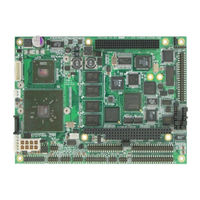
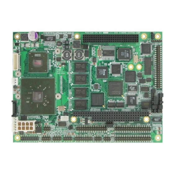
Diamond Systems Poseidon User Manual (118 pages)
EPIC format VIA CPU Board with Integrated Data Acquisition
Brand:
Diamond Systems
| Category:
Motherboard
| Size: 1 MB
Table of Contents
Table of Contents
2
Poseidon User Manual Page
3
Poseidon User Manual Page
4
Poseidon User Manual Page
5
Poseidon User Manual Page
6
Introduction
7
Description and Features
7
Analog Output
8
Block Diagram
9
Figure 1: Poseidon Functional Block Diagram
9
Functional Overview
10
Data Acquisition
11
Board Description
13
Figure 2: Poseidon Board Layout
13
Connector Summary
14
Jumper Summary
14
Connectors
15
PC/104 ISA Bus
15
Figure 3: CN6 and CN7 Connectors
15
PC/104-Plus PCI Bus
16
Figure 4: CN3 Connector
16
PS2 Mouse and Keyboard Connector
17
Utility Connector
17
Data Acquisition (Digital I/O) Connector
19
Data Acquisition (Analog I/O) Connector
20
Ethernet Connector
21
Audio I/O Connector
21
Speaker Connector
22
External Auxiliary Power Connector (Output)
23
Figure 5: CN10 Connector
23
IDE Connector
24
Serial Port I/O Connector
25
External Battery Connector
27
Figure 6: CN8 Connector
27
LCD Panel (LVDS Interface) Connector
28
Figure 7: LCD Panel Connector
28
VGA Connector
29
LCD Backlight Connector
30
Power Input Connector
30
Figure 8: CN4 Connector
30
Figure 9: CN9 Connector
30
USB 2.0 Connectors
31
Serial ATA Connector
32
Figure 10: Serial ATA Connector
32
I/O Panel Power
33
Standard JTAG Configuration Interface (Factory Use)
34
Reference Voltage Test Point (Factory Use)
34
Board Configuration
35
PCI VI/O Voltage Setting (JP1)
36
Figure 11: Jumper Block JP1
36
Figure 12: JP1 Settings
37
DAQ Configuration (JP2)
38
Figure 13: Base Address Configuration Example
38
Figure 14: DMA Channel Selection
38
COM3/COM4/ADC IRQ Configuration (JP3)
39
Figure 15: Bus Width Configuration
39
Analog I/O Single-Ended/Differential Configuration (JP4)
40
Figure 16: IRQ Selection Example
40
DAC Configuration (JP5)
41
Figure 17: Analog I/O Single-Ended/Differential Configuration Example
41
Figure 18: JP5 Jumper Block
41
Battery Connection (JP6)
42
Figure 19: D/A Configuration for ±5V Output Range Example
42
Figure 20: D/A Configuration to Reset to Zero Scale Example
42
Figure 21: JP6 Jumper
42
ATX Power Control (JP7)
43
Figure 22: ATX Configuration Using JP7
43
RS-422/RS-485 Termination Configuration (JP8)
44
DIO Pull-Up/Pull-Down Configuration (JP9)
44
Figure 23: RS-422/RS-485 Termination Configuration Options
44
Figure 24: DIO Pull-Up/Pull-Down Configuration
44
System Features
45
System Resources
45
Console Redirection to a Serial Port
45
Flash Memory
46
Backup Battery
46
System Reset
47
On-Board Video
47
System I/O
48
Ethernet
48
Serial Ports
48
PS/2 Ports
49
USB Ports
49
Figure 25: Data Acquisition Block Diagram
51
Data Acquisition Circuitry I/O Map
52
I/O Register Summary
54
I/O Register Definitions
56
Data Acquisition Circuit
51
Enabling Enhanced Features
77
Enhanced Mode
77
Normal Mode
77
Analog-To-Digital Input Ranges and Resolution
78
Overview
78
Unipolar and Bipolar Inputs
78
Input Ranges and Resolutions
78
A/D Conversion Formulas
79
Performing an A/D Conversion
81
Select the Input Channel
81
Select the Input Range
82
Wait for Analog Input Circuit to Settle
82
Perform an A/D Conversion on the Current Channel
82
Wait for the Conversion to Finish
82
Read the Data from the Board
82
Convert the Numerical Data to a Meaningful Value
83
A/D Sampling Methods
84
Sampling Modes
84
FIFO Description
85
Scan Sampling
85
Sequential Sampling
85
How to Perform Conversions Using Interrupts
86
Analog Output Ranges and Resolution
87
Description
87
Resolution
87
Full-Scale Range Selection
87
Digital-To-Analog Conversion
88
Compute the D/A Output Value for the Desired Output Voltage
88
Compute the LSB and MSB Values
88
Add the Channel Number to the MSB
89
Set D/A Simultaneous Update Bit
89
Write the LSB and MSB to the Board
89
Monitor the DACBUSY Status Bit
89
Waveform Generator
91
Description
91
Programming the D/A Waveform Generator
91
Auto-Calibration
93
Background
93
Performing Auto-Calibration with Software
94
Performing Auto-Calibration with Dspic
94
Digital I/O Operation
95
Main Digital I/O Internal 82C55 Circuit
95
Auxiliary Digital I/O
96
Counter/Timer Operation
98
Counter/Timer Features and Configuration Options
98
Counter/Timer Configuration
98
Counter/Timer Access and Programming
98
Watchdog Timer Programming
99
Flashdisk Module
101
Installing the Flashdisk Module
101
Figure 26: Flashdisk Module
101
Using the Flashdisk with Another IDE Drive
102
Power Supply
102
Figure 27: Flashdisk Programmer Board Layout
103
Flashdisk Programmer Board
103
I/O Cables
104
PNL-PSD Panel I/O Board for Poseidon CPU
105
Mounting PC/104-Plus Cards Onto a Poseidon Baseboard
105
Jumper Configuration
106
Customization Options
113
Specifications
114
Cpu
114
Data Acquisition Circuitry
114
Power Supply
115
General
115
Additional Information
116
Appendix A. COM3/4/ADC IRQ Configuration for First Release Boards, Rev A1
117
Technical Support
118
Advertisement
Advertisement
Related Products
Diamond Systems PGS800-256
Diamond Systems PGS800-256-2G
Diamond Systems PCI/104-Express QSeven
Diamond Systems PLT-T56N-4G
Diamond Systems PLT-T56N-2G
Diamond Systems PLT-T40N-4G
Diamond Systems PLT-T40N-2G
Diamond Systems PLT-3845XT-8G
Diamond Systems PLT-3845XT-4G
Diamond Systems PLT-3845XT-2G
Diamond Systems Categories
Motherboard
Carrier boards
Computer Hardware
Power Supply
Control Unit
More Diamond Systems Manuals
Login
Sign In
OR
Sign in with Facebook
Sign in with Google
Upload manual
Upload from disk
Upload from URL