Sign In
Upload
Manuals
Brands
Cypress Manuals
Microcontrollers
FM4 Series
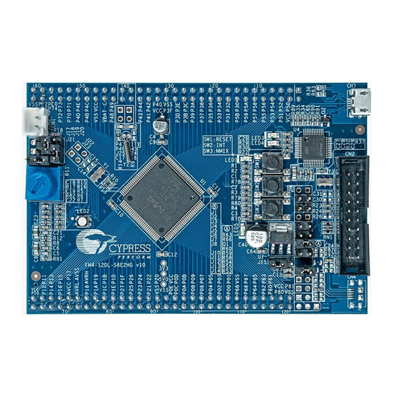
User Manuals: Cypress FM4 Series Microcontrollers
Manuals and User Guides for Cypress FM4 Series Microcontrollers. We have
1
Cypress FM4 Series Microcontrollers manual available for free PDF download: Peripheral Manual
Cypress FM4 Series Peripheral Manual (1102 pages)
32-Bit
Brand:
Cypress
| Category:
Microcontrollers
| Size: 13 MB
Table of Contents
Table of Contents
10
CHAPTER 1: System Overview
23
Bus Architecture
24
Bus Block Diagram
26
Memory Architecture
27
Memory Map
28
Peripheral Address Map
29
Cortex-M4F Architecture
32
Option Configuration
35
Mode
36
CHAPTER 2-1: Clock
37
Clock Generation Unit Overview
38
Clock Generation Unit Configuration/Block Diagram
39
Clock Generation Unit Operations
44
Selecting the Clock Mode
44
Internal Bus Clock Frequency Division Control
45
PLL Clock Control
46
Oscillation Stabilization Wait Time
48
Interrupt Factors
49
Clock Gear Function
50
Clock Setup Procedure Examples
52
List of Clock Generation Unit Registers
58
System Clock Mode Control Register (SCM_CTL)
59
System Clock Mode Status Register (SCM_STR)
61
Base Clock Prescaler Register (BSC_PSR)
62
APB0 Prescaler Register (APBC0_PSR)
63
APB1 Prescaler Register (APBC1_PSR)
64
APB2 Prescaler Register (APBC2_PSR)
65
Software Watchdog Clock Prescaler Register (SWC_PSR)
66
Trace Clock Prescaler Register (TTC_PSR)
67
Clock Stabilization Wait Time Register (CSW_TMR)
68
PLL Clock Stabilization Wait Time Setup Register (PSW_TMR)
69
PLL Control Register 1 (PLL_CTL1)
70
PLL Control Register 2 (PLL_CTL2)
71
Debug Break Watchdog Timer Control Register (DBWDT_CTL)
72
Interrupt Enable Register (INT_ENR)
73
Interrupt Status Register (INT_STR)
74
Interrupt Clear Register (INT_CLR)
75
PLL Clock Gear Control Register (PLLCG_CTL)
77
Clock Generation Unit Usage Precautions
79
CHAPTER 2-2: Peripheral Clock Gating
81
Peripheral Clock Gating Overview
82
Peripheral Clock Gating Configuration
85
Peripheral Clock Gating Control
87
Peripheral Clock Control Procedures
88
Peripheral Clock Gating Function Registers
91
Peripheral Function Clock Control Register 0 (CKEN0)
92
Peripheral Reset Control Register 0 (MRST0)
95
Peripheral Clock Control Register 1 (CKEN1)
97
Peripheral Function Reset Control Register 1 (MRST1)
99
Peripheral Clock Control Register 2 (CKEN2)
101
Peripheral Function Reset Control Reset 2 (MRST2)
105
Peripheral Clock Gating Function Usage Precautions
109
CHAPTER 2-3: High-Speed CR Trimming
113
High-Speed CR Trimming Function Overview
114
High-Speed CR Trimming Function Configuration and Block Diagram
115
High-Speed CR Trimming Function Operation
116
High-Speed CR Trimming Function Setup Procedure Example
117
High-Speed CR Trimming Function Register List
124
High-Speed CR Oscillation Frequency Division Setup Register (MCR_PSR)
125
High-Speed CR Oscillation Frequency Trimming Register (MCR_FTRM)
126
High-Speed CR Oscillation Temperature Trimming Setup Register (MCR_TTRM)
127
High-Speed CR Oscillation Register Write-Protect Register (MCR_RLR)
128
High-Speed CR Trimming Function Usage Precautions
129
CHAPTER 2-4: Low-Speed CR Prescaler
131
Low-Speed CR Prescaler Overview
132
Low-Speed CR Prescaler Configuration
133
Low-Speed CR Prescaler Operation and Setup Procedure Example
134
Low-Speed CR Prescaler Register
137
Low-Speed CR Prescaler Control Register (LCR_PRSLD)
138
CHAPTER 3: Clock Supervisor
139
Overview
140
Configurations and Block Diagrams
141
Explanation of Operations
143
Setup Procedure Examples
144
Operation Examples
146
Registers
150
CSV Control Register (CSV_CTL)
151
CSV Status Register (CSV_STR)
153
Frequency Detection Window Setting Register (Upper) (FCSWH_CTL)
154
Frequency Detection Window Setting Register (Lower) (FCSWL_CTL)
155
Frequency Detection Counter Register (FCSWD_CTL)
156
Usage Precautions
157
CHAPTER 4: Resets
159
Overview
160
Configuration
161
Explanation of Operations
162
Reset Factors
163
Resetting Inside the Device
166
Resets to Cortex-M4
167
Resets to Peripheral Circuit
168
Reset Sequence
169
Operations after Resets Are Cleared
171
Register
172
Reset Factor Register (RST_STR: Reset Status Register)
173
CHAPTER 5: Low-Voltage Detection
175
Overview
176
Configuration
177
Explanation of Operations
178
Setup Procedure Examples
181
Registers
182
Low-Voltage Detection Voltage Control Register (LVD_CTL)
183
Low-Voltage Detection Interrupt Factor Register (LVD_STR)
185
Low-Voltage Detection Interrupt Factor Clear Register (LVD_CLR)
186
Low-Voltage Detection Voltage Protection Register (LVD_RLR)
187
Low-Voltage Detection Circuit Status Register (LVD_STR2)
188
CHAPTER 6: Low Power Consumption Mode
189
Overview of Low Power Consumption Mode
190
Configuration of CPU Operation Modes
195
Operations in Standby Modes
202
Operations in Sleep Modes (High Speed CR Sleep Mode, Main Sleep Mode, PLL Sleep Mode, Low Speed CR Sleep Mode, Sub Sleep Mode)
205
Operations in Timer Modes (High Speed CR Timer Mode, Main Timer Mode, PLL Timer Mode, Low Speed CR Timer Mode, Sub Timer Mode)
207
Operations in RTC Mode
209
Operations in Stop Mode
212
Examples of Procedure for Setting Standby Mode
215
Operations in Deep Standby Modes
219
Operations in Deep Standby RTC Mode
221
Operations in Deep Standby Stop Mode
223
Examples of Procedure for Setting Deep Standby Mode
225
Procedure for Determining Factor for Returning from Deep Standby Mode
227
List of Low Power Consumption Mode Registers
228
Standby Mode Control Register (STB_CTL)
229
Sub Clock Supply Control Register (RCK_CTL)
231
RTC Mode Control Register (PMD_CTL)
232
Deep Standby Return Factor Register 1 (WRFSR)
233
Deep Standby Return Factor Register 2 (WIFSR)
234
Deep Standby Return Enable Register (WIER)
236
WKUP Pin Input Level Register (WILVR)
238
Deep Standby RAM Retention Register (DSRAMR)
239
Backup Registers 01 to 16 (BUR01 to BUR16)
240
Usage Precautions
241
CHAPTER 7-1: VBAT Domain Configuration
243
Configuration
244
CHAPTER 7-2: VBAT Domain(A)
245
Overview of VBAT Domain
246
Configuration of VBAT Domain
248
Interfacing with Always-On Domain
249
Rtc
259
32 Khz Oscillation Circuit
260
Power-On Circuit
262
Backup Registers
263
VBAT I/O Ports
265
Chip Power Supply Control
268
Hibernation Control
271
Procedure for Setting 32 Khz Clock
275
Procedure for Setting VBAT I/O Port
279
Registers
282
VB_CLKDIV Register
283
WTOSCCNT Register
284
CCS/CCB Register
285
BOOST Register
286
EWKUP Register
287
HIBRST Register
288
VDET Register
289
Port Function Set Register (VBPFR)
290
Pull-Up Set Register (VBPCR)
292
Port I/O Direction Set Register (VBDDR)
293
Port Input Data Register (VBDIR)
294
Port Output Data Register (VBDOR)
295
Port Pseudo-Open Drain Set Register (VBPZR)
296
Usage Precautions
297
CHAPTER 7-3: VBAT Domain(B)
299
Overview of VBAT Domain
300
Configuration of VBAT Domain
302
Interfacing with Always-On Domain
303
Rtc
313
32 Khz Oscillation Circuit
314
Power-On Circuit
316
Backup Registers
317
VBAT I/O Ports
319
Chip Power Supply Control
322
Hibernation Control
325
Procedure for Setting 32 Khz Clock
329
Procedure for Setting VBAT I/O Port
333
Registers
336
VB_CLKDIV Register
337
WTOSCCNT Register
338
CCS/CCB Register
339
BOOST Register
341
EWKUP Register
342
HIBRST Register
343
VDET Register
344
Port Function Set Register (VBPFR)
345
Pull-Up Set Register (VBPCR)
347
Port I/O Direction Set Register (VBDDR)
348
Port Input Data Register (VBDIR)
349
Port Output Data Register (VBDOR)
350
Port Pseudo-Open Drain Set Register (VBPZR)
351
Usage Precautions
352
CHAPTER 8: Interrupts
353
Overview
354
Configuration
354
Lists of Interrupts
358
Registers
382
DMAC DMA Request Selection Register (DRQSEL)
385
Relocate Interrupt Selection Register (Irqxxxsel)
387
EXC02 Batch Read Register (EXC02MON)
389
IRQ000 Batch Read Register (IRQ000MON)
390
IRQ001 Batch Read Register (IRQ001MON)
391
IRQ002 Batch Read Register (IRQ002MON)
392
IRQ003/004/005/006/007/008/009/010 Batch Read Register (Irqxxxmon)
393
IRQ011/012/013/014/015/016/017/018/051/052/053/054/055/056/057/058 Batch Read Register (Irqxxxmon)
394
IRQ019/020/096/097 Batch Read Register (Irqxxxmon)
395
IRQ021/022/023 Batch Read Register (Irqxxxmon)
397
IRQ024/028/032 Batch Read Register (Irqxxxmon)
398
IRQ025/029/033 Batch Read Register (Irqxxxmon)
399
IRQ026/030/034 Batch Read Register (Irqxxxmon)
400
IRQ027/031/035 Batch Read Register (Irqxxxmon)
401
IRQ036/037/038 Batch Read Register (Irqxxxmon)
402
IRQ039/040/041/042/043/044/045/046/098/099/100/101 Batch Read Register (Irqxxxmon)
403
IRQ047 Batch Read Register (IRQ047MON)
405
IRQ048 Batch Read Register (IRQ048MON)
406
IRQ049 Batch Read Register (IRQ049MON)
407
IRQ050 Batch Read Register (IRQ050MON)
408
IRQ059 Batch Read Register (IRQ059MON)
409
Register (Irqxxxmon)
410
Register (Irqxxxmon)
412
IRQ076/077/111 Batch Read Register (Irqxxxmon)
414
IRQ078/113 Batch Read Register (Irqxxxmon)
415
IRQ079/114 Batch Read Register (Irqxxxmon)
416
IRQ080 Batch Read Register (IRQ080MON)
418
IRQ081 Batch Read Register (IRQ081MON)
419
IRQ082 Batch Read Register (IRQ082MON)
420
IRQ083/084/085/086/087/088/089/090 Batch Read Register (Irqxxxmon)
421
IRQ091 Batch Read Register (IRQ091MON)
422
IRQ092/093/094/095 Batch Read Register (Irqxxxmon)
423
IRQ102 Batch Read Register (IRQ102MON)
424
IRQ112 Batch Read Register (IRQ112MON)
425
IRQ115 Batch Read Register (IRQ115MON)
427
IRQ117 Batch Read Register (IRQ117MON)
428
IRQ118 Batch Read Register (IRQ118MON)
429
IRQ119 Batch Read Register (IRQ119MON)
430
IRQ116 Batch Read Register (IRQ116MON)
431
USB Ch.0 Odd Packet Size DMA Enable Register (ODDPKS)
432
USB Ch.1 Odd Packet Size DMA Enable Register (ODDPKS1)
434
Usage Precautions
436
CHAPTER 9: External Interrupt and NMI Control Sections
437
Overview
438
Block Diagram
438
Operations and Setting Procedure Examples
439
Operations of External Interrupt Control Section
440
Operations of NMI Control Section
442
Returning from Timer or Stop Mode
443
Registers
444
External Interrupt Enable Register (ENIR)
445
External Interrupt Factor Register (EIRR)
446
External Interrupt Factor Clear Register (EICL)
447
External Interrupt Factor Level Register (ELVR)
448
External Interrupt Factor Level Register 1 (ELVR1)
449
Non Maskable Interrupt Factor Register (NMIRR)
450
Non Maskable Interrupt Factor Clear Register (NMICL)
451
External Interrupt Factor Level Register 2 (ELVR2)
452
Chapter 10: Dmac
453
Overview of DMAC
454
Configuration of DMAC
455
DMAC and System Configuration
456
I/O Signals of DMAC
458
Functions and Operations of DMAC
460
Software-Block Transfer
461
Software-Burst Transfer
463
Hardware-Demand Transfer
464
Hardware-Block Transfer & Burst Transfer
465
Channel Priority Control
467
DMAC Control
468
Overview of DMAC Control
469
DMAC Operation and Control Procedure for Software Transfer
470
DMAC Operation and Control Procedure for Hardware (EM=0) Transfer
477
DMAC Operation and Control Procedure for Hardware (EM=1) Transfer
486
Registers of DMAC
490
List of Registers
491
Entire DMAC Configuration Register (DMACR)
492
Configuration a Register (DMACA)
494
Configuration B Register (DMACB)
497
Transfer Source Address Register (DMACSA)
500
Transfer Destination Address Register (DMACDA)
501
Usage Precautions
502
Chapter 11: Dstc
503
Overview of DSTC
504
DSTC Operations Overview and DSTC System Configuration
505
Operations Overview of DSTC
505
DSTC and System Configuration
507
Functions and Operations of DSTC
510
Settings of des
511
Specifying Transfer Data Size
511
Setting Transfer Addresses
512
Specifying Outerreload
514
Setting Chain Start and Transfer End Notification
517
Other des Settings
519
Control Functions of DSTC
522
Control of SW Transfer
522
DESTP Register
522
DSTC Internal Block Diagram
522
Control of HW Transfer
523
Arbitration of Transfer Requests
524
Operation of the Transfer End
526
Read Skip Buffer Function
526
MONERS Register
527
Standby Function
529
Operation Flows of DSTC
531
SW Transfer Flow
531
HW Transfer Flow
534
Operation Flow after Specifying of DESP
536
Examples of DSTC Operations and Control
539
Transfer Operation Example 1
540
Transfer Operation Example 2
543
Transfer Operation Example 3
545
Transfer Operation Example 4
547
Transfer Operation Example 5
549
Examples of Controlling DSTC
552
Registers and Descriptors of DSTC
556
Lists of Control Registers and des
557
DESTP Register
558
Hwdesp[N] Register
559
CMD Register
560
CFG Register
561
SWTR Register
563
MONERS Register
564
Dreqenb[N] Register
567
Hwint[N] Register
568
Hwintclr[N] Register
569
Dqmsk[N] Register
570
Dqmskclr[N] Register
571
Descriptor 0 (DES0)
572
Descriptor 1 (DES1)
576
Descriptor 2 (DES2)
578
Descriptor 3 (DES3)
578
Descriptor 4 (DES4)
579
Descriptor 5 (DES5)
579
Descriptor 6 (DES6)
579
CHAPTER 12: I/O Port
581
Overview
582
Configuration, Block Diagram, and Operation
583
Setup Procedure Example
591
Registers
592
Port Function Setting Register (Pfrx)
596
Pull-Up Setting Register (Pcrx)
598
Port Input/Output Direction Setting Register (Ddrx)
600
Port Input Data Register (Pdirx)
602
Port Output Data Register X (Pdorx)
604
Analog Input Setting Register (ADE)
606
Extended Pin Function Setting Register (Epfrx)
607
Extended Pin Function Setting Register 00 (EPFR00)
608
Extended Pin Function Setting Register 01 (EPFR01)
612
Extended Pin Function Setting Register 02 (EPFR02)
616
Extension Function Pin Setting Register 03 (EPFR03)
620
Extended Pin Function Setting Register 04 (EPFR04)
624
Extended Pin Function Setting Register 05 (EPFR05)
628
Extended Pin Function Setting Register 06 (EPFR06)
632
Extended Pin Function Setting Register 07 (EPFR07)
636
Extended Pin Function Setting Register 08 (EPFR08)
640
Extended Pin Function Setting Register 09 (EPFR09)
645
Extended Pin Function Setting Register 10 (EPFR10)
649
Extended Pin Function Setting Register 11 (EPFR11)
656
Extended Pin Function Setting Register 12 (EPFR12)
662
Extended Pin Function Setting Register 13 (EPFR13)
666
Extended Pin Function Setting Register 14 (EPFR14)
670
Extended Pin Function Setting Register 15 (EPFR15)
674
Extended Pin Function Setting Register 16 (EPFR16)
678
Extended Pin Function Setting Register 17 (EPFR17)
684
Extended Pin Function Setting Register 18 (EPFR18)
688
Extended Pin Function Setting Register 19 (EPFR19)
692
Extended Pin Function Setting Register 20 (EPFR20)
693
Extended Pin Function Setting Register 21 (EPFR21)
699
Extended Pin Function Setting Register 22 (EPFR22)
700
Extended Pin Function Setting Register 23 (EPFR23)
701
Extended Pin Function Setting Register 24 (EPFR24)
704
Extended Pin Function Setting Register 25 (EPFR25)
708
Extended Pin Function Setting Register 26 (EPFR26)
709
Extended Pin Function Setting Register 27 (EPFR27)
712
Extended Pin Function Setting Register 28 (EPFR28)
716
Extended Pin Function Setting Register 29 (EPFR29)
720
Extended Pin Function Setting Register 30 (EPFR30)
724
Extended Pin Function Setting Register 33 (EPFR33)
728
Extended Pin Function Setting Register 35 (EPFR35)
732
Special Port Setting Register (SPSR)
734
Port Pseudo Open Drain Setting Register (Pzrx)
736
Port Drive Capability Select Register (Pdsrx)
738
Usage Precautions
739
CHAPTER 13: CRC (Cyclic Redundancy Check)
741
Overview of CRC
742
CRC Operations
743
CRC Calculation Sequence
744
CRC Use Examples
745
CRC Registers
749
CRC Control Register (CRCCR)
750
Initial Value Register (CRCINIT)
752
Input Data Register (CRCIN)
753
CRC Register (CRCR)
754
CHAPTER 14: External Bus Interface
755
Overview of External Bus Interface
756
Block Diagram
758
Operations
761
Bus Access Mode
762
SRAM and nor Flash Memories Access
767
NAND Flash Memory Access
769
Read Access to NAND Flash Memory
770
Write (Auto Program) Access
771
Auto Block Erase Access
772
Issue of an 8-Bit NAND Flash Memory Read/Write Command
773
8-Bit NAND Flash Memory Status Read
774
8-Bit NAND Flash Memory Data Write
775
Automatic Wait Setup
776
External RDY
781
SDRAM Access
782
Interrupt Function
788
Access Mode
789
SDRAM Buffer Read (TYPE3-M4, TYPE4-M4, TYPE5-M4, TYPE6-M4 Products)
792
Connection Examples
794
Setup Procedure Example
799
Registers
803
Mode 0 Register to Mode 7 Register (MODE0 to MODE7)
804
Timing Register 0 to Timing Register 7 (TIM0 to TIM7)
812
Area Register 0 to Area Register 7 (AREA0 to AREA7)
816
ALE Timing Register 0 to 7 (ATIM0 to ATIM7)
819
SDRAM Mode Register (SDMODE)
820
Refresh Timer Register (REFTIM)
824
Power down Count Register (PWRDWN)
826
SDRAM Timing Register (SDTIM)
827
SDRAM Command Register (SDCMD)
830
Memory Controller Register (MEMCERR)
832
Division Clock Register (DCLKR)
834
Error Status Register (EST)
836
Write Error Address Register (WEAD)
837
Error Status Clear Register (ESCLR)
838
Access Mode Register (AMODE)
839
Usage Precautions
840
CHAPTER 15: SD Card Interface
841
Overview of SD Card Interface
842
Registers
843
SDMA System Address / Argument 2 Register
845
Block Size Register
846
Block Count Register
847
Argument 1 Register
848
Transfer Mode Register
849
Command Register
850
Response Register
851
Buffer Data Port Register
852
Present State Register
853
Host Control 1 Register
854
Power Control Register
855
Block Gap Control Register
856
Wakeup Control Register
857
Clock Control Register
858
Timeout Control Register
859
Software Reset Register
860
Normal Interrupt Status Register
861
Error Interrupt Status Register
862
Normal Interrupt Status Enable Register
864
Error Interrupt Status Enable Register
865
Normal Interrupt Signal Enable Register
866
Error Interrupt Signal Enable Register
867
Auto CMD Error Status Register
868
Host Control 2 Register
869
Capabilities Register
870
Maximum Current Capabilities Register
874
Force Event Register for Auto CMD Error Status
875
Force Event Register for Error Interrupt Status
876
ADMA Error Status Register
878
ADMA System Address Register
879
Preset Value Registers
880
Shared Bus Control Register
881
Slot Interrupt Status Register
883
Host Controller Version Register
884
AHB Config Register
885
Power Switching Register
889
Tuning Setting Register
890
Tuning Status Register
894
Power Switching Interrupt Status Register
896
Power Switching Interrupt Status Enable Register
897
Power Switching Interrupt Signal Enable Register
898
MMC/Esd Control Register
899
MMC Wait IRQ Control Register
903
MMC Wait IRQ Control Register
905
MMC Response Check Bit Register
906
Card Detect Setting Register
907
MMC Boot Operation
908
Example of Controlling Alternative Boot Mode (Using ADMA)
910
MMC Wait IRQ
912
Example of Controlling Wait IRQ
912
Sdclk
914
CHAPTER 16: Debug Interface
915
Overview and Configuration
916
Pin Description
917
Pins for Debug Purposes
918
Trace Pins
919
Functions Initially Assigned to Pins
920
Internal Pull-Ups of JTAG Pins
921
CHAPTER 17: Flash Memory
923
CHAPTER 18: Unique ID Register
925
Overview
926
Registers
927
Unique ID Register 0 (UIDR0: Unique ID Register 0)
928
Unique ID Register 1 (UIDR1: Unique ID Register 1)
929
CHAPTER 19: Programmable CRC
931
Overview of the Programmable CRC
932
Overview
932
Configuration and Operation of the Programmable CRC
933
Configuration of the Programmable CRC
933
Operation of the Programmable CRC
934
Methods for Controlling the Programmable CRC
936
Control Flow for the Programmable CRC (During Input Data Transfer from CPU)
936
Control Flow for the Programmable CRC (During Input Data DMA Transfer with DSTC)
938
Registers of the Programmable CRC
940
Control Register List
940
CRC Computing Generator Polynomial Register
941
CRC Computing Initial Value Register
943
CRC Computing Result XOR Value Register
944
CRC Computing Configuration Register
945
CRC Computing Input Data Register
949
CRC Computing Output Data Register
950
Example of the Programmable CRC Computing
951
Computing Example 1
951
Example of Computing 2
953
Appendixes
955
Register Map
956
Register Map
958
Flash_If
959
TYPE1-M4, TYPE2-M4 Products
959
TYPE3-M4 Product
960
TYPE4-M4, TYPE5-M4, TYPE6-M4 Products
961
Unique ID
962
ECC Capture Address
962
Clock/Reset
963
TYPE1-M4, TYPE2-M4 Products
963
TYPE3-M4, TYPE4-M4, TYPE5-M4, TYPE6-M4 Products
965
Hw Wdt
967
Sw Wdt
967
Dual_Timer
968
Mft
969
TYPE1-M4, TYPE2-M4 Products
969
TYPE3-M4, TYPE4-M4, TYPE5-M4, TYPE6-M4 Products
972
Ppg
975
Base Timer
978
IO Selector for Base Timer
979
Qprc
980
TYPE1-M4, TYPE2-M4, TYPE6-M4 Products
980
TYPE3-M4, TYPE4-M4, TYPE5-M4 Products
981
Qprc Nf
982
A/DC
983
CR Trim
984
Exti
985
TYPE1-M4, TYPE2-M4, TYPE3-M4, TYPE4-M4 Products
985
TYPE5-M4, TYPE6-M4 Products
985
INT-Req. READ
986
TYPE1-M4, TYPE2-M4, TYPE6-M4 Products
986
TYPE3-M4, TYPE5-M4 Product
992
TYPE4-M4 Product
999
D/Ac
1006
Hdmi-Cec
1007
Gpio
1008
TYPE1-M4, TYPE2-M4, TYPE6-M4 Products
1008
TYPE3-M4 Product
1015
TYPE4-M4 Product
1024
TYPE5-M4 Product
1032
Lvd
1041
Ds_Mode
1041
USB Clock
1042
Can_Prescaler
1043
Mfs
1043
Crc
1045
Watch Counter
1045
Rtc
1046
TYPE1-M4, TYPE2-M4, TYPE3-M4, TYPE6-M4 Products
1046
TYPE4-M4 Product
1049
TYPE5-M4 Product
1053
Low-Speed CR Prescaler
1054
Peripheral Clock Gating
1055
TYPE1-M1, TYPE2-M4 Products
1055
TYPE3-M4, TYPE4-M4 Products
1055
TYPE5-M4, TYPE6-M4 Products
1056
Smart Card Interface
1057
Mfsi2S
1058
I2S Prescaler
1059
TYPE1-M4, TYPE2-M4, TYPE3-M4 Products
1059
TYPE4-M4 Product
1060
Gdc_Prescaler
1061
EXT-Bus I/F
1062
TYPE1-M4 Product
1062
TYPE3-M4, TYPE4-M4, TYPE5-M4, TYPE6-M4 Products
1065
Usb
1068
Dmac
1070
Dstc
1072
Can
1074
Ethernet-Control
1076
Ethernet-MAC
1076
I2S
1077
SD-Card
1077
Can Fd
1078
Programmable-CRC
1081
Workflash_If
1081
High-Speed Quad SPI Controller
1082
TYPE1-M4, TYPE2-M4, TYPE3-M4 Products
1082
TYPE4-M4 Product
1085
Hyperbus Interface
1088
GDC Sub System Controller
1089
GDC Sub System SDRAM Controller
1092
B List of Notes
1093
Notes When High-Speed CR Is Used for the Master Clock
1094
C Major Changes
1096
Major Changes
1097
Revision History
1101
Advertisement
Advertisement
Related Products
Cypress FM4 S6E2H Series
Cypress FM4-120L-S6E2HG
Cypress FM4-U120-9B560
Cypress FM4-U120-9B560-MEM
Cypress SPANSION FM4 MB9BF568 Series
Cypress SPANSION FM4 S6E2HG Series
Cypress FM0+ S6E1C-Series
CYPRESS FM3 Series
Cypress FM3 MB9B100A Series
Cypress FM3 MB9B300A Series
Cypress Categories
Microcontrollers
Motherboard
Media Converter
Computer Hardware
Switch
More Cypress Manuals
Login
Sign In
OR
Sign in with Facebook
Sign in with Google
Upload manual
Upload from disk
Upload from URL