Sign In
Upload
Manuals
Brands
ADLINK Technology Manuals
Control Unit
NuIPC cPCI-6760D/P8
ADLINK Technology NuIPC cPCI-6760D/P8 Manuals
Manuals and User Guides for ADLINK Technology NuIPC cPCI-6760D/P8. We have
1
ADLINK Technology NuIPC cPCI-6760D/P8 manual available for free PDF download: Manual
ADLINK Technology NuIPC cPCI-6760D/P8 Manual (128 pages)
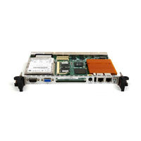
6U CompactPCI Highly Integrated Single Slot Dual Bridge Low Power Pentium-III CPU Module and Rear I/O Transition Module
Brand:
ADLINK Technology
| Category:
Control Unit
| Size: 4 MB
Table of Contents
Table of Contents
6
List of Tables
10
1 Introduction
14
Checklist
14
Front Board
14
Rear Board
15
1.2 Description
16
Table 1-1: Cpci-6760D Model Variations Comparison Table
18
Table 1-2: Cpci-R6760D and Cpci-R6760S Comparison Table
19
1.3 Features
21
1.4 Specifications
22
Specifications of the Front Board (Cpci-6760D Series)
22
Safety Certificate and Test
28
Power Consumption
28
Table 1-3: Power Consumption
28
Specifications of Rear Board Cpci-R6760D
29
Specifications of Rear Board Cpci-R6760S
30
Peripheral Connectivity for Front and Rear Board
33
Table 1-4: Peripheral Connectivity for Cpci-6760D with Cpci
33
Table 1-5: Peripheral Connectivity for Cpci-6760D with Cpci-R6760S
34
1.5 Functional Block Diagram
36
Figure 1-1: Functional Block Diagram
36
1.6 Mechanical Outline Drawing
37
Figure 1-2: Outline Drawing for Cpci-6760D Series Front Board
37
2 Jumpers and Connectors
38
Jumpers and Connectors Map of Cpci-6760D Series Front Board
39
Figure 2-1: Front View
39
Figure 2-2: Bottom and Front Panel View
40
Jumpers and Connectors Map of Cpci-R6760D Board
41
Figure 2-3: Jumpers and Connectors Map of Cpci-R6760D Board
41
Jumpers and Connectors Map of Cpci-R6760S Series Board
42
Figure 2-4: Jumpers and Connectors Map of Cpci-R6760S Series Board
42
Jumpers, Connectors, and LED Indicators on Cpci-6760D
43
JP1 on Cpci-6760D
44
Keyboard and Mouse Combo Connector (CN4) on Cpci-6760D
44
Table 2-1: JP1 Clear CMOS Content
44
Table 2-2: Keyboard/Mouse Combo Connector (CN4) on Cpci-6760D Front Board
44
Ethernet Connectors (CN6, 7)
45
Serial Port COM1 Connector (CN1)
45
Table 2-3: Ethernet Connector LAN1 (CN6) and LAN2 (CN7) on Cpci-6760D Front Board
45
Table 2-4: Serial Port COM1 (CN1) on Cpci-6760D Front Board
45
VGA Connector (CN3)
46
SB (Port A) Connector (CN5)
46
Table 2-5: VGA Connector (CN3) on Cpci-6760D Front Board
46
Table 2-6: USB Connector (CN5) on Cpci-6760D Front Board
46
Connectors (44-Pin, CN2)
47
Table 2-7: Secondary IDE Channel (CN2) on Cpci-6760D Front Board
47
Micro-Switch Connector (CN8)
48
Table 2-8: Micro-Switch Connector CN8 on Cpci-6760D
48
Compactpci J1 Pin Assignments
49
Table 2-9: Compactpci J1 Pin Assignments
49
Compactpci J2 Pin Assignments
50
Table 2-10: Compactpci J2 Pin Assignments
50
Compactpci J3 Pin Assignments
51
Table 2-11: Compactpci J3 Pin Assignments
51
Compactpci J4 Pin Assignments
52
Table 2-12: Comapctpci J4 Pin Assignments
52
Compactpci J5 Pin Assignments
53
Table 2-13: Compactpci J5 Pin Assignments
53
PMC Slot Pin Assignments J11
55
Table 2-14: PMC Slot Pin Assignments J11
55
PMC Slot Pin Assignments J12
56
Table 2-15: PMC Slot Pin Assignments J12
56
LAN Port Indicators (Integrated in LAN1 (CN6) and LAN2 (CN7))
57
Table 2-16: Amber LED Indication in LAN Port
57
IDE Activity LED Indication
58
Table 2-17: Green LED Indication in LAN Port
58
Figure 2-5: IDE Activity LED Indication
58
Power LED Indication
59
WDT LED Indication
59
Self-Hot-Swap LED Indication
59
Table 2-18: IDE Activity LED Indication
59
Table 2-19: Power LED Indication
59
Table 2-20: WDT LED Indication
59
Table 2-21: Self-Hot-Swap LED Indication
59
LAN1, LAN2 Front and Rear I/O Connecting Selection
60
S1, S2: LAN1 Connecting Selection
60
Table 2-22: LAN1 Connecting Selection
60
S3, S4: LAN2 Connecting Selection
61
Table 2-23: LAN2 Connecting Selection
61
Jumpers, Connectors and LED Indicators on the Cpci-R6760D
62
JP2-5 COM2 Mode Selection on Cpci-R6760D Rear Board
63
Table 2-24: JP2-5 COM2 Mode Selection on Cpci-R6760D Rear Board
63
Keyboard Connector (CN13)
64
Mouse Connector (CN12)
64
Ethernet Connectors (CN7, CN8)
64
Table 2-25: Keyboard Connector (CN13) on Cpci-R6760D Rear Board
64
Table 2-26: Mouse Connector (CN12) on Cpci-R6760D Rear Board
64
Table 2-27: Ethernet Connector LAN1 (CN7) and LAN2 (CN8)
64
Serial Port COM2 Connector (CN10)
65
Serial Port COM1 Pin Headers (CN5)
65
Table 2-28: Serial Ports COM2 (CN10) on Cpci-R6760D Rear Board Faceplate
65
Table 2-29: Serial Ports COM1 (CN5) Pin Headers on
65
Parallel Port Connector (CN11)
66
VGA Connector (CN6)
66
Table 2-30: Parallel Ports LPT1 (CN11) on Cpci-R6760D Rear Board Faceplate
66
Table 2-31: VGA Connector (CN6) on Cpci-6760D Front Board
66
USB (Port B) Connector (CN9)
67
IDE Interface (40-Pin, CN2, CN4)
67
Table 2-32: USB Connector (CN9) on Cpci-R6760D Rear Board Faceplate
67
Table 2-33: Primary IDE Channel (CN2) and Secondary IDE Channel (CN4) on Cpci-R6760D Rear Board
67
FDD Interface (34-Pin, CN3)
68
Table 2-34: FDD Interface (CN3) on Cpci-R6760D
68
Compactpci Rj3 Pin Assignments
69
Table 2-35: Compactpci Rj3 Pin Assignments on Cpci-R6760D Rear Board
69
Compactpci Rj5 Pin Assignments (AB Type Connector)
70
Table 2-36: Compactpci J5 Pin Assignments on Cpci-R6760D Rear Board
70
LAN Port Indicators (Integrated in LAN1 (CN7) and LAN2 (CN8))
71
Table 2-37: Amber LED Indication in LAN Port on
71
Table 2-38: Green LED Indication in LAN Port on
71
Jumpers, Connectors and LED Indicators on Cpci-R6760
72
JP2 Cpci-R6760S LAN3 Enable/Disable
73
JP3 Cpci-R6760S LAN4 Enable/Disable
73
Table 2-39: JP2 Cpci-R6760S LAN3 Enable/Disable
73
Table 2-40: JP3 Cpci-R6760S LAN4 Enable/Disable
73
JP4-7 COM2 Mode Selection on Cpci-R6760S Rear Board
74
Table 2-41: JP4-7 COM2 Mode Selection on Cpci-R6760S Rear Board
74
Keyboard Connector (CN22)
75
Mouse Connector (CN21)
75
Table 2-42: Keyboard Connector on Cpci-R6760S Rear Board
75
Table 2-43: Mouse Connector on Cpci-R6760S Rear Board
75
Ethernet Connectors (CN14-17)
76
Serial Port COM2 Connector (CN19)
76
Table 2-44: Ethernet Connector LAN1 to LAN4 on
76
Table 2-45: Serial Ports COM2 (CN19) on Cpci-R6760S Rear Board Faceplate
76
Serial Port COM2 Pin Headers (Reserved, CN13)
77
Serial Port COM1 Pin Headers (Reserved, CN8)
77
Table 2-46: Serial Ports COM2 Pin Headers (CN13) on
77
Table 2-47: Serial Ports COM1 Pin Headers (CN8) on
77
Parallel Port Pin Headers (Reserved, CN1)
78
Table 2-48: Parallel Ports Pin Headers (CN1) on Cpci-R6760S Rear Board
78
VGA Pin Headers (Reserved, CN5)
79
USB (Port B) Connector (CN18)
79
Table 2-49: VGA Pin Headers (CN5) on Cpci-R6760S
79
Table 2-50: USB Connector (CN18) on Cpci-R6760S Rear Board Faceplate
79
IDE Interface (40-Pin, CN2, CN3)
80
Table 2-51: Primary IDE Channel (CN3) and Secondary IDE Channel (CN2) on Cpci-R6760S Rear Board
80
FDD Interface (34-Pin, CN4)
81
Table 2-52: FDD Interface (CN4) on Cpci-R6760S
81
External Ultra-160 SCSI Interface (CN20)
82
Table 2-53: External Ultra-160 SCSI Interface (CN20) on Cpci-R6760S Faceplate
82
Compactpci Rj3 Pin Assignments (Cpci-R6760S)
83
Table 2-54: Compactpci Rj3 Pin Assignments on Cpci-R6760S Rear Board
83
Compactpci Rj4 Pin Assignments (Cpci-R6760S)
84
Table 2-55: Compactpci Rj4 Pin Assignments on Cpci-R6760S Rear Board
84
Compactpci Rj5 Pin Assignments (Cpci-R6760S)
85
Table 2-56: Compactpci Rj5 Pin Assignments on Cpci-R6760S Rear Board
85
LAN Port Indicators (Integrated in LAN1 to LAN4)
86
Table 2-57: Amber LED Indication in LAN Port
86
Table 2-58: Green LED Indication in LAN Port
86
3 Getting Started
88
3.1 CPU Installation
88
3.2 Memory Installation
89
3.3 CF Installation
89
DB-6760CF Outline, Jumper and Connectors
90
Table 3-1: JP1 DB-6760CF Master/Slave Setting
90
Figure 3-1: DB-6760CF Outline
90
DB-6760CF Installation for Cpci-6760D and CF Card Notice
91
Removing DB-6760CF from Cpci-6760D
91
3.4 HDD Installation
92
HDD/FFD Installation for Cpci-6760D
92
Removing HDD/FFD from Cpci-6760D
93
3.5 Device Connection for os Installation
93
Using Cpci-6760D on Adlink's Cbp-6108, 6105, 6515, and 6402 Series Backplane
93
Using Cpci-6760D on Other Backplanes
94
3.6 Notice for Rear I/O Connection
95
The I/O Implementation Is Only Supported by Rear I/O Board
95
The I/O Implementation Is Supported by both Rear I/O and Front I/O
95
LAN1, LAN2 Front and Rear I/O Connecting Selection
96
Table 3-2: LAN1 Connecting Selection
97
Table 3-3: LAN2 Connecting Selection
97
4 Driver Installation
100
4.1 VGA Drivers Installation
101
Driver Installation on Windows 2000
102
Driver Installation on Windows 98
103
Driver Installation on Windows NT
104
4.2 LAN Drivers Installation
105
Software and Drivers Support
105
Driver Installation on Windows 2000
106
Driver Installation on Windows 98
107
Driver Installation on Windows NT
108
4.3 SCSI Drivers Installation
109
Software and Drivers Support
109
Driver Installation on Windows 2000
110
Driver Installation on Windows 98
111
Driver Installation on Windows NT
112
5 Watchdog and Utilities
114
5.1 Watchdog Timer Configuration
114
WDT Programming
114
How to Test the WDT
115
5.2 Hardware Doctor Utility
116
Intel Preboot Execution Environment (PXE)
116
5.4 Intel Adapter Teaming
117
5.5 PICMG 2.1 Hot Swap Support
118
Insertion Process
119
Extraction Process
120
5.6 Self Hot Swap Support
121
BIOS Setting Process
121
Table 5-1: BIOS and os Setting for Self Hot Swap
121
Windows 98 and 2000 Setting Process
122
Insertion Process
123
Extraction Process
124
Warranty Policy
126
Advertisement
Advertisement
Related Products
ADLINK Technology NuIPC cPCI-6760D Series
ADLINK Technology NuIPC cPCI-6760D/P7
ADLINK Technology cPCI-6968
ADLINK Technology cPCI-6969
ADLINK Technology cPCI-6830 Series
ADLINK Technology cPCI-3534
ADLINK Technology cPCI-3544
ADLINK Technology cPCI-8168
ADLINK Technology cPCI-3938
ADLINK Technology cPCI-R6500 Series
ADLINK Technology Categories
Computer Hardware
Motherboard
PCI Card
Control Unit
Desktop
More ADLINK Technology Manuals
Login
Sign In
OR
Sign in with Facebook
Sign in with Google
Upload manual
Upload from disk
Upload from URL