Sign In
Upload
Manuals
Brands
ADLINK Technology Manuals
I/O Systems
DAQe Series
User Manuals: ADLINK Technology DAQe Series Acquisition
Manuals and User Guides for ADLINK Technology DAQe Series Acquisition. We have
1
ADLINK Technology DAQe Series Acquisition manual available for free PDF download: User Manual
ADLINK Technology
DAQe Series
User Manual
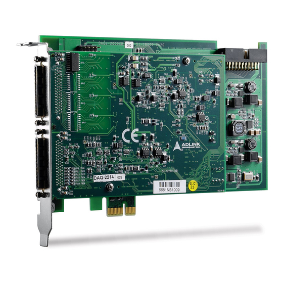
ADLINK Technology DAQe Series User Manual (102 pages)
64-/96-CH High Performance Multi-Function Data Acquisition Card
Brand:
ADLINK Technology
| Category:
I/O Systems
| Size: 1 MB
Table of Contents
Table of Contents
8
List of Tables
10
1 Introduction
14
Features
15
Applications
16
Specifications
16
Table 1-1: Programmabel Input Range
17
Table 1-2: Bandwidth
18
Table 1-3: System Noise
19
Table 1-4: CMRR (DC to 60 Hz)
19
Table 1-5: Settling Time to Full Scale Step
20
Software Support
26
Programming Library
26
DAQ-LVIEW Pnp: Labview Driver
27
D2K-OCX: Activex Controls
27
2 Installation
28
Contents of Package
28
Unpacking
28
Card Layout
30
Daqe-2204/2205/2206/2208
30
Figure 2-1: Daqe-2204/2205/2206/2208 Card Layout
30
Daq-2204/2205/2206/2208
31
Pxi-2204/2205/2206/2208
31
Figure 2-2: DAQ-2204/2205/2206/2208 Card Layout
31
Figure 2-3: PXI-2204/2205/2206/2208 Card Layout
31
PCI Configuration
32
Plug and Play
32
Configuration
32
Troubleshooting
32
3 Signal Connections
34
Connectors Pin Assignment
34
CN1 Connector
35
Table 3-1: CN1 Pin Assignment for DAQ-/Daqe-/PXI-2204/2205/2206
35
Table 3-2: CN1 Pin Assignment for DAQ-/Daqe-/PXI-2208
36
CN2 Connector
37
Table 3-3: CN2 Pin Assignment for DAQ-/Daqe-/PXI-2204/2205/2206
37
Table 3-4: CN2 Pin Assignment Fordaq-/Daqe-/PXI-2208
38
Table 3-5: CN1/CN2 Signal Description
39
SSI Connector
41
Table 3-6: SSI Connector Pin Assignment
41
Table 3-7: SSI Connector Legend
41
Analog Input Signal Connection
42
Types of Signal Sources
42
Input Configurations
42
Figure 3-1: Floating Source and RSE Input Connections
43
Figure 3-2: Ground-Referenced Sources and NRSE Input Connections
43
Differential Input Mode
44
Figure 3-3: Ground-Referenced Source and Differential Input
44
Figure 3-4: Floating Source and Differential Input
44
4 Operation Theory
46
A/D Conversion
46
DAQ-/Daqe-/PXI-2204/2208 AI Data Format
46
Figure 4-1: Synchronous Digital Inputs Block Diagram
47
Figure 4-2: Synchronous Digital Inputs Timing
47
Table 4-1: Bipolar Analog Input Range and Output Digital Code on Daq/Daqe/Pxi-2204/2208
48
Table 4-2: Unipolar Analog Input Range and Output Digital Code on Daq/Daqe/Pxi-2204/2208
48
Daq/Daqe/Pxi-2005/2006/2016 AI Data Format
49
Table 4-3: Bipolar Analog Input Range and Output Digital Code for Daq/Daqe/Pxi-2205/2206
49
Table 4-4: Unipolar Analog Input Range and Output Digital Code for Daq/Daqe/Pxi-2205/2206
49
Software Conversion with Polling Data Transfer
50
Acquisition Mode (Software Polling)
50
Programmable Scan Acquisition Mode
51
Figure 4-3: Scan Timing
52
Specifying Channels, Gains, and Input Configurations in the Channel Gain Queue
53
Trigger Modes
55
Figure 4-4: Pre-Trigger (Trigger Occurs after M Scans)
56
Figure 4-5: Pre-Trigger (Trigger with Scan in Progress)
57
Figure 4-6: Pre-Trigger with M_Enable=0 (Trigger Occurs before M Scans)
58
Figure 4-7: Pre-Trigger with M_Enable=1
59
Figure 4-8: Middle-Trigger with M_Enable = 1
60
Figure 4-9: Middle-Trigger (Trigger Occurs When a Scan Is in Progress)
61
Figure 4-10: Post-Trigger
62
Figure 4-11: Delay Trigger
63
Figure 4-12: Post Trigger with Re-Trigger
64
Bus-Mastering DMA Data Transfer
65
Figure 4-13: Scatter/Gather DMA for Data Transfer
66
D/A Conversion
67
Table 4-5: Bipolar Output Code Table
67
Software Update
68
Table 4-6: Unipolar Output Code Table
68
Timed Waveform Generation
69
Figure 4-14: Typical D/A Timing of Waveform Generation
70
Figure 4-15: Post Trigger Waveform Generation
71
Trigger Modes
71
Figure 4-16: Delay Trigger Waveform Generation
72
Figure 4-17: Re-Triggered Waveform Generation with
72
Figure 4-18: Finite Iterative Waveform Generation with
73
Figure 4-19: Infinite Iterative Waveform Generation with
74
Figure 4-20: Stop Mode I
75
Figure 4-21: Stop Mode II
76
Figure 4-22: Stop Mode III
76
Digital I/O
77
General Purpose Timer/Counter Operation
77
The Basics of Timer/Counter Functions
78
General Purpose Timer/Counter Modes
78
Figure 4-23: Mode1 Operation
79
Figure 4-24: Mode2 Operation
80
Figure 4-25: Mode3 Operation
80
Figure 4-26: Mode4 Operation
81
Figure 4-27: Mode5 Operation
82
Figure 4-28: Mode6 Operation
82
Figure 4-29: Mode7 Operation
83
Figure 4-30: Mode8 Operation
83
Trigger Sources
84
Software-Trigger
84
External Analog Trigger
84
Table 4-7: Analog Trigger SRC1 (EXTATRIG) Ideal Transfer Characteristic
85
Figure 4-31: Analog Trigger Block Diagram
85
Figure 4-32: Below-Low Analog Trigger Condition
86
Figure 4-33: Above-High Analog Trigger Condition
86
Figure 4-34: Inside-Region Analog Trigger Condition
87
Figure 4-35: High-Hysteresis Analog Trigger Condition
88
Figure 4-36: Low-Hysteresis Analog Trigger Condition
88
Figure 4-37: External Digital Trigger
89
User-Controllable Timing Signals
90
Figure 4-38: DAQ Signals Routing
90
DAQ Timing Signals
91
Table 4-8: User-Controllable Timing Signals and
91
Auxiliary Function Inputs (AFI)
93
Table 4-9: Auxiliary Function Input Signals and
93
System Synchronization Interface
95
Table 4-10: SSI Timing Signal and Functions
95
5 Calibration
98
Loading Calibration Constants
98
Auto-Calibration
99
Saving Calibration Constants
99
Warranty Policy
100
Advertisement
Advertisement
Related Products
ADLINK Technology DAQe-2204
ADLINK Technology DAQe-2205
ADLINK Technology DAQe-2206
ADLINK Technology DAQe-2208
ADLINK Technology DAQ Series
ADLINK Technology DAQ-2206
ADLINK Technology DAQ/PXI-2500 Series
ADLINK Technology DAQ/PXI-2501
ADLINK Technology DAQ/PXI-2502
ADLINK Technology DAQ-2501
ADLINK Technology Categories
Computer Hardware
Motherboard
PCI Card
Control Unit
Desktop
More ADLINK Technology Manuals
Login
Sign In
OR
Sign in with Facebook
Sign in with Google
Upload manual
Upload from disk
Upload from URL