JVC KD-LX30R Service Manual
Cd receiver
Hide thumbs
Also See for KD-LX30R:
- Service manual (9 pages) ,
- Installation & connection manual (4 pages) ,
- Service manual (74 pages)
Table of Contents
Advertisement
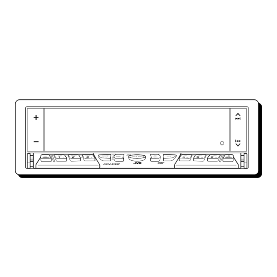
KD-LX30R/KD-LX10R
VICTOR COMPANY OF JAPAN, LIMITED
MOBILE ELECTRONICS DIVISION,10-1,1Chome,Ohwatari-machi,Maebashi-city,Japan
(No.49551)
SERVICE MANUAL
Contents
Preventing static electricity
Instructions
Printed in Japan
200003(O)
CD RECEIVER
KD-LX30R
KD-LX10R
S C M
M O N O
L O C A L
MODE
A TT
TP
I N T
R P T
R N D
S E L
7
8
9
BAND
S
DISP
SOURCE
RDS
PTY
10
11
12
O F F
M
S
KD-LX30R
Remote
Line IN Sub Woofer
controller
KD-LX30R
KD-LX10R
Functions of the mechanism under
1-2
the servise mode
1-3
Flow of functional until TOC read
1-4~22
2-1
2-13
2-14
2-14
2-15
This service manual is made from 100% recycled paper.
COPYRIGHT
2000 VICTOR COMPANY OF JAPAN, LTD.
KD-LX30R/KD-LX10R
E ---- Continental Europe
2-18
2-20
2-22
2-41
2-43
2-47,48
3-1~17
No.49551
Mar. 2000
Advertisement
Chapters
Table of Contents

Related Manuals for JVC KD-LX30R


Summary of Contents for JVC KD-LX30R
-
Page 1: Table Of Contents
KD-LX30R/KD-LX10R KD-LX30R/KD-LX10R SERVICE MANUAL CD RECEIVER KD-LX30R KD-LX10R Area Suffix E ---- Continental Europe S C M M O N O L O C A L MODE A TT I N T R P T R N D S E L... - Page 2 Preventing static electricity 1.Grounding to prevent damage by static electricity Electrostatic discharge (ESD), which occurs when static electricity stored in the body, fabric, etc. is discharged, can destroy the laser diode in the traverse unit (optical pickup). Take care to prevent this when performing repairs. 2.About the earth processing for the destruction prevention by static electricity Static electricity in the work area can destroy the optical pickup (laser diode) in devices such as CD players.
-
Page 3: Safety Precaution
Safety precaution ! CAUTION Burrs formed during molding may be left over on some parts of the chassis. Therefore, pay attention to such burrs in the case of preforming repair of this system. ! CAUTION Please use enough caution not to see the beam directly or touch it in case of an adjustment or operation check. -
Page 4: Disassembly Method
Disassembly method Bottom cover Removing the top chassis (See Fig.1 to 5) Remove the two screws A attaching the bottom cover to the top chassis on the bottom of the body. Remove the two screws B attaching the top chassis on both sides of the body. - Page 5 Removing the main board assembly (See Fig.6 and 7) Prior to performing the following procedure, remove the top chassis. Disconnect the flexible harness from connector CN504 CN701, the card wire from CN702 on the main board CN503 harness from CN503 CN504 CN701 respectively.
- Page 6 Removing the front panel assembly (See Fig.6,8 and 9) Prior to performing the following procedure, remove CN504 the top chassis assembly. CN503 CN701 Disconnect the flexible harness from connector CN701 on the main board assembly. Remove the four screws N attaching the front panel assembly on both sides of the body.
- Page 7 Removing the lifter unit (See Fig.11) Prior to performing the following procedure, remove the top chassis assembly and the front panel assembly. Disconnect the harness from connector CN503and CN504 CN503 CN504 on the main board. Remove the four screws P and detach the lifter unit from the bottom cover.
- Page 8 Removing the operation assembly (See Fig.14 to 17) Prior to performing the following procedure, remove the top chassis assembly, the front panel assembly and the lifer unit. Bracket (R) Remove the screws S attaching the right and left Bracket (L) brackets which fix gears on both sides of the operation assembly.
- Page 9 Removing the operation switch board (See Fig.18 and 19) Prior to performing the following procedure, remove the operation assembly. Remove the six screws T attaching the button panel on the operation assembly. Pull out the operation switch board from inside of the button panel.
- Page 10 Removing the CD mechanism control Damper bracket board (See Fig.1 and 2) Pickup cover Remove the screw N and the pickup cover attached to the front bracket with the two double-sided tapes. Unsolder the part f and g on the CD mechanism control board.
- Page 11 Loading motor Belt Fig.5 Removing the CD mechanism ass’y CD mechanism ass’y (See Fig.1, 6 to 9) Damper bracket Prior to performing the following procedure, remove the CD mechanism control board and the front bracket (loading motor). Flame Remove the three screws I and the damper bracket. Raise the both sides fix arms and move the fix plates Fig.6 in the direction of the arrow to place the four shafts l...
-
Page 12: See Fig
Removing the feed motor ass’y Part n FD screw (See Fig.10) Feed motor ass’y Prior to performing the following procedure, remove the CD mechanism control board, the front bracket Part O (loading motor) and the CD mechanism ass’y. Remove the two screws K and the feed motor ass’y. Pickup unit FD gear Pickup unit... - Page 13 Damper bracket Removing the CD mechanism control CD mechanism ass’y board(See Fig.1 and 2) Unsolder the part a and b on the CD mechanism control board. Remove the stator c fixing the CD mechanism control board and the damper bracket (To remove the stator smoothly, pick up the center part).
- Page 14 Removing the loading motor Loading motor (See Fig.3 to 5) Prior to performing the following procedure, remove the CD mechanism control board. Belt Remove the two springs f attaching the CD mechanism ass’y and the front bracket. Fig.5 Remove the two screws B and the front bracket while pulling the flame outward.
- Page 15 Removing the feed motor ass’y Part j FD screw (See Fig.10) Feed motor ass’y Prior to performing the following procedure, remove the CD mechanism control board, the front bracket Part k (loading motor) and the CD mechanism ass’y. Remove the two screws F and the feed motor ass’y. Pickup unit FD gear Pickup unit...
-
Page 16: Adjustment Method
Adjustment method Caution : Replacing the pickup To prevent damage to the laser diode Caution : static electricity destroys the laser diode. Solder rejection or cuts a pattern with nipper at shortstop point after short Always take countermeasure performing repairs around the laser circuiting with clip with terminal face of pickup. -
Page 17: Maintenance Of Laser Pickup
Maintenance of laser pickup (1) Cleaning the pick up lens Before you replace the pick up, please try to clean the lens with a alcohol soaked cotton swab. (2) Life of the laser diode When the life of the laser diode has expired, the following symptoms will appear. -
Page 18: Extention Cord Connecting Method
Extension cord connecting method Using the extention cords to connect the front panel with the main board Remove the main board follwing the disassembly methode. Then reattachi the heat sink to main board. Using the 2pin extention cord (EXTLX001-2p), Using the jig board (EXTLX002-SWPWB), its connect the harness of the feed motor (L) assembly installing to the chassis, then using 4pin extention with the connector CN503 on the main board. - Page 19 Extension cord list for KD-LX10/KD-LX30 EXTLX002-JIG : Kit including the following 8 extension parts. Parts number Quantity Description EXTLX001-2P 2Pin, 30cm extension cord EXTLX001-6PF 6Pin, 30cm flat wire EXTLX001-6PC 6Pin x 2, interlocking connector EXTLX002-16PF 16Pin flat wire EXTLX002-16PC 16Pin, interlocking connector EXTLX002-SWPWB 3 switch PWB EXTLX002-4P...
- Page 20 Reassembly 1. Perform reassembly be reversing the removing process of "removal of main parts". CAUTION 1: Prior to reattaching the heat sink, make sure to reattache the top chassis.
- Page 21 Functions of the mechanism under the service mode With the three error modes stored in maximum in the internal memory of the mechanism in the body of this system, it is posible under the service mode to call the contents of error according to the following steps when any error has occurred.
- Page 22 1. Display of mechanism error Occurrence condition Description Error codes 09 0011 1. SW4 is not turned off. Disc loading error 09 0013 2. SW3 is not turned on. Eject error 01 0021 1. SW# is not turned off. 1. In case SW2 has been positioned to "L" before 80 0031 Error during standby for loading starting loading during waiting for 15sec.
- Page 23 Flow of functional operation until TOC read Power ON • When the laser diode correctly Set Function to CD • When the pickup correctly moves emits to the inner area of the disc Microprocessor Microprocessor Disc inserted commands commands MN662748RPM 57 MN662748RPM "32"...
- Page 24 Feed Section Is the voltage output at Is the wiring for IC941 Is 5V present at IC601 Check CD 9V IC631 pin "26" 2.5V or (10) ~ (15) correct? pin "5"? and 5V. Check the vicinity of IC941. Is 4V present at both Is 6V or 2V present at Check the feed motor sides of the feed motor?
- Page 25 BA3220FV-X (IC301,IC401) : Driver 1. Pin layout & Block diagram LGND OUTL OUTR RGND CR - CR + REFL REFR FILTER 2. Pin functions Symbol Function Power supply terminal for amp. power supply terminal. input terminal. Negative feedback terminal. Filter terminal. Negative feedback terminal.
- Page 26 BA4905-V3 (IC961) : Regulator 1.Terminal layout 2.Block diagram REGULATOR RESET RESET COMP VDD 5.7V CD 8V AUDIO 9V CTRL ILM 10V 3.Pin function Pin no. Symbol Function RESET If VDD voltage becomes 4V or less.RESET output becomes low level. EXT output This output voltage is approximately 0.5V lower than VCC.
- Page 27 BD3860K (IC911) : E. volume 1. Pin layout 2. Block diagram GND FIL VCC SEL1 VIN1 LOUD1 HF1 LF1 DET1 VCA1 MIX1 BBOUT1 TIN1 TNF1 BNF1 BOUT1 POWER FADER SUPPLY MAIN INPUT CH1 FRONT OUTF1 TREBLE BASS VOLUME GAIN 0 to -5 dB LOW(f=50Hz) 6dB 0 to -40 dB -14 to +14dB...
- Page 28 BR24C32F-X (IC703) : EEPROM 1. Pin layout 2. Pin function Symbol Function Slave address set Slave address set Slave address set Gorund (V) Slave and word address Serial data input, Serial data output Serial clock input Write protect Power supply 3.
- Page 29 BU4066BCFV-X (IC322) : Quad analog switch 1. Pin layout & Block diagram I/O4 O/I4 O/I3 I/O3 I/O1 O/I1 O/I2 I/O2...
-
Page 30: Description Of Major Ics
Description of major ICs FAN8037 (IC581) : CD driver 1. Pin layout & Block diagram 48 47 46 45 44 43 42 41 40 39 38 37 STAND BY T.S.D ALL MUTE POWER SAVE 13 14 15 16 17 18 19 20 21 22 23 24 2. - Page 31 HD74HC126FP-X (IC771) : Buffer 1. Pin layout 2. Function Inputs Outputs 3. Block diagram Output Input Output Sample as Load Circuit 1 Output Sample as Load Circuit 1 Output Sample as Load Circuit 1...
- Page 32 IC-PST600M/G/-W (IC702) : System reset Vout...
- Page 33 LA3460M-X (IC31) : FM noise canceller & Stereo MPX demodulator 1. Pin layout 2. Block diagram DRIVER VCO STOP PACAN SCHMIT SEPARATION ADJ. ANTI-BRIDGE MAIN GATE DECODER TRIG CONTROL 3. Pin function Function Description Noise sense Noise sensitivity adjustment Noise AGC Gate time Signal hold Pilot output...
- Page 34 LA4743B (IC941) :Power amp 1.Terminal layout 2 3 4 5 6 7 8 9 10 11 12 13 14 15 16 17 18 19 20 21 22 23 24 25 2.Block diagram 3.Pin function No. Symbol Function No. Symbol Function Header of IC LFIN Front Lch input...
- Page 35 LC75811W (IC602) : LCD driver 1. Pin layout 2. Block diagram COMMON SEGMENT DRIVER DRIVER LATCH CGRAM CGROM ADRAM VLCD INSTRUCTION 5x9x16 5x9x240 DECODER bits bits bits VLCD1 VLCD2 ADDRESS DCRAM INSTRUCTION VLCD3 COUNTER 48x8 REGISTER bits ADDRESS REGISTER TIMING GENERATOR SHIFT REGISTER CLOCK...
- Page 36 LC75823W (IC601,IC602) : LCD Driver 1. Pin Layout & Symbol 64 63 62 61 60 59 58 57 56 55 54 53 52 51 50 49 17 18 19 20 21 22 23 24 25 26 27 28 29 30 31 32 2.
- Page 37 NJM2100M-W (IC821) : Dual operation amplifier 1. Pin layout A OUTPUT A - INPUT B OUTPUT A + INPUT B - INPUT B + INPUT 2. Block diagram - INPUT OUTPUT + INPUT...
- Page 38 NJM2904M-W (IC951) : Dual operation amplifier 1. Pin layout A OUT A - IN B OUT A + IN B - IN B + IN 2. Block diagram INPUTS OUTPUT...
- Page 39 NJM4565M-WE (IC361,IC461) : Ope. amp A OUTPUT A INPUT B OUTPUT A INPUT B INPUT B INPUT...
- Page 40 NJM4565M-W (IC151,IC171,IC323) : Ope amp. A OUTPUT A -INPUT B OUTPUT A +INPUT B -INPUT B +INPUT...
- Page 41 RPM6938-SV4 (IC603) : Remote control receiver Comp Rout Detector conversion trimming circuit magnetic shield...
- Page 42 SAA6579T-X (IC51) : RDS demodulator 1. Pin layout 2. Pin function Symbol Function QUAL Quality indication output RDDA RDS data output Vref Reference voltage output (0.5VDDA) Multiplex signal input VDDA +5V supply voltage for analog part VSSA Ground for analog part (0V) Sub carrier input to comparator SCOUT Sub carrier output of reconstruction filter...
- Page 43 TA2109F-X (IC501) : RF amp. 1. Pin layout 2. Block diagram 15k ohm 30k ohm 7.67k ohm 15k ohm 10k ohm SBAD 10k ohm 20uA 50k ohm 30k ohm 20pF 10k ohm 10k ohm 36pF 21k ohm 29k ohm 2VRO 7.96k ohm 10k ohm 24k ohm 24k ohm...
- Page 44 TC9462F (IC521) : DSP & DAC 1.Pin Layout 2.Pin Function (1/2) Symbol Pin No. Function Test mode terminal. Normally, keep at open TEST0 Playback speed mode flag output terminal Playback speed mode flag output terminal UHSO Sub code Q data emphasis flag output terminal. "H"=ON "L"=OFF EMPH Channel clock output terminal.(44.1kHz) "H"=Rch "L"=Lch LRCK...
- Page 45 2.Pin Function (2/2) Symbol Pin No. Function RFRP signal center level input terminal RFCT RFRP zero cross input terminal RFZI RF ripple signal input terminal RFRP Focus error signal input terminal Sub-beam adder signal input terminal SBAD Test input terminal Normally, keep at "vref" level TSIN Tracking error signal input terminal.
- Page 46 UPD784215GC-167 (IC701) : CPU 1. Pin layout 2. Pin function (1/2) Symbol Function CD mechanism detect switch CD mechanism detect switch CD mechanism detect switch REST-SW Reset signal input terminal from CD mechanism Loading motor control signal input terminal Loading motor control signal input terminal DIMMER-OUT DIMMER signal output terminal LCD-PWR...
- Page 47 Chip enable 2 output terminal for LCD driver Motor speed control signal output terminal Tray motor control signal output terminal STAGE1 Initial setting H:KD-LX30R L:KD-LX10R BUCK Micro computer interface clock signal output terminal Chip enable signal output terminal for micro computer interface...
-
Page 48: Block Diagrams
PLLDA LEVEL FRONTL,FRONTR FRONT PLLCL VOL-DA Line out RDSDA VOL-CLK REARL,REARR REAR RDSSCK AMAF IC703 IC771 IC821 CH-L EPROM JVC BUS CRUISE CH-R IC701 SI/SO,SO,I/OBUSINT,BUSSCK CRUISE CDON AU.L,AU.R CASW1 RESET LCDDA IC151 CASW2 AU.LI,AU.RI IC171 W.VOL Line IN IC321 RESET... - Page 49 PLLCE REAR L PLLDA LEVEL PLLCL VOL-DA Line out REAR R RDSDA VOL-CLK RDSSCK AMAF IC703 IC771 IC821 CH-L EPROM JVC BUS CRUISE CH-R IC701 SI/SO,SO,I/OBUSINT,BUSSCK CRUISE CDON CASW1 RESET LCDDA IC151 CASW2 RESET IC702 LCDCL CD LPF CASW3 REMOCON...
-
Page 50: Standard Schematic Diagrams
Standard schematic diagrams KD-LX30R Tuner & Main section TUNER SIGNAL CD SIGNAL CD CHANGER SIGNAL AUX SIGNAL FRONT SIGNAL RIGHT SIGNAL Parts are safety assurance parts. When replacing those parts make sure to use the specified one. - Page 51 KD-LX30R CD & LCD section CD SIGNAL...
- Page 52 KD-LX10R Tuner & Main section TUNER SIGNAL CD SIGNAL CD CHANGER SIGNAL FRONT SIGNAL REAR SIGNAL Parts are safety assurance parts. When replacing those parts make sure to use the specified one.
- Page 53 KD-LX10R CD & LCD section CD SIGNAL...
-
Page 54: Printed Circuit Board
Printed circuit boards KD-LX30R Main board (Forward side) Main board (Reverse side) LCD board (Forward side) LCD board (Reverse side) Switch board (Forward side) Switch board (Reverse side) - Page 55 KD-LX10R Main board (Forward side) Main board (Reverse side) LCD board (Forward side) LCD board (Reverse side) Switch board (Forward side) Switch board (Reverse side)
-
Page 56: Parts List
PARTS LIST [ KD-LX30R ] [ KD-LX10R ] * All printed circuit boards and its assemblies are not available as service parts. Area suffix E ----------- Continental Europe - Contents - Exploded view of general assembly and parts list CD mechanism assembly and parts list... -
Page 57: Exploded View Of General Assembly And Parts List
Exploded view of general assembly and parts list Block No. KD-LX10R 39 55... - Page 58 Parts list (General assembly) Block No. M1MM Parts number Parts name Q'ty Description Item Area --------------- CD MECHA LV41606-001A FFC P.MECHA LV10189-001A-N CHASSIS TOP LV10188-003A FRONT COVER LV40828-002A BLIND LV31602-001A SIDE HEAT SINK LV31603-001A INSULATOR QYSPST2004M SCREW QYSDST2604Z SCREW 3 T. CHAS+CD MECH QYSDSF2610Z TAPPING SCREW 1 T.
- Page 59 6 FOR GEAR 1-6 WDM214540 WASHER 2 FOR CLUTCH ASS' QYSPSPU1725M SCREW 4 LO.UNIT A+DIS.P LV30981-005A CLUTCH ASS'Y LV10317-005A BUTTON PANEL 1 KD-LX30R LV10317-004A BUTTON PANEL 1 KD-LX10R LV10318-001A BUTTON BASE LV20615-002A PRESET BUTTON 1 LV20616-002A PRESET BUTTON 2 LV31613-001A...
- Page 60 Block No. M1MM Parts number Parts name Q'ty Description Item Area LV41752-001A POEWR IC BKT LV40792-001A REG.IC BRACKET QMFZ039-150-T FUSE QAM0105-002 CAR CABLE LV40846-005A SPACER(F) LV40848-009A SPACER(P) LV40848-009A SPACER(P) LCD 1 QLD0111-001 LCD MODULE 1 KD-LX10R QLD0110-001 LCD MODULE 1 KD-LX30R...
-
Page 61: Cd Mechanism Assembly And Parts List
CD mechanism assembly and parts list Block No. Grease G-31SA TN-CCD1001Z-138 G-31SA(Bottom side) RX-405 106 29... - Page 62 Parts list (CD mechanism) Block No. M2MM Parts number Parts name Q'ty Description Item Area 30310101T FRAME 30310103T DANPER PIN 30310107T UPPER PLATE 30310108T SEL STOP PLATE 30310142T SEL ARM (L)L 30310143T SEL ARM (R)L 30310145T S ARM SPRING(L) 30310112T TRIG LEVER 30310155T TRIG PL(Z)
- Page 63 Parts list (CD mechanism) Block No. M2MM Parts number Parts name Q'ty Description Item Area 19501403T WIRE CLAMPER 30311037T PICK UP FPC(Z) 30311036T CONNECT.PCB(Z-J 30311038T WIRE (5P-Z) 30311039T WIRE (LD-Z) 30311040T WIRE (FD-Z) 30311041T WIRE (RS-Z) 64180402T DET SWITCH 2 ESE22MH1 64180403T DET SWITCH 2 ESE22MH3...
-
Page 64: Electrical Parts List
C 22 NCB21HK-103X C CAPACITOR C 253 NCS21HJ-121X C CAPACITOR C 23 NCB21HK-472X C CAPACITOR C 272 QEK41CM-106 E CAPACITOR KD-LX30R C 24 NCB21EK-104X C CAPACITOR C 273 QERF0JM-226Z E CAPACITOR KD-LX30R C 25 QERF1HM-474Z E CAPACITOR .47MF 20% 50V... - Page 65 KD-LX10R C 791 QERF1HM-104Z E CAPACITOR .10MF 20% 50V C 464 NCS21HJ-101X CER.CAPACITOR-M KD-LX10R C 821 NCB21HK-183X C CAPACITOR KD-LX30R C 467 QEKJ0JM-476Z AL E.CAPACITOR KD-LX10R C 822 NCB21EK-393X C CAPACITOR KD-LX30R C 501 QERF0JM-107Z E CAPACITOR 100MF 20% 6.3V...
- Page 66 Parts name Remarks Area Item Parts number Parts name Remarks Area D 11 MA152WK-X SI DIODE Q 131 2SD1048/6-7/-X TRANSISTOR KD-LX30R D 31 1SS355-X DIODE Q 132 2SD1048/6-7/-X TRANSISTOR D 101 MA152WK-X SI DIODE Q 161 2SD601A/R/-X TRANSISTOR D 111...
- Page 67 Remarks Area Item Parts number Parts name Remarks Area R 134 NRSA02J-681X MG RESISTOR R 331 NRSA02J-104X MG RESISTOR KD-LX30R R 135 NRSA02J-101X MG RESISTOR KD-LX30R R 332 NRSA02J-104X MG RESISTOR KD-LX30R R 136 NRSA02J-101X MG RESISTOR R 333 NRSA02J-473X...
- Page 68 R 523 NRSA02J-472X MG RESISTOR R 739 NRSA02J-473X MG RESISTOR R 524 NRSA02J-472X MG RESISTOR R 740 NRSA02J-473X MG RESISTOR KD-LX30R R 525 NRSA02J-103X MG RESISTOR R 741 NRSA02J-473X MG RESISTOR KD-LX10R R 531 NRSA02J-103X MG RESISTOR R 742 NRSA02J-103X...
- Page 69 NRSA02J-473X MG RESISTOR S 651 NSW0120-002X PUSH SWITCH S 652 NSW0120-002X PUSH SWITCH S 653 NSW0120-002X PUSH SWITCH TH951 NAD0021-103X THERMISTOR KD-LX30R TH981 NAD0021-103X THERMISTOR TU 1 QAU0157-001 TUNER PACK VR 31 QVP0004-503Z SEMI.V.RESISTOR X 51 QAX0263-001Z CRYSTAL X 521...
- Page 70 R 640 NRSA02J-272X MG RESISTOR C 607 NCB21HK-104X C CAPACITOR R 641 NRSA02J-392X MG RESISTOR C 608 NCB21HK-104X C CAPACITOR KD-LX30R R 642 NRSA02J-821X MG RESISTOR C 608 NCB21HK-102X C CAPACITOR KD-LX10R R 643 NRSA02J-821X MG RESISTOR C 609 NDC21HJ-101X...
-
Page 71: Packing Materials And Accessories Parts List
Packing materials and accessories parts list Block No. Block No. A1,A4,A7 KD-LX30R ONLY KIT1:A9~A13 A2,A3,A5,A6 Front view... -
Page 72: 1 Kd-Lx10R
A 11 VKZ4328-001 LOCK NUT A 12 WNS5000Z WASHER A 13 FSKL4010-002 HOOK A 14 RM-RK31 REMOCON 1 KD-LX30R ONLY A 15 --------------- BATTERY 1 KD-LX30R ONLY A 16 FSKM2004-202 MOUNTING SLEEVE A 17 LV10187-001A-N TRIM PLATE A 18 QAM0106-001...
Need help?
Do you have a question about the KD-LX30R and is the answer not in the manual?
Questions and answers