Table of Contents
Advertisement
SERVICE MANUAL
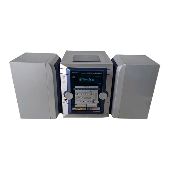
COMPACT DISC STEREO SYSTEM
SYSTEM
NSX–VC38
• This Service Manual is the "Revision Publishing" and replaces "Simple Manual"
NSX-VC38 <HR> (S/M Code No. 09-004-430-3T1).
• If requiring information about the CD mechanism, see Service Manual of AZG-1,
(S/M Code No. 09-001-335-3NG).
NSX-VC38
BASIC TAPE MECHANISM : 6ZM-3 PR2NM
BASIC CD MECHANISM : AZG-1 VZD3RDM
CD
CASSEIVER
CX–NVC38
S/M Code No. 09-006-430-3R1
REMOTE
SPEAKER
CONTROLLER
SX–NBL25
RC–ZAS07
HR, HS
Advertisement
Table of Contents

Subscribe to Our Youtube Channel
Related Manuals for Aiwa NSX-VC38


Summary of Contents for Aiwa NSX-VC38
- Page 1 SX–NBL25 RC–ZAS07 • This Service Manual is the "Revision Publishing" and replaces "Simple Manual" NSX-VC38 <HR> (S/M Code No. 09-004-430-3T1). • If requiring information about the CD mechanism, see Service Manual of AZG-1, (S/M Code No. 09-001-335-3NG). S/M Code No. 09-006-430-3R1...
-
Page 2: Specifications
SPECIFICATIONS Main unit CX-NVC38 <Compact disc player section> Laser Semiconductor laser (λ =780 nm) <FM Tuner section> D/A converter 1 bit dual Tuning range 87.5 MHz to 108 MHz Signal-to-noise ratio 85 dB (1 kHz, 0 dB) Usable sensitivity (IHF) 13.2 dBf Harmonic distortion 0.05 % (1 kHz, 0 dB) -
Page 3: Protection Of Eyes From Laser Beam During Servicing
PROTECTION OF EYES FROM LASER BEAM DURING SERVICING CAUTION This set employs laser. Therefore, be sure to follow carefully the instructions below when servicing. Use of controls or adjustments or performance of proce- dures other than those specified herin may result in WARNING!! hazardous radiation exposure. -
Page 4: Note On Before Starting Repair
NOTE ON BEFORE STARTING REPAIR 1. Forced discharge of electrolytic capacitor of power supply block When repair is going to be attempted in the set that uses relay circuit in the power supply block, electric potential is kept charged across the electrolytic capacitors (C101, 102) even though AC power cord is removed. - Page 5 In such a case, check also if the POWER AMPLIFIER circuit or power supply circuit has any abnormalities or not. 2-2. Regarding reset There are cases that the machine does not work correctly because the MICROCOMPUTER is not reset even though the AC power cord is re-inserted, or the software reset (pressing the STOP key + POWER key) is performed.
-
Page 6: Electrical Main Parts List
ELECTRICAL MAIN PARTS LIST REF. NO. PART NO. KANRI DESCRIPTION REF. NO. PART NO. KANRI DESCRIPTION 87-010-197-080 CAP,CHIP 0.01 DM 87-010-403-080 CAP,ELECT 3.3-50V 87-020-454-010 IC,DN6851 C115 87-010-404-080 CAP,E 4.7-50 M 11L SME 87-A21-398-010 IC,STK490-110 C116 87-010-404-080 CAP,E 4.7-50 M 11L SME 87-A20-783-040 C-IC,BA7762AFS C151... - Page 7 REF. NO. PART NO. KANRI DESCRIPTION REF. NO. PART NO. KANRI DESCRIPTION C508 87-016-669-080 C-CAP,S 0.1-25 K B C793 87-010-404-080 CAP,ELECT 4.7-50V C509 87-016-669-080 C-CAP,S 0.1-25 K B C795 87-010-197-080 CAP,CHIP 0.01 DM C510 87-010-184-080 CHIP CAPACITOR,3300P(K) C796 87-010-197-080 CAP,CHIP 0.01 DM C511 87-010-177-080 C-CAP,S 820P-50 SL...
- Page 8 REF. NO. PART NO. KANRI DESCRIPTION REF. NO. PART NO. KANRI DESCRIPTION C995 87-010-178-080 CHIP CAP,1000P C361 87-010-178-080 CHIP CAP,1000P C997 87-010-196-080 CHIP CAPACITOR,0.1-25 C362 87-010-178-080 CHIP CAP,1000P C998 87-010-260-080 CAP,ELECT 47-25V C371 87-010-178-080 CHIP CAP,1000P C999 87-A11-155-080 CAP,TC U 0.01-16 Z F C372 87-010-178-080 CHIP CAP,1000P...
-
Page 9: Chip Resistor Part Code
REF. NO. PART NO. KANRI DESCRIPTION S323 87-A90-164-080 SW,TACT SKNQAB(N) CN101 87-A61-011-010 CONN,13P H BLK TAC-L13P-A3 S324 87-A90-164-080 SW,TACT SKNQAB(N) CN102 87-A61-011-010 CONN,13P H BLK TAC-L13P-A3 S325 87-A90-164-080 SW,TACT SKNQAB(N) CNA101 8A-NF8-656-010 CONN ASSY,5P TID-A 400 S326 87-A90-164-080 SW,TACT SKNQAB(N) R129 87-A00-669-080 RES,M/F 0.22-2W J RA... -
Page 10: Transistor Illustration
TRANSISTOR ILLUSTRATION E C B E C B B C E CD1585 DTC114ES 2SB1370 CSA952 KTC3199 CSC4115 KTA1266 KTC3198 2SK360 2SK2158 2SA1235 CSD1306 2SC2714 KRA104S 2SC3052 KRC102S CMBT5401 RT1P141C CMBT5551 RT1P144C – 10 –... -
Page 11: Pin Connection
FL (HNA–10SS12) GRID ASSIGNMENT / ANODE CONNECTION / PIN CONNECTION GRID ASSIGNMENT ANODE CONNECTION PIN CONNECTION – 11 –... -
Page 12: Wiring - 1 (Main)
WIRING – 1 (MAIN) <HR> – 12 –... -
Page 13: Wiring - 2 (Main)
WIRING – 2 (MAIN) <HS> – 13 –... - Page 14 SCHEMATIC DIAGRAM – 1 (MAIN : 1 / 3) – 14 –...
- Page 15 SCHEMATIC DIAGRAM – 2 (MAIN : 2 / 3 <DECK SECTION> / HEAD – 1) – 15 –...
- Page 16 SCHEMATIC DIAGRAM – 3 (MAIN : 3 / 3 <TUNER SECTION>) <HR> – 16 –...
- Page 17 SCHEMATIC DIAGRAM – 4 (MAIN : 3 / 3 <TUNER SECTION>) <HS> – 17 –...
-
Page 18: Wiring - 3 (Front)
WIRING – 3 (FRONT) – 18 –... -
Page 19: Schematic Diagram - 5 (Front / Deck)
SCHEMATIC DIAGRAM – 5 (FRONT / DECK) – 19 –... - Page 20 WIRING – 4 (AMP 1F) – 20 –...
- Page 21 SCHEMATIC DIAGRAM – 6 (AMP 1F) – 21 –...
- Page 22 WIRING – 5 (PT) – 22 –...
-
Page 23: Schematic Diagram - 7 (Pt)
SCHEMATIC DIAGRAM – 7 (PT) – 23 –... - Page 24 WIRING – 6 (DECK / HEAD – 1) – 24 –...
-
Page 25: Ic Block Diagram
IC BLOCK DIAGRAM – 25 –... - Page 26 – 26 –...
- Page 27 IC DESCRIPTION µ PD780226GF-017-3BA Pin No. Pin Name Description O-MOTOR DECK MOTOR ON/OFF output. O-SOL1 DECK1 solenoid output. O-SOL2 DECK2 solenoid output. – Not connected. O-REV_LED PRESET (REV) LED ON/OFF output. O-SET_LED SET LED ON/OFF output. O-CLEAR_LED CLEAR LED ON/OFF output. O-FWD_LED PRESET (FWD) LED ON/OFF output.
- Page 28 Pin No. Pin Name Description I-CDSW CD mecha switch input. I-SPEANA_L A/D L-input for spectrum analyser level display. I-SPEANA_R A/D R-input for spectrum analyser level display. 46 ~ 48 I-KEY1 ~ I-KEY3 Key1 ~ Key3 input. I-TU_SIG Tuner signal input. AVSS –...
- Page 29 IC, LC72131D Pin No. Pin Name Description X-IN A crystal oscillator (4.5MHz) is connected between these pins. X-OUT – Not connected. To enable the IC. Active "H". Digital data input from CPU (µPD780226GF-017-3BA) when relevant key is operated. Active "H". To clock in the data DI.
- Page 30 ADJUSTMENT <TUNER / DECK / FRONT> < TUNER SECTION > 1. Clock frequency Check 11. DC Balance / Mono Distortion Adjustment Settings : • Test point : TP2 (CLK) Settings : • Test point : TP3, TP4 (DC) Method : Set to AM(MW) 1602kHz and check that the test •...
- Page 31 18. REC/PB Frequency Response Adjustment (DECK 2) Settings : • Test tape : TTA–602 • Test point : TP8 (Lch), TP9 (Rch) • Input signal : 1kHz / 8kHz (–20VU / –26dBV) • Adjustment location : SFR451 (Lch) SFR452 (Rch) Method : Apply a 1kHz signal and REC mode.
-
Page 32: Cd Test Mode
CD TEST MODE – 32 –... -
Page 33: Mechanical Exploded View
MECHANICAL EXPLODED VIEW 1 / 1 <HR> AZG-1 VZD3RDM P.C.B HT-SINK P.C.B FL901 HT-SINK P.C.B P.C.B PLATE,EARTH MIC CHAS,MAIN 6ZM-3 PR2NM PLATE,EARTH MECHA – 33 –... -
Page 34: Mechanical Parts List
MECHANICAL PARTS LIST 1 / 1 <HR> REF. NO. PART NO. KANRI DESCRIPTION REF. NO. PART NO. KANRI DESCRIPTION 1 8A-NF0-007-010 WINDOW,CASS 2 31 8A-NF8-005-010 PANEL,TOP 2 8A-NF0-006-010 WINDOW,CASS 1 32 8A-NF8-006-010 WINDOW,TOP 3 8A-NF0-004-010 BOX,CASS 2 33 8A-NF8-206-010 HLDR,PWB M 4 8A-NF0-045-010 BOX,CASS 1 D 34 84-ZG1-245-210... - Page 35 MECHANICAL EXPLODED VIEW 1 / 1 <HS> AZG-1 VZD3RDM P.C.B HT-SINK P.C.B FL901 HT-SINK VM P.C.B P.C.B PLATE,SHLD BINDER,WIRE PLATE,EARTH MIC CHAS,MAIN 6ZM-3 PR2NM PLATE,EARTH MECHA – 35 –...
- Page 36 MECHANICAL PARTS LIST 1 / 1 <HS> REF. NO. PART NO. KANRI DESCRIPTION REF. NO. PART NO. KANRI DESCRIPTION 1 8A-NF0-007-010 WINDOW,CASS 2 31 82-NF7-210-110 GUIDE,FL (*) 2 8A-NF0-006-010 WINDOW,CASS 1 32 8A-DJV-003-010 CABI, STEEL 3 8A-NF0-004-010 BOX,CASS 2 33 8A-NF8-206-010 HLDR,PWB M 4 8A-NF0-045-010 BOX,CASS 1 D...
-
Page 37: Tape Mechanism Exploded View
TAPE MECHANISM EXPLODED VIEW 1 / 1 P.C.B SOL 2 (DECK L only) SOL 1 (DECK L SIDE) (DECK R SIDE) LEVER EJECT R P.C.B PLATE CAPSTAN N 2.2-41.7 SHLD M3 LEVER EJECT L (DECK 2) CAPSTAN N 2-41.5 – 37 –... -
Page 38: Tape Mechanism Parts List
TAPE MECHANISM PARTS LIST 1 / 1 REF. NO. PART NO. KANRI DESCRIPTION REF. NO. PART NO. KANRI DESCRIPTION 1 86-ZM3-215-010 CHAS ASSY,RS 41 82-ZM1-216-310 GEAR,REEL 2 86-ZM3-202-010 BASE,HEAD S 42 86-ZM3-213-010 S-SCREW,HLDR,MOT 3 3 86-ZM3-205-010 SPR-C,RPH S 43 82-ZM1-225-210 GEAR,FR 4 82-ZM1-333-210 PLATE,LINK 2... -
Page 39: Speaker Disassembly Instructions
SPEAKER DISASSEMBLY INSTRUCTIONS Type.1 Type.4 TOOLS Insert a flat-bladed screwdriver into the position indicated by the arrows and remove the panel. Remove the screws of each speaker 1 Plastic head hammer unit and then remove the speaker units. 2 (() flat head screwdriver 3 Cut chisel How to Remove the PANEL, FR Type.2... -
Page 40: Speaker Parts List
SPEAKER PARTS LIST (SX–NBL25) <Y1SL,YJSC9,YJSL,YJ3SL,YJ7SL> REF. NO. PART NO. KANRI DESCRIPTION 1 8A-NSA-001-010 PANEL,FR 2 8A-NSA-014-010 PANEL,DUCT 3 8A-NSA-003-010 GRILLE,FRAME ASSY 4 8A-NSK-602-010 SPKR,W 140 5 8A-NSK-606-010 SPKR,T 60 6 87-NSH-612-010 SPKR,CERAMIC ASSY 7 87-NS7-611-010 CORD,SPKR ACCESSORIES / PACKAGE LIST REF. - Page 41 2–11, IKENOHATA 1–CHOME, TAITO-KU, TOKYO 110, JAPAN TEL:03 (3827) 3111 9420025 0251431 Printed in Singapore...
Need help?
Do you have a question about the NSX-VC38 and is the answer not in the manual?
Questions and answers