Table of Contents
Advertisement
QQ
3 7 63 1515 0
SERVICE MANUAL
Ver 1.0 2004. 08
• HCD-RV22/RV55 are the tuner,
deck, CD and amplifier
section in MHC-RV22/RV55.
TE
L 13942296513
Amplifier section
HCD-RV55
Front speaker
The following measured at AC 120, 127, 220, 240 V, 50/60 Hz
DIN power output (rated):
120 + 120 watts
(6 ohms at 1 kHz, DIN)
Continuous RMS power output (reference):
150 + 150 watts
(6 ohms at 1 kHz, 10% THD)
HCD-RV22
The following measured at AC 120, 127, 220, 240 V, 50/60 Hz
DIN power output (rated):
100 + 100 watts
(6 ohms at 1 kHz, DIN)
Continuous RMS power output (reference):
120 + 120 watts
(6 ohms at 1 kHz, 10% THD)
www
.
Sony Corporation
9-879-126-01
2004H04-1
Audio Group
© 2004. 08
Published by Sony Engineering Corporation
http://www.xiaoyu163.com
HCD-RV22/RV55
x
ao
u163
y
i
http://www.xiaoyu163.com
2 9
8
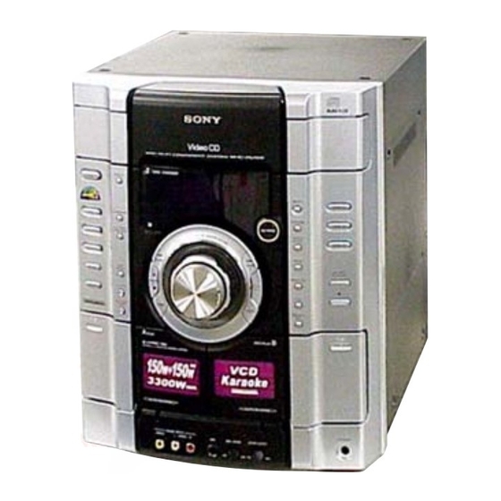
(Photo: HCD-RV55)
Model Name Using Similar Mechanism
CD
CD Mechanism Type
Section
Base Unit Name
Optical Pick-up Name
Model Name Using Similar Machanism
Q Q
TAPE
3
6 7
1 3
1 5
Section
Tape Mechanism Type
SPECIFICATIONS
Inputs
VIDEO/SAT IN (phono jacks) (HCD-RV55 only):
GAME INPUT AUDIO L/R (phono jacks):
GAME INPUT VIDEO (phono jack):
MIC (phone jack):
Outputs
PHONES (stereo phone jack):
VIDEO/SAT OUT (phono jacks) (HCD-RV55 only):
MINI Hi-Fi COMPONENT SYSTEM
co
.
9 4
2 8
E Model
NEW
CDM74-K4BD49
BU-K4BD49
KSM-213DHAP
HCD-GN700
HCD-RG330
0 5
8
2 9
9 4
2 8
CWM43RR35
CWM43FF13
voltage 450/250 mV,
impedance 47 kilohms
voltage 250 mV,
impedance 47 kilohms
1 Vp-p, 75ohms
sensitivity 1 mV,
impedance 10 kilohms
accepts headphones of
8 ohms or more
impedance 1 kilohm
– Continued on next page –
m
9 9
9 9
1
Advertisement
Table of Contents

Related Manuals for Sony HCD-RV55


Summary of Contents for Sony HCD-RV55
- Page 1 CWM43RR35 Tape Mechanism Type CWM43FF13 SPECIFICATIONS Amplifier section Inputs VIDEO/SAT IN (phono jacks) (HCD-RV55 only): HCD-RV55 voltage 450/250 mV, Front speaker impedance 47 kilohms The following measured at AC 120, 127, 220, 240 V, 50/60 Hz GAME INPUT AUDIO L/R (phono jacks):...
- Page 2 WITH MARK 0 ON THE SCHEMATIC DIAGRAMS AND IN Design and specifications are subject to change without THE PARTS LIST ARE CRITICAL TO SAFE OPERATION. notice. REPLACE THESE COMPONENTS WITH SONY PARTS WHOSE PART NUMBERS APPEAR AS SHOWN IN THIS MANUAL OR IN SUPPLEMENTS PUBLISHED BY SONY. http://www.xiaoyu163.com...
- Page 3 http://www.xiaoyu163.com HCD-RV22/RV55 3 7 63 1515 0 Notes on Chip Component Replacement NOTES ON LASER DIODE EMISSION CHECK • Never reuse a disconnected chip component. The laser beam on this model is concentrated so as to be focused on • Notice that the minus side of a tantalum capacitor may be the disc reflective surface by the objective lens in the optical pick- damaged by heat.
- Page 4 http://www.xiaoyu163.com HCD-RV22/RV55 3 7 63 1515 0 MODEL IDENTIFICATION PLAYABLE DISC You can playback the following discs on this system. The other – BACK PANEL – discs cannot be played back. List of playable discs Format of discs Disc logo Part No.
-
Page 5: Table Of Contents
3-8. Trans Board ............... 13 6-21. Schematic Diagram –Power Section (HCD-RV22)– ..46 3-9. Main Board ............... 14 6-22. Schematic Diagram –Power Section (HCD-RV55)– ..47 3-10. Amp Board ................ 14 6-23. Printed Wiring Board 3-11. BD49 Board ..............15 –Power Section (1/2) (HCD-RV55)–... -
Page 6: Service Note
http://www.xiaoyu163.com HCD-RV22/RV55 SECTION 1 SERVICE NOTE 3 7 63 1515 0 1-1. SERVICE POSITION OF CD MECHANISM DECK Remove the CD mechanism deck and place it on top of the pedestal as shown. Inspect the BD49 board in this set up. BD49 board CD mechanism deck L 13942296513... -
Page 7: General
http://www.xiaoyu163.com HCD-RV22/RV55 SECTION 2 GENERAL 3 7 63 1515 0 This section is extracted from instruction manual. L 13942296513 u163 http://www.xiaoyu163.com... - Page 8 http://www.xiaoyu163.com HCD-RV22/RV55 3 7 63 1515 0 L 13942296513 u163 http://www.xiaoyu163.com...
-
Page 9: Disassembly
http://www.xiaoyu163.com HCD-RV22/RV55 SECTION 3 DISASSEMBLY 3 7 63 1515 0 Note : Disassemble the unit in the order as shown below. 3-1. CASE (TOP) (Page 10) 3-2. CD DOOR (Page 10) 3-3. FRONT PANEL SECTION (Page 11) 3-4. CD MECHANISM DECK 3-5. -
Page 10: Case (Top)
http://www.xiaoyu163.com HCD-RV22/RV55 3 7 63 1515 0 Note : Follow the disassembly procedure in the numerical order given. 3-1. CASE (TOP) qd two screws (+BVTP 3 × 10) qh case (top) 7 two screws (case 3 TP2) qs case (side-L) 9 screw (+BVTP 3 ×... -
Page 11: Front Panel Section
http://www.xiaoyu163.com HCD-RV22/RV55 3 7 63 1515 0 3-3. FRONT PANEL SECTION qf screw (+BV (3 − CR)) 4 screw (+BVTP 3 × 8) qa CN304 (8P) qg CN301 (3P) 1 CN805 (2P) 3 CN823 (11P) 8 screw (+BVTP 3 × 10) 5 screw (+BVTP 3 ×... -
Page 12: Tape Mechanism Deck, Mic Board
http://www.xiaoyu163.com HCD-RV22/RV55 3 7 63 1515 0 3-5. TAPE MECHANISM DECK, MIC BOARD 4 two MIC knobs 3 tape mechanism deck 2 six screws 1 connector (+BVTP 2.6 × 8) jack bracket 5 two screws 7 MIC board (+BVTP 2.6 × 8) 6 two screws (+BVTP 3 ×... -
Page 13: Back Panel Section, Sub Trans Board
http://www.xiaoyu163.com HCD-RV22/RV55 3 7 63 1515 0 3-7. BACK PANEL SECTION, SUB TRANS BOARD qs back panel section qa SUB TRANS board 3 CN901 (2P) 7 two screws 0 two screws (+BVTP 3 × 10) (+BVTP 3 × 10) 8 screw 2 CN906 (7P) (+BVTP 3 ×... -
Page 14: Main Board
http://www.xiaoyu163.com HCD-RV22/RV55 3 7 63 1515 0 3-9. MAIN BOARD 4 MAIN board 1 CN907 (10P) MAIN board 3 CN441 2 two screws (+BVTP 3 × 8) L 13942296513 3-10. AMP BOARD 2 two screws (+BVTT 4 × 8) 3 screw 4 screw (+BVTP 3 ×... -
Page 15: Bd49 Board
http://www.xiaoyu163.com HCD-RV22/RV55 3 7 63 1515 0 3-11. BD49 BOARD 3 screw 1 CN101 (29P) (+BVTP 2.6 × 8 ) 4 gap tube 6 BD49 board 2 CN102 (16P) Remove soldering from the four points. L 13942296513 3-12. VCD CONNECT BOARD, VMP43GY BOARD 4 CN101 (29P) 5 two screws (+BVTP 2.6 ×... -
Page 16: Driver Board, Sw Board
http://www.xiaoyu163.com HCD-RV22/RV55 3 7 63 1515 0 3-13. DRIVER BOARD, SW BOARD 1 two screws (+BTTP (M2.6)) 3 CN703 (4P) 4 DRIVER board 5 screw (+BTTP (M2.6)) 6 SW board 2 CN702 (5P) L 13942296513 3-14. OPTICAL PICK-UP 3 insulator 8 optical pick-up 2 coil spring (BU-K4BD49) -
Page 17: Sensor Board
http://www.xiaoyu163.com HCD-RV22/RV55 3 7 63 1515 0 3-15. SENSOR BOARD 1 floating screw (+PTPWH M2.6) 2 t ray 8 s crew (+BTTP (M2.6)) 3 b elt (table) 0 SENSOR board 4 floating screw (+PTPWH M2.6) 5 p ulley (table) 6 floating screw 9 CN731 (3P) (+PTPWH M2.6) 7 g ear (geneva) -
Page 18: Motor (Ld) Board
http://www.xiaoyu163.com HCD-RV22/RV55 3 7 63 1515 0 3-17. MOTOR (LD) BOARD 2 two screws (+BTTP (M2.6)) 4 Remove the two solderings of motor. 3 MOTOR (LD) board 5 l oading motor assy (M751) 1 b elt (loading) L 13942296513 u163 http://www.xiaoyu163.com... -
Page 19: Test Mode
http://www.xiaoyu163.com HCD-RV22/RV55 SECTION 4 TEST MODE 3 7 63 1515 0 MC COLD RESET CD TRAY LOCK MODE The cold reset clears all data including preset data stored in the This mode is used to unable to take sample disc out of tray in the RAM to initial conditions. - Page 20 http://www.xiaoyu163.com HCD-RV22/RV55 3 7 63 1515 0 AGING MODE 3. Tape Deck Section The sequence during the aging mode is following as below. This mode can be used for operation check of CD section and tape If an error occurred, stop display that step. deck section.
- Page 21 http://www.xiaoyu163.com HCD-RV22/RV55 3 7 63 1515 0 MC TEST MODE 1. Mechanism Deck Error Code Mode When this mode is entered, mechanism deck error code is displayed This mode is used to check operations of microprocessor. with the 10-character format on the fluorescent indicator tube. Procedure: 1.
- Page 22 http://www.xiaoyu163.com HCD-RV22/RV55 3 7 63 1515 0 The 7th and 8th digit from the left indicates: The 5th and 6th digit from the left indicates: (Motor status display) (Error step display) The 7th and 8th digit from the left indicates which motor output The 5th and 6th digit from the left indicates which processing when status when an error occurred is indicated.
-
Page 23: Electrical Adjustments
http://www.xiaoyu163.com HCD-RV22/RV55 SECTION 5 ELECTRICAL ADJUSTMENTS 3 7 63 1515 0 Note: Clear RF signal waveform means that the shape “ ◊ ” can be clearly CD SECTION distinguished at the center of the waveform. Note: RF signal waveform 1. CD Block is basically designed to operate without adjustment. VOLT/DIV : 200mV Therefore, check each item in order given. - Page 24 http://www.xiaoyu163.com HCD-RV22/RV55 3 7 63 1515 0 VIDEO SECTION AUDIO LEVEL, VIDEO CLOCK, AUDIO SERVO – VMP43GY BOARD (Component Side) – CLOCK CHECK level meter VMP43GY board TP415 (L-OUT) TP413 (R-OUT) – TP70 frequency counter VMP43GY board (54 MHz) TP70 (54 MHz) TP182 (4.2336 MHz) –...
-
Page 25: Diagrams
http://www.xiaoyu163.com HCD-RV22/RV55 SECTION 6 DIAGRAMS 3 7 63 1515 0 6-1. CIRCUIT BOARDS LOCATION VMP43GY board SENSOR board BD49 board SW board MOTOR (TB) board MOTOR (LD) board DRIVER board VCD CONNECT board TRANS board AMP board L 13942296513 VIDEO OUT board SUB TRANS board REM board PANEL board... - Page 26 http://www.xiaoyu163.com HCD-RV22/RV55 3 7 63 1515 0 • NOTE FOR PRINTED WIRING BOARDS AND SCHEMATIC DIAGRAMS Note on Printed Wiring Board: Note on Schematic Diagram: • X : parts extracted from the component side. • All capacitors are in µF unless otherwise noted. (p: pF) •...
- Page 27 http://www.xiaoyu163.com HCD-RV22/RV55 3 7 6 3 1 5 1 5 0 • Waveforms – BD49 Board – – VMP43GY Board – – PANEL Board – IC103 qg (RFAC) IC504 1 (BCK), IC505 os (L CDBCK), IC505 <zmc (RFAC) IC601 qd (I-XT2) (CD Play Mode) IC505 <x/c (AUDBCK) od (BCK)
-
Page 28: Printed Wiring Board -Cd Mechanism Section (1/2)
http://www.xiaoyu163.com HCD-RV22/RV55 3 7 6 3 1 5 1 5 0 6-2. PRINTED WIRING BOARD — CD MECHANISM SECTION (1/2) — • Refer to page 25 for Circuit Boards Location. : Uses unleaded solder. 1 3 9 4 2 2 9 6 5 1 3 (Page 33) •... -
Page 29: Schematic Diagram -Cd Mechanism Section (1/2)
http://www.xiaoyu163.com HCD-RV22/RV55 3 7 6 3 1 5 1 5 0 • Refer to page 27 for Waveforms. 6-3. SCHEMATIC DIAGRAM — CD MECHANISM SECTION (1/2) — • Refer to page 50 for IC Block Diagram. TP11 C121 TP18 FB111 C119 C118 CN102... -
Page 30: Printed Wiring Boards -Cd Mechanism Section (2/2)
http://www.xiaoyu163.com HCD-RV22/RV55 3 7 6 3 1 5 1 5 0 6-4. PRINTED WIRING BOARDS — CD MECHANISM SECTION (2/2) — • Refer to page 25 for Circuit Boards Location. : Uses unleaded solder. 1 3 9 4 2 2 9 6 5 1 3 MAIN BOARD CN301... -
Page 31: Schematic Diagram -Cd Mechanism Section (2/2)
http://www.xiaoyu163.com HCD-RV22/RV55 3 7 6 3 1 5 1 5 0 6-5. SCHEMATIC DIAGRAM — CD MECHANISM SECTION (2/2) — • Refer to page 50 for IC Block Diagrams. IC B/D IC701 R702 R701 D701 C715 CN704 C751 CN721 M751 IC B/D IC712 R712... -
Page 32: Printed Wiring Board -Vcd Connect Section
http://www.xiaoyu163.com HCD-RV22/RV55 3 7 6 3 1 5 1 5 0 6-6. PRINTED WIRING BOARD — VCD CONNECT SECTION — 6-7. SCHEMATIC DIAGRAM — VCD CONNECT SECTION — • Refer to page 25 for Circuit Boards Location. • : Uses unleaded solder. (Page 39) CN883 JW882... -
Page 33: Printed Wiring Board -Vmp Section
http://www.xiaoyu163.com HCD-RV22/RV55 3 7 6 3 1 5 1 5 0 6-8. PRINTED WIRING BOARD — VMP SECTION — • Refer to page 25 for Circuit Boards Location. : Uses unleaded solder. (Page 32) • Semiconductor Location Ref. No. Location IC102 IC201 IC202... -
Page 34: Schematic Diagram -Vmp Section (1/2)
http://www.xiaoyu163.com HCD-RV22/RV55 3 7 6 3 1 5 1 5 0 • Refer to page 27 for Waveforms. 6-9. SCHEMATIC DIAGRAM — VMP SECTION (1/2) — • Refer to page 50 for IC Block Diagrams. R152 C155 R158 C154 TP419 TP418 TP417 C258... -
Page 35: Schematic Diagram -Vmp Section (2/2)
http://www.xiaoyu163.com HCD-RV22/RV55 3 7 6 3 1 5 1 5 0 • Refer to page 27 for Waveforms. 6-10. SCHEMATIC DIAGRAM — VMP SECTION (2/2) — • Refer to page 52 for IC Pin Description of IC505. FL503 FL504 FB501 FB504 FB503 TP197 TP177... -
Page 36: Schematic Diagram -Main Section (1/2)
http://www.xiaoyu163.com HCD-RV22/RV55 3 7 6 3 1 5 1 5 0 6-11. SCHEMATIC DIAGRAM — MAIN SECTION (1/2) — • Refer to page 51 for IC Block Diagram. C167 C172 C171 R145 R143 CN309 Q372 R144 C169 R146 R391 R386 C173 R149 C156... -
Page 37: Schematic Diagram -Main Section (2/2)
http://www.xiaoyu163.com HCD-RV22/RV55 3 7 6 3 1 5 1 5 0 • Refer to page 51 for IC Block Diagrams. 6-12. SCHEMATIC DIAGRAM — MAIN SECTION (2/2) — • Refer to page 57 for IC Pin Description of IC371. (Page 36) Q362 C270 R361... -
Page 38: Printed Wiring Board -Main Section
http://www.xiaoyu163.com HCD-RV22/RV55 3 7 6 3 1 5 1 5 0 6-13. PRINTED WIRING BOARD — MAIN SECTION — • Refer to page 25 for Circuit Boards Location. : Uses unleaded solder. (Page 30) (Page 32) (Page 42) • Semiconductor Location Ref. -
Page 39: Printed Wiring Boards -Panel Section
http://www.xiaoyu163.com HCD-RV22/RV55 3 7 6 3 1 5 1 5 0 6-14. PRINTED WIRING BOARDS — PANEL SECTION — • Refer to page 25 for Circuit Boards Location. : Uses unleaded solder. IC610 (Page 32) 1 3 9 4 2 2 9 6 5 1 3 (Page 38) (Page 42) (Page 42) -
Page 40: Schematic Diagram -Panel Section (1/2)
http://www.xiaoyu163.com HCD-RV22/RV55 3 7 6 3 1 5 1 5 0 6-15. SCHEMATIC DIAGRAM — PANEL SECTION (1/2) — CN605 R704 R706 R708 R700 JW660 R702 JW659 (Page 43) Q610 Q612 Q611 Q614 Q615 Q613 R698 CN604 JW674 JW718 (Page 43) JW705 JW655 JW656... -
Page 41: Schematic Diagram -Panel Section (2/2)
http://www.xiaoyu163.com HCD-RV22/RV55 3 7 6 3 1 5 1 5 0 • Refer to page 27 for Waveforms. 6-16. SCHEMATIC DIAGRAM — PANEL SECTION (2/2) — • Refer to page 58 for IC Pin Description of IC601. FL601 CN603 C623 C622 R780 R779... -
Page 42: Printed Wiring Boards -Jack Section
http://www.xiaoyu163.com HCD-RV22/RV55 3 7 6 3 1 5 1 5 0 6-17. PRINTED WIRING BOARDS — JACK SECTION — • Refer to page 25 for Circuit Boards Location. : Uses unleaded solder. (Page 38) (Page 39) (Page 38) (Page 39) 1 3 9 4 2 2 9 6 5 1 3 J803 C840... -
Page 43: Schematic Diagram -Jack Section
http://www.xiaoyu163.com HCD-RV22/RV55 3 7 6 3 1 5 1 5 0 6-18. SCHEMATIC DIAGRAM — JACK SECTION — S660 C830 C831 SW601 CN804 J801 R673 (Page 36) C832 W803 CN606 CN607 (Page 40) (Page 40) C833 IC803 CN808 JK802 C859 IC801(1/2) R832 C811... -
Page 44: Printed Wiring Board -Power Section (1/2) (Hcd-Rv22)
http://www.xiaoyu163.com HCD-RV22/RV55 3 7 6 3 1 5 1 5 0 6-19. PRINTED WIRING BOARD — POWER SECTION (1/2) (HCD-RV22) — • Refer to page 25 for Circuit Boards Location. : Uses unleaded solder. 1 3 9 4 2 2 9 6 5 1 3 •... -
Page 45: Printed Wiring Boards -Power Section (2/2) (Hcd-Rv22)
http://www.xiaoyu163.com HCD-RV22/RV55 3 7 6 3 1 5 1 5 0 6-20. PRINTED WIRING BOARDS — POWER SECTION (2/2) (HCD-RV22) — • Refer to page 25 for Circuit Boards Location. : Uses unleaded solder. (Page 44) 1 3 9 4 2 2 9 6 5 1 3 (Page 38) •... -
Page 46: Schematic Diagram -Power Section (Hcd-Rv22)
http://www.xiaoyu163.com HCD-RV22/RV55 3 7 6 3 1 5 1 5 0 6-21. SCHEMATIC DIAGRAM — POWER SECTION (HCD-RV22) — JW403 L441 R451 RY441 C441 R441 R461 JW441 IC441(1/2) C445 R413 R462 R466 R465 R411 TH441 L442 R447 D443 EP491 Q483 JK441 R485 R483... -
Page 47: Schematic Diagram -Power Section (Hcd-Rv55)
HCD-RV22/RV55 3 7 6 3 1 5 1 5 0 6-22. SCHEMATIC DIAGRAM — POWER SECTION (HCD-RV55) — C461 R467 D445 R496 L441 R449 RY441 C441 R474 R411 R441 R461 Q491 JW441 R462 IC441(1/2) R466 R465 C445 JW403 L442... -
Page 48: Printed Wiring Board -Power Section (1/2) (Hcd-Rv55)
HCD-RV22/RV55 3 7 6 3 1 5 1 5 0 6-23. PRINTED WIRING BOARD — POWER SECTION (1/2) (HCD-RV55) — • Refer to page 25 for Circuit Boards Location. : Uses unleaded solder. 1 3 9 4 2 2 9 6 5 1 3 •... -
Page 49: Printed Wiring Boards -Power Section (2/2) (Hcd-Rv55)
HCD-RV22/RV55 6-24. PRINTED WIRING BOARDS — POWER SECTION (2/2) (HCD-RV55) — • Refer to page 25 for Circuit Boards Location. : Uses unleaded solder. 3 7 6 3 1 5 1 5 0 LP903 D904 D905 JW911 CN906 CN904... -
Page 50: Ic Block Diagrams
http://www.xiaoyu163.com HCD-RV22/RV55 3 7 6 3 1 5 1 5 0 6-25. IC BLOCK DIAGRAMS IC504 PCM1748E/2K (VMP43GY BOARD) IC103 CXA2581N-T4 (BD49 BOARD) 15 14 RW/ROM ZERO DETECT DC OFST RFDCI – SYSTEM – FUNCTION CLOCK OUTPUT AMP AND RFDCO CONTROL MANAGER CONVERTER... - Page 51 http://www.xiaoyu163.com HCD-RV22/RV55 3 7 63 1515 0 IC101 BD3401KS2 (MAIN BOARD) VOLOUT2 TNF2 BASS MIDDLE TREBLE TNF1 BBNF2 SUR1 BBIN2 BASS MIDDLE TREBLE SURROUND SUR2 fc=100HZ LINEOUT2 LINEOUT1 BUFFER MIC MIX SAOUT2 VOCAL FADER SWOUT SAOUT1 FILTER 1/2 Vcc GAME L L 13942296513 GAME R TUNER L...
- Page 52 http://www.xiaoyu163.com HCD-RV22/RV55 3 7 63 1515 0 • IC Pin Function Description • IC505 CXD1887R (DIGITAL SIGNAL PROCESSOR, DIGITAL SERVO PROCESSOR, MPEG VIDEO/AUDIO DECODER, VIDEO SIGNAL ENCODER) (VMP43GY BOARD (2/2)) Pin No. Pin Name Pin Description Connected to ground via a capacitor. IREF D/A converter reference current output D/A converter reference voltage input...
- Page 53 http://www.xiaoyu163.com HCD-RV22/RV55 3 7 63 1515 0 Pin No. Pin Name Pin Description IVS4 — Ground pin (for I/O) DRCAS Column address strobe signal output to the D-RAM LVD4 — Digital power supply pin (+2.5 V) (for AV decoder block) DRCK Clock signal output to the D-RAM IVD5...
- Page 54 http://www.xiaoyu163.com HCD-RV22/RV55 3 7 63 1515 0 Pin No. Pin Name Pin Description L SENS SENS signal input SENS SENS signal output L SLCK SENS serial data readout clock signal output SCLK SENS serial data readout clock signal input VDD3 —...
- Page 55 http://www.xiaoyu163.com HCD-RV22/RV55 3 7 63 1515 0 Pin No. Pin Name Pin Description AVS0 — Analog ground pin ADIO Output for the test Not used. RFDC RF signal input from the RF amplifier Center servo analog signal input Tracking error signal input from the RF amplifier Sled error signal input from the RF amplifier Focus error signal input from the RF amplifier Center voltage (+1.65 V) input...
- Page 56 http://www.xiaoyu163.com HCD-RV22/RV55 3 7 63 1515 0 Pin No. Pin Name Pin Description AUDDTO1 Serial audio data output Not used. (Open) AUDBCK Serial audio bit clock signal (2.8224 MHz) output to the digital filter AUDLRCK Serial audio L/R sampling clock signal (44.1 kHz) output to the digital filter AUDXCLKO Serial audio clock signal output to the digital filter CLKA...
- Page 57 http://www.xiaoyu163.com HCD-RV22/RV55 3 7 63 1515 0 • IC371 BU2099FV (SP DRIVER) (MAIN BOARD (2/2)) Pin No. Pin Name Pin Description — Ground pin N.C. — Not used. (Open) DATA Serial data input from the motor/plunger driver CLOCK Serial data transfer clock signal input from the system controller Latch pulse signal input from the system controller Recording/playback selection signal output Recording bias control signal output...
- Page 58 http://www.xiaoyu163.com HCD-RV22/RV55 3 7 63 1515 0 • IC601 LC876964C-52S6-E (SYSTEM CONTROLLER) (PANEL BOARD (2/2)) Pin No. Pin Name Pin Description O-MP3 CS CS signal output to CD digital processor O-MP3 LP LP signal output to CD digital processor and motor signal output I-MP3 ACK ACK signal input from CD digital processsor and motor signal input O-MP3 REQ...
- Page 59 http://www.xiaoyu163.com HCD-RV22/RV55 3 7 63 1515 0 Pin No. Pin Name Pin Description STREAM-LED4 Illumination LED control signal output STREAM-LED3 Illumination LED control signal output STREAM-LED2 Illumination LED control signal output STREAM-LED1 Illumination LED control signal output I-LC72121 DI Data signal input from tuner O-LC72121 CE Chip select signal output to tuner O-LC72121/BU2099FV DO...
-
Page 60: Exploded Views
http://www.xiaoyu163.com HCD-RV22/RV55 SECTION 7 EXPLODED VIEWS 3 7 63 1515 0 NOTE: • The mechanical parts with no reference • Accessories are given in the last of this The components identified by mark 0 or dotted line with mark number in the exploded views are not supplied. parts list. -
Page 61: Front Panel Section (1)
http://www.xiaoyu163.com HCD-RV22/RV55 3 7 63 1515 0 7-2. FRONT PANEL SECTION (1) not supplied (REM board) FL601 not supplied L 13942296513 not supplied not supplied not supplied (H/P JACK board) Ref. No. Part No. Description Remark Ref. No. Part No. Description Remark 4-951-620-01 SCREW (2.6X8), +BVTP... -
Page 62: Front Panel Section (2)
http://www.xiaoyu163.com HCD-RV22/RV55 3 7 63 1515 0 7-3. FRONT PANEL SECTION (2) not supplied not supplied L 13942296513 Ref. No. Part No. Description Remark Ref. No. Part No. Description Remark 4-231-841-01 SPRING (HEART CAM-B) 4-231-824-01 CAM (A), HEART 4-231-825-01 CAM (B), HEART 4-231-836-01 SPRING (HEART CAM-A) 4-224-104-11 DAMPER 4-252-218-11 BUTTON, VIDEO/SAT... -
Page 63: Q Q
http://www.xiaoyu163.com HCD-RV22/RV55 3 7 63 1515 0 7-4. FRONT PANEL SECTION (3) not supplied not supplied not supplied supplied not supplied (6 STREAM LED board) not supplied L 13942296513 not supplied not supplied Ref. No. Part No. Description Remark Ref. No. Part No. -
Page 64: Main Board Section
http://www.xiaoyu163.com HCD-RV22/RV55 3 7 63 1515 0 7-5. MAIN BOARD SECTION not supplied not supplied PT901 not supplied (TRANS board) not supplied FC901 F905 F906 F908 F909 F907 F904 L 13942296513 not supplied The components identified by mark 0 or dotted line with mark 0 are critical for safety. -
Page 65: Cd Mechanism Deck Section (1)
http://www.xiaoyu163.com HCD-RV22/RV55 3 7 63 1515 0 7-6. CD MECHANISM DECK SECTION (1) (CDM74-K4BD49) M741 L 13942296513 CD mechanism deck section -2 Ref. No. Part No. Description Remark Ref. No. Part No. Description Remark 4-243-816-01 TRAY 1-776-182-11 WIRE (FLAT TYPE) (5 CORE) 4-218-252-61 SCREW (+PTPWH M2.6), FLOATING 1-687-134-12 MOTOR (TB) BOARD 4-218-253-22 SCREW (M2.6), +BTTP... -
Page 66: Cd Mechanism Deck Section (2)
http://www.xiaoyu163.com HCD-RV22/RV55 3 7 63 1515 0 7-7. CD MECHANISM DECK SECTION (2) (CDM74-K4BD49) RE701 M751 CD mechanism deck section -3 L 13942296513 not supplied (VCD CONNECT board) Ref. No. Part No. Description Remark Ref. No. Part No. Description Remark 4-218-252-61 SCREW (+PTPWH M2.6), FLOATING 4-244-108-01 GEAR, SWING 4-244-034-01 BELT (LOADING) -
Page 67: Cd Mechanism Deck Section (3)
http://www.xiaoyu163.com HCD-RV22/RV55 3 7 63 1515 0 7-8. CD MECHANISM DECK SECTION (3) (CDM74-K4BD49) L 13942296513 BU-K4BD49 Ref. No. Part No. Description Remark Ref. No. Part No. Description Remark X-4955-774-2 PULLEY (SM) ASSY, CHUCKING 4-231-151-01 STOPPER (BU) 1-471-035-11 MAGNET ASSY 4-218-253-32 SCREW (M2.6), +BTTP 4-221-688-01 PULLEY (B), CHUCKING 4-985-672-01 SCREW (+PTPWH M2.6), FLOATING... -
Page 68: Base Unit Section
http://www.xiaoyu163.com HCD-RV22/RV55 3 7 63 1515 0 7-9. BASE UNIT SECTION (BU-K4BD49) not supplied L 13942296513 The components identified by mark 0 or dotted line with mark 0 are critical for safety. Replace only with part number specified. Ref. No. Part No. -
Page 69: Electrical Parts List
http://www.xiaoyu163.com HCD-RV22/RV55 SECTION 8 ELECTRICAL PARTS LIST 3 7 63 1515 0 NOTE: • Due to standardization, replacements in • Items marked “*” are not stocked since The components identified by mark 0 or dotted line with mark the parts list may be different from the they are seldom required for routine service. - Page 70 http://www.xiaoyu163.com HCD-RV22/RV55 3 7 63 1515 0 Ref. No. Part No. Description Remark Ref. No. Part No. Description Remark < TERMINAL BOARD > R447 1-249-437-11 CARBON 1/4W (RV22) JK441 1-694-877-21 TERMINAL BOARD (8P) (FRONT SPEAKER, R447 1-249-438-11 CARBON 1/4W SURROUND SPEAKER) (RV55) (RV55) JK441 1-694-884-11 TERMINAL BOARD (4P) (SPEAKER) (RV22)
- Page 71 http://www.xiaoyu163.com HCD-RV22/RV55 BD49 3 7 63 1515 0 Ref. No. Part No. Description Remark Ref. No. Part No. Description Remark 0 R477 1-212-881-11 FUSIBLE 1/4W F < JUPER RESISTOR > (RV55) R478 1-249-429-11 CARBON 1/4W C213 1-216-864-11 SHORT CHIP (RV55) R481 1-247-847-91 CARBON 4.7K...
- Page 72 http://www.xiaoyu163.com HCD-RV22/RV55 BD49 DRIVER H/P JACK MAIN 3 7 63 1515 0 Ref. No. Part No. Description Remark Ref. No. Part No. Description Remark < SWITCH > H/P JACK BOARD ************** S101 1-771-853-11 SWITCH, DETECTION (LIMIT) < CAPACITOR > ************************************************************* 1-687-135-12 DRIVER BOARD C830 1-162-964-11 CERAMIC CHIP...
- Page 73 http://www.xiaoyu163.com HCD-RV22/RV55 MAIN 3 7 63 1515 0 Ref. No. Part No. Description Remark Ref. No. Part No. Description Remark C139 1-131-690-31 FILM 0.068uF C213 1-126-964-11 ELECT 10uF C140 1-131-690-31 FILM 0.068uF C214 1-126-926-11 ELECT 1000uF C141 1-126-964-11 ELECT 10uF C216 1-164-156-11 CERAMIC CHIP 0.1uF...
- Page 74 http://www.xiaoyu163.com HCD-RV22/RV55 MAIN 3 7 63 1515 0 Ref. No. Part No. Description Remark Ref. No. Part No. Description Remark C374 1-126-947-11 ELECT 47uF IC301 6-702-771-01 IC TA78033LS C375 1-164-156-11 CERAMIC CHIP 0.1uF IC302 8-759-231-53 IC TA7805S C376 1-126-961-11 ELECT 2.2uF IC303 8-759-701-59 IC NJM78M09FA...
- Page 75 http://www.xiaoyu163.com HCD-RV22/RV55 MAIN 3 7 63 1515 0 Ref. No. Part No. Description Remark Ref. No. Part No. Description Remark R111 1-216-843-11 METAL CHIP 1/10W R165 1-216-833-11 METAL CHIP 1/10W (RV55) R166 1-216-833-11 METAL CHIP 1/10W R111 1-216-846-11 METAL CHIP 120K 1/10W R167...
- Page 76 http://www.xiaoyu163.com HCD-RV22/RV55 MAIN 3 7 63 1515 0 Ref. No. Part No. Description Remark Ref. No. Part No. Description Remark R235 1-216-793-11 METAL CHIP 1/10W R343 1-216-837-11 METAL CHIP 1/10W R241 1-216-797-11 METAL CHIP 1/10W R344 1-216-837-11 METAL CHIP 1/10W (RV22) R345 1-216-833-11 METAL CHIP...
- Page 77 http://www.xiaoyu163.com HCD-RV22/RV55 MOTOR (LD) 3 7 63 1515 0 Ref. No. Part No. Description Remark Ref. No. Part No. Description Remark C820 1-162-923-11 CERAMIC CHIP 47PF < TRANSISTOR > C821 1-164-156-11 CERAMIC CHIP 0.1uF C822 1-164-315-11 CERAMIC CHIP 470PF Q801 8-729-120-28 TRANSISTOR 2SC1623-L5L6 C823 1-115-416-11 CERAMIC CHIP...
- Page 78 http://www.xiaoyu163.com HCD-RV22/RV55 MOTOR (TB) PANEL 3 7 63 1515 0 Ref. No. Part No. Description Remark Ref. No. Part No. Description Remark 1-687-134-12 MOTOR (TB) BOARD < CONNECTOR > ***************** CN601 1-784-751-11 CONNECTOR, FFC 29P < CONNECTOR > CN602 1-784-774-11 CONNECTOR, FFC 13P CN603 1-568-830-11 CONNECTOR, FFC 11P CN742...
- Page 79 http://www.xiaoyu163.com HCD-RV22/RV55 PANEL 3 7 63 1515 0 Ref. No. Part No. Description Remark Ref. No. Part No. Description Remark Q604 8-729-119-76 TRANSISTOR 2SA1175-HFE R651 1-216-833-11 METAL CHIP 1/10W Q605 8-729-120-28 TRANSISTOR 2SC1623-L5L6 R652 1-216-835-11 METAL CHIP 1/10W Q606 8-729-027-55 TRANSISTOR DTC143EKA-T146 R653 1-216-817-11 METAL CHIP 1/10W...
- Page 80 http://www.xiaoyu163.com HCD-RV22/RV55 PANEL 3 7 63 1515 0 Ref. No. Part No. Description Remark Ref. No. Part No. Description Remark R717 1-216-827-11 METAL CHIP 3.3K 1/10W R784 1-216-809-11 METAL CHIP 1/10W R718 1-216-837-11 METAL CHIP 1/10W R786 1-216-833-11 METAL CHIP 1/10W R719 1-216-827-11 METAL CHIP...
- Page 81 http://www.xiaoyu163.com HCD-RV22/RV55 SENSOR SUB TRANS TRANS VCD CONNECT 3 7 63 1515 0 Ref. No. Part No. Description Remark Ref. No. Part No. Description Remark REM BOARD TRANS BOARD *********** ************ < CONNECTOR > 1-533-217-41 HOLDER, FUSE CN610 1-816-423-11 SOCKET, CONNECTOR 3P <...
- Page 82 http://www.xiaoyu163.com HCD-RV22/RV55 VIDEO OUT VMP43GY 3 7 63 1515 0 Ref. No. Part No. Description Remark Ref. No. Part No. Description Remark VIDEO OUT BOARD C361 1-162-964-11 CERAMIC CHIP 0.001uF (RV22:EA) **************** C361 1-164-156-11 CERAMIC CHIP 0.1uF < CAPACITOR > (EXCEPT RV22:EA) C362 1-162-927-11 CERAMIC CHIP...
- Page 83 http://www.xiaoyu163.com HCD-RV22/RV55 VMP43GY 3 7 63 1515 0 Ref. No. Part No. Description Remark Ref. No. Part No. Description Remark C574 1-164-156-11 CERAMIC CHIP 0.1uF < RESISTOR > C575 1-126-206-11 ELECT CHIP 100uF 6.3V C576 1-126-206-11 ELECT CHIP 100uF 6.3V R102 1-216-809-11 METAL CHIP 1/10W...
- Page 84 http://www.xiaoyu163.com HCD-RV22/RV55 VMP43GY 6 STREAM 3 7 63 1515 0 Ref. No. Part No. Description Remark Ref. No. Part No. Description Remark R561 1-216-821-11 METAL CHIP 1/10W MISCELLANEOUS R581 1-216-809-11 METAL CHIP 1/10W *************** R582 1-216-817-11 METAL CHIP 1/10W 1-769-940-11 WIRE (FLAT TYPE) (11 CORE) <...
- Page 85 http://www.xiaoyu163.com HCD-RV22/RV55 3 7 63 1515 0 MEMO L 13942296513 u163 http://www.xiaoyu163.com...
- Page 86 http://www.xiaoyu163.com HCD-RV22/RV55 3 7 63 1515 0 REVISION HISTORY Clicking the version allows you to jump to the revised page. Also, clicking the version at the upper on the revised page allows you to jump to the next revised page. Ver.
Need help?
Do you have a question about the HCD-RV55 and is the answer not in the manual?
Questions and answers