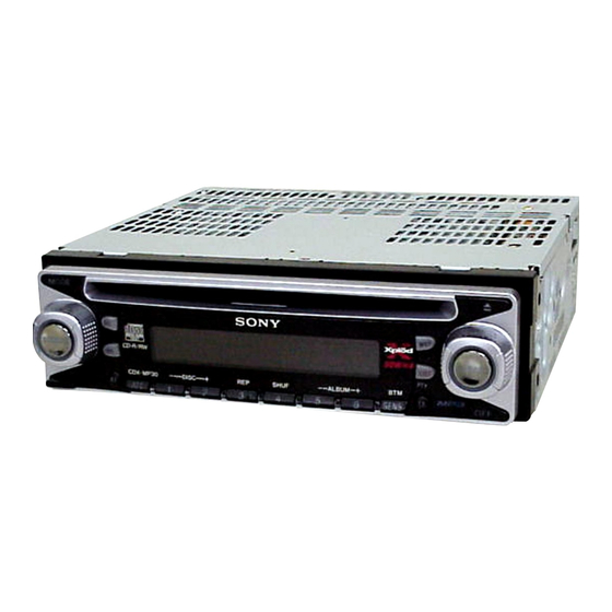
Sony CDX-MP30 Service Manual
Fm/am (mw/lw) compact disc player
Hide thumbs
Also See for CDX-MP30:
- Operating instruction (152 pages) ,
- Operating instructions manual (81 pages) ,
- Installation/connections (5 pages)
Table of Contents
Advertisement
Quick Links
SERVICE MANUAL
Ver 1.0 2002. 03
• The tuner and CD sections have no adjustments.
AUDIO POWER SPECIFICATIONS (US model)
POWER OUTPUT AND TOTAL HARMONIC DISTORTION 23 watts per channel minimum continuous average power into 4 ohms, 4 channels
driven from 20 Hz to 20 kHz with no more than 5% total harmonic distortion.
CD player section
Signal-to-noise ratio
90 dB
Frequency response
10 – 20,000 Hz
Wow and flutter
Below measurable limit
Tuner section
FM
Tuning range
US model
87.5 – 107.9 MHz
AEP and E models
87.5 – 108.0 MHz
Antenna terminal
US model
External antenna connector
AEP and E models
External aerial connector
Intermediate frequency
US model
10.7 MHz
AEP and E models
10.7 MHz/450 kHz
Usable sensitivity
US model
11 dBf
AEP and E models
8 dBf
Selectivity
75 dB at 400 kHz
Signal-to-noise ratio
US model
65 dB (stereo),
68 dB (mono)
AEP and E models
66 dB (stereo),
72 dB (mono)
Harmonic distortion at 1 kHz
US model
0.7% (stereo),
0.5% (mono)
AEP and E models
0.6% (stereo),
0.3% (mono)
Sony Corporation
9-873-924-01
2002C1600-1
e Vehicle Company
© 2002.03
Published by Sony Engineering Corporation
CDX-MP30
Photo: AEP model
Model Name Using Similar Mechanism
CD Drive Mechanism Type
Optical Pick-up Name
SPECIFICATIONS
Separation
US model
33 dB at 1 kHz
AEP and E models
35 dB at 1 kHz
Frequency response
30 – 15,000 Hz
AM (US model)
Tuning range
530 – 1,710 kHz
Antenna terminal
External antenna connector
Intermediate frequency 10.7 MHz/450 kHz
30 µV
Sensitivity
MW/LW (AEP and E models)
Tuning range
MW : 531 – 1,602 kHz
LW : 153 – 279 kHz
Aerial terminal
External aerial connector
Intermediate frequency 10.7 MHz/450 kHz
MW : 30 µV
Sensitivity
LW : 40 µV
Power amplifier section
Outputs
Speaker outputs
(sure seal connectors)
Speaker impedance
4 – 8 ohms
Maximum power output
52 W × 4 (at 4 ohms)
US model
50 W × 4 (at 4 ohms)
AEP and E models
FM/AM (MW/LW) COMPACT DISC PLAYER
US Model
AEP Model
E Model
New
MG-393M-121
KSS-720A
General
Outputs
US model
Power antenna relay control lead
AEP and E models
Power aerial relay control lead
Input
Telephone ATT control lead
Tone controls
Bass ±10 dB at 20 Hz
US model
Treble ±10 dB at 20 kHz
Bass ±9 dB at 100 Hz
AEP and E models
Treble ±9 dB at 10 kHz
Power requirements
12 V DC car battery
(negative earth)
Approx. 178 × 50 × 177 mm
Dimensions
× 2
× 7 in.)
1
1
(7
/
/
8
8
(w/h/d)
Approx. 182 × 53 × 161 mm
Mounting dimensions
× 2 × 6
1
3
(7
/
/
in.)
4
8
(w/h/d)
Mass
Approx. 1.2 kg
Supplied accessories
Parts for installation and
connections (1 set)
Front panel case (1)
Note
This unit cannot be connected to a digital preamplifier
or an equalizer.
Design and specifications are subject to change without
notice.
Advertisement
Table of Contents

Related Manuals for Sony CDX-MP30


Summary of Contents for Sony CDX-MP30
-
Page 1: Specifications
0.7% (stereo), Design and specifications are subject to change without 0.5% (mono) notice. AEP and E models 0.6% (stereo), 0.3% (mono) FM/AM (MW/LW) COMPACT DISC PLAYER Sony Corporation 9-873-924-01 2002C1600-1 e Vehicle Company © 2002.03 Published by Sony Engineering Corporation... - Page 2 COMPONENTS IDENTIFIED BY MARK 0 OR DOTTED LINE WITH MARK 0 ON THE SCHEMATIC DIAGRAMS AND IN THE PARTS LIST ARE CRITICAL TO SAFE OPERATION. REPLACE THESE COMPONENTS WITH SONY PARTS WHOSE PART NUMBERS APPEAR AS SHOWN IN THIS MANUAL OR IN SUPPLEMENTS PUBLISHED BY...
-
Page 3: Table Of Contents
CDX-MP30 TABLE OF CONTENTS 1. GENERAL 3. DIAGRAMS Location of controls (US model) ..........4 3-1. Block Diagram –CD Section– ........13 Location of controls (AEP and E model) ....... 4 3-2. Block Diagram –MAIN Section– ......14 Connections (US and E model) ..........5 3-3. -
Page 4: General
CDX-MP30 SECTION 1 GENERAL This section is extracted from instruction manual. (US model) (AEP and E model) -
Page 5: Connections (Us And E Model)
CDX-MP30 Connection (US and E model) Source selector (not supplied) Sélecteur de source Supplied with the CD/MD changer (non fourni) Fourni avec le changeur de CD/MD Selector de fuente Suministrado con el cambiador de CD/MD (no suministrado) Supplied with XA-C30... -
Page 6: Connections (Aep Model)
CDX-MP30 Connection (AEP model) Note for the aerial connecting Nota per il collegamento dell’antenna If your car aerial is an ISO (International Se l’antenna dell’auto è di tipo ISO Organisation for Standardisation) type, (International Organization use the supplied adaptor 6 to connect it. -
Page 7: Disassembly
CDX-MP30 SECTION 2 DISASSEMBLY Note : This set can be disassemble according to the following sequence. 2-6. CHASSIS (T) SUB ASSY 2-1. COVER (Page 10) (Page 7) 2-7. LEVER SECTION 2-8. SERVO BOARD 2-2. PANEL (1) ASSY, SUB (Page 10) -
Page 8: Panel (1) Assy, Sub
CDX-MP30 2-2. Panel (1) Assy, Sub 5 three claws 3 claw 1 screw ( PTT2.6x6) 2 three screws ( PTT2.6x6) 4 two claws 6 sub panel (1) assy 2-3. CD Mechanism Block (MG-393M-121) 6 bracket (CD) 7 CD mechanism block 5 two screws ( PTT 2.6x6) -
Page 9: Main Board
CDX-MP30 2-4. MAIN Board 3 screw (+BTT) 5 MAIN board 4 two screws (+BTT) 2 screw ( PTT 2.6x8) 1 screw ( PTT 2.6x8) 2-5. Heat Sink 6 heat sink 5 two screws ( PTT 2.6x8) 4 two screws ( PTT 2.6x8) 3 two screws ( PTT 2.6x12) -
Page 10: Chassis (T) Sub Assy
CDX-MP30 2-6. Chassis (T) Sub Assy 2 two screws ( P 2x3) 3 two screws ( P 2x3) 4 chassis (T) sub assy 1 Unsoldering three lead wires. SERVO board (SIDE A) Black white 2-7. Lever Section 5 guide (disc) -
Page 11: Servo Board
CDX-MP30 2-8. SERVO Board 7 SERVO board 6 special screws 5 two special screws 2 Remove two solderings. 8 PICK-UP FLEXIBLE board 1 wire (flat type) (6core)(CN3) 3 screw ( P2x3) 4 loading motor assy optical pick-up block 2-9. Shaft Roller Assy •... -
Page 12: Floating Block Assy
CDX-MP30 2-10. Floating Block Assy 6 floating block assy 7 compression spring (FL) 1 tension spring (KF1) 8 compression spring (FL) 5 turn loading ring in the direction of the arrow. 4 fit lever (D) in the direction of the arrow. -
Page 13: Diagrams
CDX-MP30 SECTION 3 DIAGRAMS 3-1. Block Diagram –CD Section– RF AMP,DIGITAL SERVO OPTICAL PICK-UP DIGITAL SIGNAL PROCESSOR KSS-720A MAIN SECTION LOUT ROUT CD MASTER CONTROL CONV R-CH DEMOD 5V 3.3V PACK 38 PACK TSTB 34 TSTB DSUB CODE TSCK PROCESS CONV. -
Page 14: Block Diagram -Main Section
CDX-MP30 3-2. Block Diagram –MAIN Section– PJ401 BUS AUDIO IN R-CH AUDIO OUT FRONT R-CH IC402 AUDIO OUT REAR INPUT SELECTOR, ELECTRONIC VOLUME, R-CH SIGNAL PROCESSOR IC401 POWER AMP CNP901 AUX L R-CH 2 CD R OUT LF TU601 TUNER UNIT... -
Page 15: Block Diagram -Display Section
CDX-MP30 3-3. Block Diagram –DISPLAY Section– • Circuit Boards Location SERVO board DISC IN SW board IC801 (2/2) IC501 SPEAKER board SYSTEM CONTROL LCD DRIVER S501 -510 KEY IN0 FUNCTION SWITCH • LCDSO DATA LCDCKO • LCDCE LCD501 S511 -521... -
Page 16: Printed Wiring Boards -Cd Section
CDX-MP30 3-4. Printed Wiring Boards –CD Section– • Refer to page 15 for Circuit Boards Location. THIS NOTE IS COMMON FOR PRINTED WIRING BOARDS AND SCHEMATIC DIAGRAMS. (In addition to this, the necessary note is printed in each block.) for schematic diagram: •... - Page 17 CDX-MP30 M901 (SPINDLE) M902 (SLED) • Semiconductor Location Ref. No. Location...
-
Page 18: Schematic Diagram -Cd Section (1/2)
CDX-MP30 3-5. Schematic Diagram –CD Section (1/2)– • Refer to page 15 for Waveforms. • Refer to page 25 for IC Block Diagrams. • Refer to page 31 for IC Pin Function Description. 0.0022 IC B/D 0.0022 0.0022 0.0022... -
Page 19: Schematic Diagram -Cd Section (2/2)
CDX-MP30 3-6. Schematic Diagram –CD Section (2/2)– • Refer to page 15 for Waveforms. • Refer to page 26 for IC Block Diagrams. • Refer to page 29 for IC Pin Function Description. IC B/D 0.01 MD6432238RWN23TEI C102 100p IC B/D... -
Page 20: Printed Wiring Board -Main Section
CDX-MP30 3-7. Printed Wiring Board –MAIN Section– • Refer to page 15 for Circuit Boards Location. IC401 C415 JR401 AEP,E C916 C908 • Semiconductor Location Ref. No. Location Ref. No. Location D601 IC401 D602 IC402 D701 IC601 IC402 D801 IC602... -
Page 21: Schematic Diagram -Main Section (1/2)
CDX-MP30 3-8. Schematic Diagram –MAIN Section (1/2)– • Refer to page 15 for Waveforms. • Refer to page 27 for IC Block Diagrams. IC B/D C415 IC B/D UDZSTE-5.6B... -
Page 22: Schematic Diagram -Maiin Section (2/2)
CDX-MP30 3-9. Schematic Diagram –MAIIN Section (2/2)– • Refer to page 15 for Waveforms. • Refer to page 28 for IC Block Diagrams. • Refer to page 32 for IC Pin Function Description. C805 IC B/D 2SD2394-G C916 JR801... -
Page 23: Printed Wiring Board -Display Section
CDX-MP30 3-10. Printed Wiring Board –DISPLAY Section– • Refer to page 15 for Circuit Boards Location. IC552 IC501 • Semiconductor Location Ref. No. Location Ref. No. Location Ref. No. Location Ref. No. Location D501 D566 D576 D586 C-12 D502 D567... -
Page 24: Schematic Diagram -Display Section
CDX-MP30 3-11. Schematic Diagram –DISPLAY Section– • Refer to page 15 for Waveforms. AEP, E... -
Page 25: Ic Block Diagrams
CDX-MP30 • IC BLOCK DIAGRAMS IC1 µPD63711GC-8EU 71 70 MICROCOMPUTER INTERFACE AGCI 50 C2D3 COMPARATOR 49 C2D2 CD-TEXT DECODER 48 C2D1 SUB-CODE PROCESSOR MEMORY 47 C1D2 SRAM PROCESSOR AUTO GAIN FD/TD/SD/MD 46 C1D1 CONTROLLER CONTROLLER AGND 45 DGND DIGITAL PLL... - Page 26 CDX-MP30 IC2 BA5810FP-E2 BIAS LOADING PRE OPIN4+ FWD REV – OPIN4– LDCONT POWER OPOUT4 SAVE OPIN3+ – OPIN3– PREVCC (PRE.LOADING) OPOUT3 PREVCC POWVCC12 (CH1.CH2) CH1-4 MUTE POWVCC MUTE POWVCC34 (CH3,CH4) VOL– POWVCC VOL+ – – VO2– VO3– LEVEL LEVEL SHIFT...
- Page 27 CDX-MP30 IC402 TDA7402TR 33 32 31 24 23 MIXER MONO- MONO- MONO- MONO- MONO- MONO- FADER FADER FADER FADER FADER FADER ACINLF FRONT SUBWOOFER SWINR ACIN +PHASE OUTPUT SWINL REAR CONTROL SELECTOR ACOUTR MAIN ACOUTL SECOND CREF VOICE BANDPASS BASS...
- Page 28 CDX-MP30 IC601 SAA6588T/V2-118 POWER SUPPLY PAUSE & RESET DETECTOR MULTI PATH 57kHz DETECTOR 8th ORDER BAND-PASS FILTER CLOCKED SIGNAL QUALITY COMPARATOR DECODER CLOCK CLOCK RDS/RDBS RDS/RDBS INTERFACE DATA DEMODULATOR DECODER REGISTER DATA TEST OSCILLATOR IIC BUS SLAVE CONTROL & CLOCK...
-
Page 29: Ic Pin Descriptions
CDX-MP30 3-12. IC Pin Descriptions • IC3 HD6432238RWN18TEI (CD Master Control) (SERVO Board) Pin No. Pin Name Description TEST Test mode selection terminal (not used) DECXRST Reset signal output to the DSP IC(IC5) “L”: reset DECSTBY Standby mode control signal output to the DSP IC(IC5) “H”: standby... - Page 30 LED clock output for the jig LEDLAT LED latch signal output for the jig 89,90 Not used BUSON Sony-Bus BUS ON signal input from the bus interface BUCHK Back up power supply detection signal input A-ATT Audio muting control signal output CDON Power control signal output for the CD servo “H”= servo on, “L”: during loading...
- Page 31 CDX-MP30 • IC5 CXD9684R-005 (DSP) (SERVO Board) Pin No. Pin Name Description /RESET Reset input terminal “L”: reset MIMD Microcomputer interface mode selection input “H”: I2C, “L”: TSB 3, 4 AD0, AD1 External SRAM address signal output MIDIO(I2C_SDA) Serial data input/output...
- Page 32 CDX-MP30 • IC801 MN101C49KCZ(US)/MN101C49KCK(AEP,E) (System Control) (MAIN Board) Pin No. Pin Name Description VREF- — Power supply for A/D converter S-meter voltage detection signal input from the tuner unit (TU601) Connected to ground KEYIN1 Key signal input KEYIN0 Key signal input...
- Page 33 CDX-MP30 Pin No. Pin Name Description Not used (open) System ATT control signal output VOLATT Electronic volume ATT control signal output to the electronic volume (IC402) 71 to 76 Not used (open) COLSEL color selection setting terminal “H”: green , ‘L”: amber...
-
Page 34: Exploded Views
CDX-MP30 SECTION 4 EXPLODED VIEWS NOTE: • The mechanical parts with no reference • -XX and -X mean standardized parts, so The components identified by mark 0 or dotted line with mark number in the exploded views are not supplied. -
Page 35: Front Panel Section
CDX-MP30 4-2. Front Panel Section LCD501 not supplied (DISPLAY board) not supplied Ref. No. Part No. Description Remarks Ref. No. Part No. Description Remarks 3-236-926-01 CUSHION (LCD) 3-236-906-01 BUTTON (SEL) 3-236-909-01 BUTTON (OFF) 3-236-921-01 PLATE (LCD), GROUND 3-236-912-01 BUTTON (EJECT) 3-229-751-01 SHEET (LCD.UP) -
Page 36: Cd Mechanism Section (1) (Mg-393M-121)
CDX-MP30 4-3. CD Mechanism Section (1) (MG-393M-121) CD mechanism section (2) M903 Ref. No. Part No. Description Remarks Ref. No. Part No. Description Remarks A-3274-253-A DISC IN SW BOARD, COMPLETE 3-221-779-01 BRACKET (MOTOR) 3-040-039-01 CHASSIS (T) 3-040-034-01 SPRING (RA), TENSION... -
Page 37: Cd Mechanism Section (2) (Mg-393M-121)
CDX-MP30 4-4. CD Mechanism Section (2) (MG-393M-121) CD mechanism section (3) Ref. No. Part No. Description Remarks Ref. No. Part No. Description Remarks 3-040-025-01 ARM, CHUCKING A-3307-422-A CHASSIS (M) COMPLETE ASSY 3-040-031-01 DAMPER (T) 3-040-059-01 SPRING (TR), TENSION 3-040-056-01 LEVER (D) -
Page 38: Cd Mechanism Section (3) (Mg-393M-121)
CDX-MP30 4-5. CD Mechanism Section (3) (MG-393M-121) M901 M902 Ref. No. Part No. Description Remarks Ref. No. Part No. Description Remarks X-3378-480-1 CHASSIS (OP) ASSY (including M901) A-3274-254-A LIMIT SW BOARD, COMPLETE 3-040-029-01 SPRING (SL), TORSION 3-909-607-01 SCREW 0 210... -
Page 39: Electrical Parts List
CDX-MP30 SECTION 5 DISC IN SW DISPLAY ELECTRICAL PARTS LIST NOTE: • Due to standardization, replacements in • Items marked “*” are not stocked since The components identified by mark 0 or dotted line with mark the parts list may be different from the they are seldom required for routine service. - Page 40 CDX-MP30 DISPLAY LIMIT SW MAIN Ref. No. Part No. Description Remarks Ref. No. Part No. Description Remarks R506 1-218-851-11 RES-CHIP 1.5K 1/16W R577 1-216-819-11 METAL CHIP 1/16W R507 1-218-855-11 RES-CHIP 2.2K 1/16W R578 1-216-819-11 METAL CHIP 1/16W R508 1-218-859-11 RES-CHIP 3.3K...
- Page 41 CDX-MP30 MAIN Ref. No. Part No. Description Remarks Ref. No. Part No. Description Remarks C406 1-115-156-11 CERAMIC CHIP C631 1-164-315-11 CERAMIC CHIP 470PF 5.00% 50V C407 1-115-156-11 CERAMIC CHIP (AEP, E) C408 1-115-156-11 CERAMIC CHIP C632 1-162-915-11 CERAMIC CHIP 10PF 0.5PF...
- Page 42 CDX-MP30 MAIN Ref. No. Part No. Description Remarks Ref. No. Part No. Description Remarks < DIODE > < CONDUCTOR > JR401 1-612-970-91 CERAMIC CHIP 0.01uF D601 8-719-987-69 DIODE DAN217-T146 (AEP, E) (AEP, E) D602 8-719-069-54 DIODE UDZSTE-175.1B (AEP, E) JR601...
- Page 43 CDX-MP30 MAIN Ref. No. Part No. Description Remarks Ref. No. Part No. Description Remarks < RESISTOR > R708 1-216-864-11 METAL CHIP 1/16W R801 1-216-821-11 METAL CHIP 1/16W R401 1-216-813-11 METAL CHIP 1/16W R802 1-216-835-11 METAL CHIP 1/16W R402 1-216-813-11 METAL CHIP...
- Page 44 CDX-MP30 MAIN SERVO Ref. No. Part No. Description Remarks Ref. No. Part No. Description Remarks R921 1-249-404-00 CARBON 1/4W F 1-162-970-11 CERAMIC CHIP 0.01uF R922 1-247-816-11 CARBON 1/4W 1-162-970-11 CERAMIC CHIP 0.01uF R923 1-216-845-11 METAL CHIP 100K 1/16W 1-125-837-91 CERAMIC CHIP 6.3V...
- Page 45 CDX-MP30 SERVO Ref. No. Part No. Description Remarks Ref. No. Part No. Description Remarks < IC > 1-216-819-91 METAL CHIP 1/16W 1-216-845-11 METAL CHIP 100K 1/16W 8-759-699-98 IC uPD63711GC-8EU 1-216-857-11 METAL CHIP 1/16W 8-759-658-87 IC BA5810FP-E2 1-216-813-11 METAL CHIP 1/16W...
- Page 46 CDX-MP30 SERVO SPEAKER Ref. No. Part No. Description Remarks Ref. No. Part No. Description Remarks R142 1-216-809-11 METAL CHIP 1/16W ACCESSORIES R143 1-216-815-11 METAL CHIP 1/16W ************ R144 1-216-809-11 METAL CHIP 1/16W R145 1-216-815-11 METAL CHIP 1/16W 1-476-526-32 REMOTE COMMANDER (RM-X115)
- Page 47 CDX-MP30 MEMO...
- Page 48 CDX-MP30 REVISION HISTORY Clicking the version allows you to jump to the revised page. Also, clicking the version at the upper right on the revised page allows you to jump to the next revised page. Ver. Date Description of Revision...