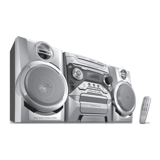
Philips FWD182 Service Manual
Hide thumbs
Also See for FWD182:
- User manual (44 pages) ,
- Specifications (2 pages) ,
- User manual (44 pages)
Table of Contents
Advertisement
Quick Links
Download this manual
See also:
User Manual
Mini System
Service
Service
Service
Service
Service
Service Manual
©
Copyright 2006 Philips Consumer Electronics B.V. Eindhoven, The Netherlands
All rights reserved. No part of this publication may be reproduced, stored in a retrieval system or
transmitted, in any form or by any means, electronic, mechanical, photocopying, or otherwise
without the prior permission of Philips.
Published by SL-ET 0634 Service AudioPrinted in The Netherlands Subject to modification.
Version 1.1
TABLE OF CONTENTS
Location Of Pc Boards ................................................ 1-2
Versions Variation ....................................................... 1-2
Specifications .............................................................. 1-3
Measurement Setup ................................................... 1-4
Service Aids ................................................................ 1-5
ESD & Safety Instruction ............................................ 1-6
Lead-free & Service Information ................................ 1-7
Connection & Preparation ............................. 1-8 to 1-12
Troubleshooting ....................................................... 1-13
Setting Procedure & Repair Instructions ....................... 2
Disassembly Instructions & Service positions .............. 3
Block & Wiring Diagram ................................................ 4
Control Board ................................................................. 5
Main Board .................................................................... 6
Tuner Board ................................................................... 7
Power Board .................................................................. 8
Dvd Loader ................................................................... 9
Mechanical Exploded View & Parts List ...................... 10
Revision List ................................................................ 11
FWD182
Page
VIDEO CD
CLASS 1
GB
/All Versions
3141 785 31021
Advertisement
Table of Contents

Related Manuals for Philips FWD182


Summary of Contents for Philips FWD182
- Page 1 LASER PRODUCT © Copyright 2006 Philips Consumer Electronics B.V. Eindhoven, The Netherlands All rights reserved. No part of this publication may be reproduced, stored in a retrieval system or transmitted, in any form or by any means, electronic, mechanical, photocopying, or otherwise without the prior permission of Philips.
- Page 2 LOCATION OF PC BOARDS TUNER BOARD MAIN BOARD CONTROL BOARD POWER BOARD VERSION VARIATIONS: Type /Versions: FWD182 Features & Board in used: Karaoke Rotary Encoder (volume control) Jog Shuttle Voltage Selector Aux Input Digital Output Headphone Socket Line Output Standby - FTD Clock Display...
-
Page 3: Specifications
AMPLIFIER SECTION Digital Output ..............Output power ........... 1200 W PMPO ....SPDIF (Sony Philips digital interface) Coaxial Stereo mode ........30 W + 30 W RMS PCM ..............IEC 60958 Frequency Response ....150 Hz - 18 kHz / ± 3 dB Dolby Digital/DTS ...... -
Page 4: Measurement Setup
MEASUREMENT SETUP Tuner FM Bandpass LF Voltmeter 250Hz-15kHz e.g. PM2534 e.g. 7122 707 48001 RF Generator e.g. PM5326 S/N and distortion meter e.g. Sound Technology ST1700B Use a bandpass filter to eliminate hum (50Hz, 100Hz) and disturbance from the pilottone (19kHz, 38kHz). Tuner AM (MW,LW) Bandpass LF Voltmeter... - Page 5 SERVICE AIDS ESD Equipment: Service Tools: Universal Torx driver holder .........4822 395 91019 Anti-static table mat - large 1200x650x1.25mm ...4822 466 10953 anti-static table mat - small 600x650x1.25mm ..4822 466 10958 Torx bit T10 150mm ...........4822 395 50456 Anti-static wristband ..........4822 395 10223 Torx driver set T6-T20 .........4822 395 50145 Connectorbox (1M Ω)
-
Page 6: Laser Product
WAARSCHUWING WARNING Alle IC’s en vele andere halfgeleiders zijn All ICs and many other semi-conductors are gevoelig voor electrostatische ontladingen susceptible to electrostatic discharges (ESD). (ESD). Careless handling during repair can reduce life Onzorgvuldig behandelen tijdens reparatie kan drastically. de levensduur drastisch doen verminderen. When repairing, make sure that you are Zorg ervoor dat u tijdens reparatie via een connected with the same potential as the mass... - Page 7 To avoid wear-out of tips switch off un-used equipment, or reduce heat. • Mix of lead-free solder alloy / parts with leaded solder alloy / parts is possible but PHILIPS recommends strongly to avoid mixed solder alloy types (leaded and lead-free).
- Page 10 1-10...
- Page 11 1-11...
- Page 12 1-12...
- Page 13 1-13...
- Page 16 DISMANTLING INSTRUCTIONS Dismantling the DVD Module Dismantling of the Cover Front Display 1) Remove the Volume knobs & Mic knob as stated in Dismantling the Cover Front Display in Figure 7 & 8. 1) Loosen the 4 screws at top cover , 2 screws at slide Cover and 4 screws at back panel as Figure 1 &...
- Page 17 Dismantling of the Key Board and Cassette module Dismantling of the Power Board 1) Loosen 4 screws 'J' to remove the Power Board figure 14. 1) Loosen 13 screws 'H' to remove the KEY board figure 12. Figure 14 Figure 12 2) Remove the catch 'K' using cutter as shown in figure 15.
-
Page 18: Service Positions
Service positions Service position A Service position B Note: After re-assembly, it is very important to ensure the wires are properly inserted into their respective sockets and routed not to touch or obstruct any moving parts. Service position C... - Page 19 SET BLOCK DIAGRAM Main PCB AUX- IN Logic HEX Inverter IC TEA5762H TUNER PACK IC SN7404 COAXIAL OUT IC TC4052B P IC SAA6588T SWITCH Tuner PCB Y.U.V OUT (OR SCART) ES8380 A/D IC CS5340 DVD LOADER u_CO M S-VIDEO SANYO DVD LODER C-VIDEO PLAY/REC 1 TAPE IC IRC4558...
- Page 20 WIRING DIRGRAM Control PCB LVC105880-0001...
- Page 21 FTD DISPLAY PIN ASSIGNMENT KEY & KARAOKE BOARD TABLE OF CONTENTS FTD Display Pin Assignment ........... 5-1 Pin Connection ..............5-1 Circuit Diagram (Key PCB) ..........5-2 Circuit Diagram (Karaoke PCB) ........5-3 PCB Layout Top View ............5-4 PCB Layout Bottom View ..........5-5 Electrical Parts List &...
- Page 22 CIRCUIT DIAGRAM: KEY PCB C2511 C2523 C2535 D2501 IC251 R2506 R2519 R2532 R2544 TA2505 XL2501 C2512 C2524 C2536 D2503 JK5001 R2507 R2520 R2533 R2545 RB201 TA2506 ZD251 C2501 C2513 C2525 C2538 D2504 LD2501 R2508 R2521 R2534 R2546 TA2507 ZD252 C2502 C2514 C2526 C2539...
- Page 23 CIRCUIT DIAGRAM : KARAOKE PCB C3036 C3046 IC3002 Q3007 R3015 R3032 R3043 R3055 R3071 C3037 C3047 IC3003 R2556 R3016 R3033 R3045 R3056 R3072 C3038 C3049 JK3001 R3001 R3023 R3034 R3046 R3059 C3040 C3051 L3001 R3009 R3025 R3035 R3047 R3064 C3042 C3056 PT2396 A1 R3010...
- Page 24 PCB LAYOUT - KEY & KARAOKE (TOP VIEW) C2503 A2 C3044 B1 J11 A2 J22 B5 J34 C2 J45 A4 J8 C2 R2514 A4 R2546 A5 TA2505 B4 TP1 C2504 A5 C3045 B1 J12 A2 J23 B4 J35 C2 J46 A4 J9 C2 R2515 A3 R2550...
- Page 25 PCB LAYOUT - KEY & KARAOKE (BOTTOM VIEW) C2518 C2535 C3035 C5504 IC3003 R2509 R2540 R3013 R3038 R3065 C2519 C2536 C3036 C5505 L3001 R2524 R2541 R3015 R3039 R3066 C2501 C2520 C2538 C3038 C5506 Q2501 R2525 R2543 R3016 R3040 R3067 C2502 C2521 C2539 C3043...
- Page 26 ELECTRICAL PARTS LIST - KEY & KARAOKE BOARD D2506 4822 130 83338 LL4148 D2507 4822 130 83338 LL4148 D2508 4822 130 83338 LL4148 D2509 4822 130 83338 LL4148 D3001 4822 130 83338 LL4148 D3002 4822 130 83338 LL4148 D3003 4822 130 83338 LL4148 DP251 9940 000 05263...
- Page 27 ES8380 PHOENIX INTERNAL IC DIAGRAM Motor DVD/CD Motor Driver MAIN BOARD Video TV Display Audio Speakers SDRAM Audio Microphone In ES8380 (8/16-MB) Phoenix S/P DIF A/V Receiver EEPROM VFD Panel VFD Driver ROM/Flash IR Remote TABLE OF CONTENTS AN7312 INTERNAL IC DIAGRAM INTERNAL IC DIAGRAM .............
- Page 28 CIRCUIT DIAGRAM MAIN SERVO (TOP LEFT) C0201 C0216 C0232 C2003 C206 C223 C238 C253 C269 C285 C322 C803 D802 FB214 C0202 C0217 C0233 C2004 C207 C224 C239 C254 C270 C286 C324 C804 D803 FB215 C0203 C0218 C0234 C2006 C208 C225 C240 C255 C271...
- Page 29 CIRCUIT DIAGRAM MAIN SERVO (TOP RIGHT) FB229 IC209 L210 Q805 R208 R226 R243 R260 R278 R329 R809 R827 RA204 ZD211 FB301 IC210 L211 Q806 R209 R227 R244 R261 R279 R330 R810 R828 RA205 ZD212 FB302 IC303 L212 R201 R210 R228 R245 R262 R281...
- Page 30 CIRCUIT DIAGRAM MAIN SERVO (BOTTOM LEFT) IC _AM5888 C805 470U 470U/10V /10V VP VP A DR FN FN DRFP DRFP C201 C202 C247 680P 680P CL CL OS ESS136P CN 201 FB201 FB201 CL OSES W ESS135P 10 10 EN EN 1 OPENSW ESS137P EN EN 2...
- Page 31 CIRCUIT DIAGRAM MAIN SERVO (BOTTOM RIGHT) OPTI CA L IN EA UX0 UX0 2 LA 5 LO E# CO AX AX IAL- IAL- OU EA UX0 UX0 3 LA 4 R 281 LA 1 GN D LA 1 LA 3 LC S3 LO E# LO E#...
- Page 32 100K OPEN OPEN R450 56 56 +12V Q409 JK JK401C 401C C521 R526 C456 KTC3875 3875 In Dashed part FWD182 OPEN FWD186 USE Only DI DIN_ N_MU MUTE 47U/16V /16V 220K 220K REC_ REC_L R313 R314 REC_ REC_R R548 R546...
- Page 33 CIRCUIT DIAGRAM MAIN AMPLIFIER (BOTTOM) Q506 R303 R320 R417 R436 R5006 R509 R524 R540 R709 R727 R744 ZD302 Q507 R304 R351 R418 R437 R5007 R510 R525 R541 R710 R728 R746 ZD501 Q701 R305 R352 R420 R439 R5008 R511 R526 R542 R711 R729 R747...
- Page 34 PCB LAYOUT: MAIN (TOP) VIEW C0224 A3 C318 C711 A1 D519 L212 R271 C4 R443 R726 B2 ZD702 B1 C0232 B5 C320 C712 A2 D520 L214 R273 C4 R444 R727 C2 ZD901 D2 C0239 D6 C321 C713 B2 D701 L215 R274 C4 R450 R729...
- Page 35 PCB LAYOUT MAIN (BOTTOM) VIEW C0201 C263 FB228 C0202 C270 FB229 C0203 C271 Q201 C0204 C272 Q410 C0205 C298 Q411 C0206 C319 R2019 C0207 C327 R2022 C0208 C328 R210 C0209 C329 R212 C0210 C333 R214 C0211 C334 R216 C0212 C347 R217 C0213 C348...
- Page 36 6-10 6-10 VOLTAGE IC201 ES8380FAA IC207 74HCU04D Pin NO Pin NO Voltage Voltage Pin NO Voltage IC209 N74F138D Pin NO Pin NO Voltage Voltage Pin NO Voltage IC210 74F244 Pin NO Pin NO Voltage Voltage Pin NO Voltage IC301 CO4558A Pin NO Pin NO Voltage...
- Page 37 6-11 6-11 ELECTRICAL PARTS LIST - MAIN BOARD ELECTRICAL PARTS LIST - MAIN BOARD D201 9940 000 05203 DIODE UF4007 JK203 9940 000 00857 RCA JACK 3P R-B-G XL201 9940 000 05201 X'TAL 27MHZ H3.5MM D202 9940 000 05203 DIODE UF4007 JK401 9940 000 00859 RCA JACK 4P AUDIO IN...
- Page 38 TUNER ADJUSTMENT TABLE Waverange Input frequency Input Tuned to Adjust Output Scope/Voltmeter VARICAP ALIGNMENT 108MHz 7.5V 1V check 87.5 - 108MHz (50kHz grid) 87.5MHz check 1.4V 0.2V 1602KHz check 7.2V 1V T005 531KHz 1.1V 0.2V 531-1602kHz (9kHz grid) TUNER BOARD 530-1700kHz 1700KHz check...
- Page 39 CIRCUIT DIAGRAM : TUNER BOARD (/ 51 ver.) ANT001 A1 C020 C030 C039 C047 D001 IF002 R002 R010 R018 R028 T001 VD002 C002 C011 C021 C031 C040 C048 D002 IF003 R003 R011 R019 R029 T002 VR001 C004 C012 C022 C032 C041 C049 D003...
- Page 40 CIRCUIT DIAGRAM : TUNER BOARD (/55 & /98 ver.) ANT001 C011 C022 C033 C043 D004 Q003 R016 R027 VC001 C002 C012 C023 C034 C044 D005 Q004 R017 R028 VC002 C004 C013 C024 C035 C047 IC001 R001 R018 R029 VD001 C005 C014 C025 C036...
- Page 41 PCB LAYOUT - TUNER BOARD (TOP VIEW) - / 51ver. ANT001 A2 CN002 C004 D001 C005 D002 C008 D003 C009 D004 C010 D005 C017 EF450-G1 C019 IC001 IF001 C025 IF002 C029 IF003 L004 C030 Q002 C036 Q003 C037 R005 C038 T001 C039 T002...
- Page 42 PCB LAYOUT - TUNER BOARD (TOP VIEW) - /55 & /98ver. ANT001 A2 JMP4 C005 JMP5 C006 JMP6 C007 JMP7 C009 JMP8 JMP9 C019 L001 C024 C025 Q001 C030 Q002 C035 R018 C047 T001 CN001 T002 CN002 T003 D001 T005 D002 T006 D003...
- Page 43 VOLTAGE Pin NO Vlotage Pin NO Voltage POWER BOARD Pin NO Voltage Pin NO Voltage Pin NO Pin NO Voltage Voltage Pin NO Pin NO TABLE OF CONTENTS Voltage Voltage Voltage ................8-1 Circuit Diagram ..............8-2 PCB Layout ..............8-3 Pin NO Pin NO Electrical Parts List ............
- Page 44 CIRCUIT DIAGRAM-POWER BOARD BD901 CN903 R917 C901 CN904 R918 C902 D901 R919 C903 D902 R920 C904 D903 R921 C905 D904 R922 C906 D905 R923 C907 D906 R924 C908 D907 R925 C909 D908 R926 C910 D909 R927 C911 D910 R928 C913 D911 R929 C914...
- Page 45 PCB LAYOUT-POWER BOARD BD901 C913 C928 C940 C955 D904 IC901 J910 L907 Q906 R908 R920 R932 R945 R982 C901 C914 C929 C942 C956 D905 IC902 J911 NTC901 Q907 R909 R921 R933 R951 R983 C902 C916 C930 C943 C970 D906 IC903 J912 R946 Q908...
- Page 46 ELECTRICAL PARTS LIST - POWER BOARD BD901 9940 000 02065 RECTIFIER GBU4J 4A 600V L904 9965 000 16694 6µH 13.5TS 2UEW C901 9965 000 27115 CAP. SAFTY 102PF 250V 20% L905 9965 000 16694 6µH 13.5TS 2UEW C902 9940 000 05238 CAP.
- Page 47 DVD LOADER It is not recommended for component repair on this Module but to replace the whole assembly when it becomes defective. Therefore limited service parts list is only for reference. TABLE OF CONTENTS Explorer View (DVD Loader)...........9-2 Mechanical Part list ............9-3...
- Page 48 Explorer View - DVD Loader...
- Page 49 MECHANICAL PART LIST - DVD LOADER LOADER BASE LOADER TRAY FRONT DAMPER RAR DAMPER TRAY MOTOR CLAMPER TOP CLAMPER DOWN GEAR PULLEY LIMIT SWITCH CONNECTOR SCREW FOR GEAR PULLEY SCREW FOR PCB SCREW FOR FRONT DAMPER SCREW FOR REAR DAMPER SCREW FOR TRAY MOTOR...
- Page 50 10-1 10-1 SET MECHANICAL EXPLODED VIEW...
- Page 51 10-2 10-2 MECHANICAL & ACCESSORIES PARTS LIST 9940 000 05296 CASSETTE DOOR LENS 9940 000 01054 LINE CORD 2P 2000MM 9940 000 05275 CASSETTE DOOR 9940 000 02731 FM ANTENNA 1500MM 9940 000 05307 CASS DOOR SPRING 9940 000 05267 AM LOOP ANT 1300 5TS 2P 9940 000 05282 MIC KNOB...
- Page 52 11-1 REVISION LIST 1.0 Manual 3141 785 31020 Initial Service Manual released. 1.1 Manual 3141 785 31021 In this version, the version /68 and version /79 are added. P6-11 : Electrical Parts List - Main Board updated P10-2 : Mechanical Partslist updated...
Need help?
Do you have a question about the FWD182 and is the answer not in the manual?
Questions and answers