Sony MZ-R910 Service Manual
Portable minidisc recorder
Hide thumbs
Also See for MZ-R910:
- Operating instructions manual (37 pages) ,
- Operating instructions manual (120 pages)
Table of Contents
Advertisement
Quick Links
SERVICE MANUAL
Ver 1.0 2002. 06
US and foreign patents licensed from Dolby
Laboratories.
Audio playing system
MiniDisc digital audio system
Laser diode properties
Material:GaAlAs
Wevelength : λ =790nm
Emissin duration : continuous
Laser output : less than 44.6 µW
(This output is the value measured at a distance of 200 mm from the
lens surface on the optial pick-up block with 7 mm aperture.)
Recording and playback time (when using MDW-80)
Maximum 160 min. in monaural
Maximum 320 min. in stereo
Revolutions
382 rpm to 2,700 rpm (CLV)
Error correction
ACIRC (Advanced Cross Interleave Reed Solomon Code)
Sampling frequency
44.1 kHz
Sampling rate converter
Input : 32 kHz/44.1 kHz/48 kHz
Coding
ATRAC (Adaptive TRansform Acoustic Coding)
ATRAC3 - LP2/LP4
Modulation system
EFM (Eight to Fourteer Modulation)
Frequency response
20 to 20,000 Hz ± 3 dB
Wow and Flutter
Below measurable limit
Sony Corporation
9-874-055-01
2002F0200-1
Personal Audio Company
C 2002.06
Published by Sony Engineering Corporation
Model Name Using Similar Mechanism
Mechanism Type
Optical Pick-up Name
SPECIFICATIONS
Inputs
1)
MIC : sterto mini-jack
(minimum input level 0.25 mV)
Line in :
stereo mini-jack for anolog input (minimum input level 49 mV)
optical (digital) mini-jack for optical (digital) input
Outputs
i/LINE OUT
194 mv(10 kohm)
Maximum output(DC)
Headphones : 5 mW + 5 mW(16 ohm)
Power requirements
Sony AC Power Adaptor connected at the DC IN 3V jack (country
model in parentheses) :
230 - 240 V AC, 50 Hz (Hong Kong)
100 - 240 V AC, 50/60 Hz (Tourist)
The recorder :
Nickel metal hydride rechargeable battery
NH-14WM(A) 1.2V 1350 mAh (MIN) Ni-MH
LR6 (SG) alkaline battery
Battery charging stand:
AC power adaptor DC 3V
Dimensions
Approx.78.9 x 72.0 x17.1 mm (w/h/d)
(3
1
/
x 2
7
/
8
8
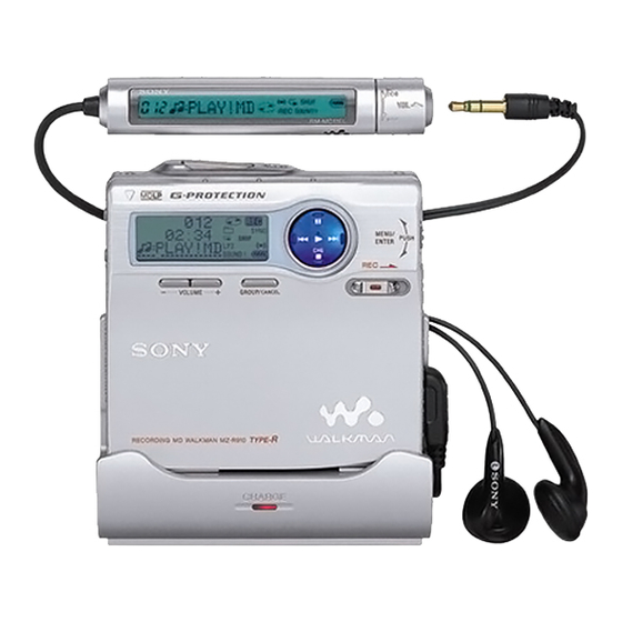
PORTABLE MINIDISC RECORDER
MZ-R910
Hong Kong Model
Tourist Model
2)
: stereo mini-jack (dedicated remote control jack) /
2)
x
11
/
in.)
16
– Continued on next page –
NEW
MT-MZR910-180
LCX-5RV
Advertisement
Table of Contents

Related Manuals for Sony MZ-R910


Summary of Contents for Sony MZ-R910
- Page 1 Headphones : 5 mW + 5 mW(16 ohm) Power requirements Maximum 320 min. in stereo Revolutions Sony AC Power Adaptor connected at the DC IN 3V jack (country 382 rpm to 2,700 rpm (CLV) model in parentheses) : Error correction...
- Page 2 Whe n us ing a 100% fully charged metal hydride rechargeable battery (NH- 14WM(A)). When using a Sony LR6 (S G) “STAMINA ” a lka line dry battery (produced in Japan) SAFETY-RELATED COMPONENT WARNING!! COMPONENTS IDENTIFIED BY MARK 0 OR DOTTED...
-
Page 3: Table Of Contents
MZ-R910 TABLE OF CONTENTS SERVICING NOTES ..........4 GENERAL ..............5 DISASSEMBLY 3-1. Disassembly Flow ............6 3-2. Panel Assy, Bottom ............6 3-3. Panel Assy, Upper Section ..........7 3-4. “LCD Module”, “Panel Assy,Upper” ......7 3-5. MAIN Board Assy ............8 3-6. -
Page 4: Servicing Notes
MZ-R910 SECTION 1 SERVICING NOTES • The shipment data will be cleared when the NV is reset. There- NOTES ON HANDLING THE OPTICAL PICK-UP fore, change the NV adjusted values following the Change of BLOCK OR BASE UNIT NV Adjusted Values immediately after the NV was reset. (See... -
Page 5: General
MZ-R910 SECTION 2 This section is extracted from instruction manual. GENERAL Looking at controls The display window of the recorder The recorder 1 Character information display 6 Play mode intication Displays the disc and track names, Shows the play mode (shuffle play, date, error messages, track numbers, program play, repeat play, etc.) of... -
Page 6: Disassembly
MZ-R910 SECTION 3 DISASSEMBLY Note: Disassemble the unit in the order as shown below. 3-1. DISASSEMBLY FLOW 3-2. Panel Assy, 3-3. Panel Assy, 3-5. Main Board Assy 3-6. “Case Assy, Battery”, Bottom Upper Section “Main Board” 3-4. “LCD Module”, “Panel Assy, Upper”... -
Page 7: Panel Assy, Upper Section
MZ-R910 3-3. PANEL ASSY, UPPER SECTION 3 Two ES lock screws 1 Flexible board (CN801) 4 Panel assy, upper 3 Two ES lock screws 2 Push the button (open). 3-4. “LCD MODULE”, “PANEL ASSY, UPPER” 1 Three screws (1.7) 2 Remove the LCD module in the direction of the arrow. -
Page 8: Main Board Assy
MZ-R910 3-5. MAIN BOARD ASSY 6 Flexible board (CN501) 7 Main board assy 1 Remove two solders of flexible board. 3 Four screws (M1.4 toothed lock) 2 Flexible board 4 ES lock screw (CN502) 3-6. “CASE ASSY, BATTERY”, “MAIN BOARD”... -
Page 9: Strip, Ornamental
MZ-R910 1 Pull toward the direction A 3-7. STRIP, ORNAMENTAL to disengage two bosses 5 Remove the “strip, ornamental” in the direction of arrow C . Note: As the “strip, ornamental” is very fragile, do not give an excessive force to the entire assy when removing it. -
Page 10: Service Assy, Op (Lcx-5Rv)
MZ-R910 3-9. SERVICE ASSY, OP (LCX-5RV) 2 Gear (SA) 5 Screw (M1.4) 1 Washer (0.8-2.5) 6 Spring, thrust detent 3 Screw (M1.4) 8 Pull off “screw, lead” 4 Spring, rack 9 Opening the over write head toward the direction A , remove the “service assy, OP (LCX-5RV) toward the direction B . -
Page 11: Holder Assy
MZ-R910 3-10. HOLDER ASSY 5 Remove the holder assy in the direction of arrow D . 2 Push the convex portion toward the direction B and 1 Open the holder assy. open the holder assy toward the direction A to erect uprightly. -
Page 12: Motor, Dc (Spindle) (M601)", "Motor, Dc (Over Write Head Up/Down) (M603)
MZ-R910 3-12. “MOTOR, DC (SPINDLE) (M601)”, “MOTOR, DC (OVER WRITE HEAD UP/DOWN) (M603)” 1 Remove six solders of motor flexible board. Note: Press-fit the gear (HA) up to the position of the “motor, DC (over qa Motor, DC (over write head up/down) -
Page 13: Test Mode
MZ-R910 SECTION 4 TEST MODE Outline Operation in Setting the Test Mode • This set provides the Overall adjustment mode that allows CD • When the test mode becomes active, first the display check mode and MO discs to be automatically adjusted when in the test mode. - Page 14 MZ-R910 Configuration of Test Mode [VOLUME +] key: 100th place of item [Major item switching] number increase. [Test Mode $Display Check Mode%] [VOLUME --] key: 100th place of item [VOLUME +] Press the > number decrease. x/CHG [Manual Mode] Press the...
- Page 15 MZ-R910 5. The display changes a shown below each time the jog Self-Diagnosis Result Display Mode [DISPLAY] dial (down) is turned or the key on the remote This set uses the self-diagnostic function system in which if an commander is pressed.
- Page 16 MZ-R910 • Description of error indication codes Problem Indication code Meaning of code Simple display Description No error No error No error Illegal access target Adrs Attempt to access an abnormal address address was specified Servo system error High temperature...
- Page 17 MZ-R910 Sound Skip Check Result Display Mode Jog and Key Check Mode This set can display the count of errors that occurred during the This set can check if the set and remote commander function nor- recording/playing for checking. mally.
- Page 18 MZ-R910 Example1: When the key on the set is pressed: > Remote commander LCD display ** : AD value of the remote commander key (hexadecimal 00 to FF) Example2: When the key on the remote commander N > is pressed:...
-
Page 19: Electrical Adjustments
2. Use the following tools and measuring instruments. • Test CD disc TDYS-1 2. Press the X key. (Part No. : 4-963-646-01) Remote commander LCD display • SONY MO disc available on the market • Digital voltmeter ResOK? • Laser power meter LPM-8001 (Part No. : J-2501-046-A) 3. - Page 20 MZ-R910 [VOLUME +] [VOL- [VOLUME +] [VOL- 2) Adjust with the key (adjusted value up) or 20) Adjust with the key (adjusted value up) or UME --] UME --] key (adjusted value down) so that the adjusted value key (adjusted value down) so that the adjusted value becomes 08.
- Page 21 MZ-R910 1. Connect a digital voltmeter to the AP914 (VC) on the MAIN 1. Connect a digital voltmeter to the AP915 (VL) on the MAIN [VOLUME +] [VOLUME --] [VOLUME +] [VOLUME board, and adjust key (voltage up) or board, and adjust key (voltage up) or + 0.005...
- Page 22 MZ-R910 1. Connect a digital voltmeter to the AP911 (VD) on the MAIN 4. Press the N key, and set the laser MO read adjustment mode [VOLUME +] [VOLUME board, and adjust key (voltage up) or (item number 011). key (voltage down) so that the voltage becomes 1.31 ± 0.010...
- Page 23 MZ-R910 Adjustment/checking and Connection Location: – MAIN Board (Conductor Side) – TP (+) TP (–) AP911 (VD) AP915 (VL) AP914 (VC) C212 IC303 IC551 R503 C510 IC301 C502 C511 C527 C513 IC501 C519 C303 C218 C532 C505 C301 C514 R218...
- Page 24 MZ-R910 Overall Adjustment Mode • Overall adjustment mode (title display) • Configuration of overall adjustment mode Remote commander LCD display Assy** Overall adjustment mode (Title display) : (Disc mark) At end of power supply adjustment: Outside lit At end of electrical offset adj.: Inside lit Protect switch Note: On the set having microcomputer version 1.000, the disc...
- Page 25 MZ-R910 5. If OK through the CD overall adjustments, then perform MO 2. MO overall adjustment items overall adjustments. Item No. Description Remote commander LCD display CD OK MO electrical offset adjustment 6. Insert MO disc in the set, and press the > key to set the MO overall adjustment mode.
- Page 26 MZ-R910 [VOLUME +] Patch Data Rewriting When Nonvolatile Memory 12. Press the key three times to change the blink- ing portion to 115C. was Replaced On this set, if the nonvolatile memory was replaced, the modified Remote commander LCD display program data must be written to the nonvolatile memory.
- Page 27 MZ-R910 [VOLUME +] [VOLUME +] 24 Press the key once to change the blinking por- 38. Adjust with the key (adjusted value up) or [VOLUME --] tion to 1179. key (adjusted value down) so that the adjusted value becomes 7C.
- Page 28 MZ-R910 [VOLUME +] 66. Adjust with the key (adjusted value up) or 51. Press the X key. [VOLUME --] key (adjusted value down) so that the adjusted (117F is blinking) value becomes 03. [VOLUME +] 52. Press the key twice to change the blinking por- tion to 1181.
- Page 29 MZ-R910 [VOLUME +] [VOLUME +] 80. Press the key once to change the blinking por- 94. Adjust with the key (adjusted value up) or [VOLUME --] tion to 1188. key (adjusted value down) so that the adjusted value becomes E0.
- Page 30 MZ-R910 [VOLUME +] [VOLUME +] 108. Press the key once to change the blinking por- 122. Adjust with the key (adjusted value up) or [VOLUME --] tion to 1192. key (adjusted value down) so that the adjusted value becomes A0.
- Page 31 MZ-R910 [VOLUME +] [VOLUME +] 136. Press the key once to change the blinking por- 150. Adjust with the key (adjusted value up) or [VOLUME --] tion to 1199. key (adjusted value down) so that the adjusted value becomes 80.
- Page 32 MZ-R910 [VOLUME +] [VOLUME +] 164. Press the key three times to change the blink- 178. Adjust with the key (adjusted value up) or [VOLUME --] ing portion to 11A3. key (adjusted value down) so that the adjusted value becomes E5.
- Page 33 MZ-R910 [VOLUME +] [VOLUME +] 192. Press the key once to change the blinking por- 206. Adjust with the key (adjusted value up) or [VOLUME --] tion to 11AB. key (adjusted value down) so that the adjusted value becomes 18.
- Page 34 MZ-R910 [VOLUME +] [VOLUME +] 220. Press the key twice to change the blinking por- 234. Adjust with the key (adjusted value up) or [VOLUME --] tion to 11B5. key (adjusted value down) so that the adjusted value becomes 02.
- Page 35 MZ-R910 [VOLUME +] [VOLUME +] 248. Press the key once to change the blinking por- 262. Adjust with the key (adjusted value up) or [VOLUME --] tion to 11BC. key (adjusted value down) so that the adjusted value becomes E1.
- Page 36 MZ-R910 [VOLUME +] [VOLUME +] 276. Press the key once to change the blinking por- 290. Adjust with the key (adjusted value up) or [VOLUME --] tion to 11C4. key (adjusted value down) so that the adjusted value becomes 85.
- Page 37 MZ-R910 [VOLUME +] [VOLUME +] 304. Press the key twice to change the blinking por- 318. Adjust with the key (adjusted value up) or [VOLUME --] tion to 11CE. key (adjusted value down) so that the adjusted value becomes DA.
- Page 38 MZ-R910 [VOLUME +] [VOLUME +] 332. Press the key once to change the blinking por- 346. Adjust with the key (adjusted value up) or [VOLUME --] tion to 11D8. key (adjusted value down) so that the adjusted value becomes E3.
- Page 39 MZ-R910 [VOLUME +] [VOLUME +] 360. Press the key once to change the blinking por- 374. Adjust with the key (adjusted value up) or [VOLUME --] tion to 11DF. key (adjusted value down) so that the adjusted value becomes B0.
- Page 40 MZ-R910 [VOLUME +] [VOLUME +] 388. Press the key once to change the blinking por- 402. Adjust with the key (adjusted value up) or [VOLUME --] tion to 11E6. key (adjusted value down) so that the adjusted value becomes C4.
- Page 41 MZ-R910 [VOLUME +] [VOLUME +] 416. Press the key once to change the blinking por- 430. Adjust with the key (adjusted value up) or [VOLUME --] tion to 11EF. key (adjusted value down) so that the adjusted value becomes CB.
- Page 42 MZ-R910 [VOLUME +] [VOLUME +] 444. Press the key once to change the blinking por- 458. Adjust with the key (adjusted value up) or [VOLUME --] tion to 11F7. key (adjusted value down) so that the adjusted value becomes 8E.
- Page 43 MZ-R910 [VOLUME +] [VOLUME +] 472. Press the key once to change the blinking por- 486. Adjust with the key (adjusted value up) or [VOLUME --] tion to 11FE. key (adjusted value down) so that the adjusted value becomes 01.
-
Page 44: Diagrams
MZ-R910 SECTION 6 DIAGRAMS 6-1. NOTE FOR PRINTED WIRING BOARD AND SCHEMATIC DIAGRAMS Note on Printed Wiring Board: Note on Schematic Diagram: • X : parts extracted from the component side. • All capacitors are in µF unless otherwise noted. pF: µµF •... - Page 45 MZ-R910 • Waveforms IC902 5 (EXT) IC301 qs (LRCK) IC501 1 (TE) IC801 (TE) (REC mode) 3.7 Vp-p 2 Vp-p 840 mVp-p 840 mVp-p 22.7 µ s 2.6 µ s IC301 qa (MCLK) IC501 8, 9, 0, qa IC901 th (CLK)
-
Page 46: Block Diagram - Servo Section
MZ-R910 6-2. BLOCK DIAGRAM – SERVO Section – OVER WRITE HEAD DRIVE IC601 (1/2) HR601 OVER WRITE OVER HEAD DRIVE OPTICAL PICK-UP BLOCK WRITE PRE DRIVER Q604, 605 (LCX-5RV) HEAD (Page 48) VRECIN2 OUTA VRECO M603 H-BRIDGE OUTB VRECIN1 RF AMP, FOCUS/TRACKING ERROR AMP... -
Page 47: Block Diagram - Audio Section
MZ-R910 6-3. BLOCK DIAGRAM – AUDIO Section – OPTICAL RECEIVER B+ SWITCH VIF B+ Q302 DIN1 (Page 46) J301 LINE IN (OPT) (LINE IN JACK) A/D CONVERTER IC301 MIC AMP IC303 J303 LIN2 OUT2 LIN1 (PLUG IN POWER) AUDIO ADDT... -
Page 48: Block Diagram - Display/Key Control/Power Supply Section
MZ-R910 6-4. BLOCK DIAGRAM – DISPLAY/KEY CONTROL/POWER SUPPLY Section – RMC KEY (Page 47) VRMC HEADPHONE AMP (IC302), XWK3 MOTOR/COIL DRIVER (IC551) RMC KEY CLK SEL CLK SEL FFCLR FFCLR SLEEP SLEEP SYSTEM VLON (Page 46) CONTROL VLON XWK1 POWER CONTROL... -
Page 49: Main Board (Component Side)
MZ-R910 6-5. PRINTED WIRING BOARD – MAIN Board (Component Side) – :Uses unleaded solder. • Semiconductor Location Ref. No. Location Q602 S802 Q902 PROTECT DETECT S806 OPEN MAIN BOARD (COMPONENT SIDE) S803 RECHARGEABLE J301(1/2) S801 BATTERY IN LINE IN DETECT... -
Page 50: Printed Wiring Board - Main Board (Conductor Side)
MZ-R910 6-6. PRINTED WIRING BOARD – MAIN Board (Conductor Side) – :Uses unleaded solder. • Semiconductor MAIN BOARD (CONDUCTOR SIDE) Location Ref. No. Location D301 M602 D303 (SLED) D601 D602 FLEXIBLE BOARD D603 M603 D606 OVER WRITE HEAD UP/DOWN D607... -
Page 51: Schematic Diagram – Main Board (1/4)
MZ-R910 6-7. SCHEMATIC DIAGRAM – MAIN Board (1/4) – • See page 60 for IC Pin Function Description. -
Page 52: Schematic Diagram - Main Board (1/4)
MZ-R910 6-8. SCHEMATIC DIAGRAM – MAIN Board (2/4) –... -
Page 53: Schematic Diagram - Main Board (3/4)
MZ-R910 6-9. SCHEMATIC DIAGRAM – MAIN Board (3/4) – • See page 61 for IC Pin Function Description. -
Page 54: Schematic Diagram - Main Board (4/4)
MZ-R910 6-10. SCHEMATIC DIAGRAM – MAIN Board (4/4) –... -
Page 55: Ic Block Diagrams
MZ-R910 • IC Block Diagrams IC301 AK5354VT-E2 16 PDN LIN1 15 CSN CONTROL IPGA 14 CCLK RIN1 REGISTER LIN2 13 CDTI RIN2 CLOCK DIVIDER VCOM 12 LRCK AGND 11 MCLK AUDIO I/F CONTROLLER 10 BCLK 9 SDTO IC302 AN17020A-VB HEADPHONE... - Page 56 MZ-R910 IC501 SN761057ADBT ADIP-IN S-MON A+B+C+D TWpp PK/BTM CSLO REXT VREF075 Aw+Dw Wpp LPF S-MONITOR TON Peak VREF TON Botm Malfa ADIP AwBPF TEMP DwBPF Tpp/Wpp ABCD OFC-C1 OFC-C2 AVCC AGND CCSL2 ABCD VREF075 PEAK PEAK/BOTM BOTM TON-C OF TRK...
- Page 57 MZ-R910 IC551 SC111258FCR2 42 41 35 34 31 30 29 PWM2 3PHASE CONTROL 3PHASE H-BRIDGE H-BRIDGE PRE DRIVER PRE DRIVER CONTROL VC LOW VOLTAGE DETECTOR COM2 CPUI2 – CPUO2 CPVO2 – CPVI2 CPWO2 CPWI2 – BIAS GND2 VC VG GND1 –...
- Page 58 MZ-R910 IC601 XPC18A22AFCR2 VC2 VG CHARGE OUTPUT SW OUTPUT SW CHARGE PUMP 1 PUMP 2 VC VG DC IN HI-BRIDGE CHARGE PRE DRIVER PRE DRIVER MONITOR VREF VREF X2/X4 BATM BUFFER DC IN CVREF CONTROL CONTROL CHARGE CHGSW DW BT...
- Page 59 MZ-R910 IC901 XPC18A32AFCR2 36 35 34 33 32 31 30 29 OUTPUT OUTPUT SW SERIES PASS SERIES PASS SERIES PASS OUTPUT SW REGULATOR VA REGULATOR VD REGULATOR VIF POWER – SWITCH 1 INM1 STEP-UP PRE DRIVER DTC1 XRST OUTPUT SW...
-
Page 60: Ic Pin Function Description
MZ-R910 6-11. IC PIN FUNCTION DESCRIPTION • IC501 SN761057ADBT (RF AMP, FOCUS/TRACKING ERROR AMP) Pin No. Pin Name Description Tracking error signal output to the system controller REXT — Connect terminal to the external resistor for the ADIP amplifier control WPP-LPF —... - Page 61 MZ-R910 • IC801 CXD2677-204GA (SYSTEM CONTROLLER, DIGITAL SIGNAL PROCESSOR, 16M BIT D-RAM) Pin No. Pin Name Description Load address strobe signal output terminal for D-RAM Not used Test input terminal for D-RAM Not used 3 to 7 Address signal output terminal for D-RAM Not used...
- Page 62 MZ-R910 Pin No. Description Pin Name Data input terminal Not used TRST Setting terminal for the test mode (normally fixed at “L”) XOPT CTL Power supply ON/OFF control signal output for the DIN PD drive VG CTL VG power supply voltage control signal output terminal Not used...
- Page 63 MZ-R910 Pin No. Description Pin Name XUDP UP ON Pull-up resistor changeover control signal output of USB data (+) output terminal Not used LCD RST Reset control signal output to the liquid crystal display element module L : reset XMUTE...
- Page 64 MZ-R910 Pin No. Description Pin Name — VDIOSC Power supply terminal (for the OSC cell) (+2.2V) OSCI System clock (45.1584MHz) input terminal OSCO System clock (45.1584MHz) output terminal VSIOSC Ground terminal (for the OSC cell) — DAVDD Power supply terminal (for the built-in D/A converter) (+2.2V)
- Page 65 MZ-R910 Pin No. Description Pin Name ADDT Data input from the external A/D converter LRCK L/R sampling clock signal (44.1KHz) output to the external A/D converter XBCK Bit clock signal (2.8224MHz) output to the external A/D converter FS256 11.2896MHz clock signal output to the external A/D converter Clock signal input from the external VCO Not used —...
- Page 66 MZ-R910 Pin No. Description Pin Name Address signal output terminal for D-RAM Not used Output enable signal output terminal for D-RAM Not used Data write enable signal output terminal for D-RAM Not used TSTDR3 Test input terminal for D-RAM Not used EVA/FLASH chip discrimination terminal “L”: FLASH chip, “H”: EVA chip...
-
Page 67: Exploded Views
MZ-R910 SECTION 7 EXPLODED VIEWS NOTE: • -XX and -X mean standardized parts, so they • Items marked “*” are not stocked since they The components identified by mark ! or are seldom required for routine service. Some may have some difference from the original dotted line with mark ! are critical for safety. -
Page 68: Chassis Section
MZ-R910 7-2. CHASSIS SECTION MT-MZR910-180 Ref. No. Part No. Description Remark Ref. No. Part No. Description Remark 3-220-477-01 SHEET (MD), INSULATING 3-244-690-01 SCREW (M1.4), TOOTHED LOCK X-3379-320-6 CHASSIS ASSY, SET 4-223-110-03 TERMINAL (3) 3-225-996-04 SCREW (M1.4)(EG),PRECISION PAN 3-226-169-01 SPACER (PRO) -
Page 69: Md Mechanism Deck Section (Mt-Mzr910-180)
MZ-R910 7-3. MD MECHANISM DECK SECTION (MT-MZR910-180) M603 not supplied M602 M601 The components identified by mark ! or dotted line with mark ! are critical for safety. Replace only with part number specified. Ref. No. Part No. Description Remark Ref. -
Page 70: Electrical Parts List
MZ-R910 SECTION 8 ELECTRICAL PARTS LIST MAIN NOTE: The components identified by • Due to standardization, replacements in the • Items marked “*” are not stocked since they 0 or dotted line with mark mark parts list may be different from the parts speci- are seldom required for routine service. - Page 71 MZ-R910 MAIN Ref. No. Part No. Description Remark Ref. No. Part No. Description Remark C564 1-119-923-81 CERAMIC CHIP 0.047uF C835 1-107-819-11 CERAMIC CHIP 0.022uF C566 1-125-777-11 CERAMIC CHIP 0.1uF C836 1-125-777-11 CERAMIC CHIP 0.1uF C570 1-164-943-11 CERAMIC CHIP 0.01uF C839 1-164-943-11 CERAMIC CHIP 0.01uF...
- Page 72 MZ-R910 MAIN Ref. No. Part No. Description Remark Ref. No. Part No. Description Remark <FERRITE BEAD> Q905 8-729-037-75 TRANSISTOR UN9214J-(TX).SO Q906 8-729-429-44 TRANSISTOR XP1501 FB301 1-216-864-11 METAL CHIP 1/16W Q907 8-729-055-32 TRANSISTOR 3LN01SS-TL FB303 1-216-809-11 METAL CHIP 1/16W FB304 1-216-809-11 METAL CHIP...
- Page 73 MZ-R910 MAIN Ref. No. Part No. Description Remark Ref. No. Part No. Description Remark R612 1-218-985-11 RES-CHIP 470K 1/16W R928 1-218-989-11 RES-CHIP 1/16W R613 1-218-957-11 RES-CHIP 2.2K 1/16W R929 1-218-989-11 RES-CHIP 1/16W R614 1-218-965-11 RES-CHIP 1/16W R930 1-218-989-11 RES-CHIP 1/16W...
- Page 74 MZ-R910 Ref. No. Part No. Description Remark ACCESSORIES *********** ADAPTOR, ATTACHMENT ASSY 0 501 1-476-855-11 ADAPTOR, AC (AC-ES305) (JEW) 0 501 1-476-858-11 ADAPTOR, AC (AC-ES305) (HK) CHARGE UNIT 1-476-763-31 CHARGE UNIT (ASSEMBLED) 1-476-395-12 REMOTE CONTROL UNIT 8-954-008-90 RECEIVER, EAR MDR-E808SP...
- Page 75 MZ-R910 MEMO...
- Page 76 MZ-R910 REVISION HISTORY Clicking the version allows you to jump to the revised page. Also, clicking the version at the upper right on the revised page allows you to jump to the next revised page. Ver. Date Description of Revision...